Short-range phase coherence and origin of the 1T -TiSe
2charge density wave
B. Hildebrand,1,*T. Jaouen,1,†C. Didiot,1E. Razzoli,1G. Monney,1M.-L. Mottas,1A. Ubaldini,2H. Berger,3C. Barreteau,2 H. Beck,1D. R. Bowler,4and P. Aebi1
1D´epartement de Physique and Fribourg Center for Nanomaterials, Universit´e de Fribourg, CH-1700 Fribourg, Switzerland 2Department of Quantum Matter Physics, University of Geneva, 24 Quai Ernest-Ansermet, 1211 Geneva 4, Switzerland
3Institut de G´enie Atomique, Ecole Polytechnique F´ed´erale de Lausanne, CH-1015 Lausanne, Switzerland 4London Centre for Nanotechnology and Department of Physics and Astronomy, University College London,
London WC1E 6BT, United Kingdom
(Received 11 February 2016; revised manuscript received 8 March 2016; published 28 March 2016) The impact of variable Ti self-doping on the 1T -TiSe2charge density wave (CDW) is studied by scanning
tunneling microscopy. Supported by density functional theory, we show that agglomeration of intercalated-Ti atoms acts as preferential nucleation centers for the CDW that breaks up in phase-shifted CDW domains whose size directly depends on the intercalated-Ti concentration and which are separated by atomically sharp phase boundaries. The close relationship between the diminution of the CDW domain size and the disappearance of the anomalous peak in the temperature-dependent resistivity allows to draw a coherent picture of the 1T -TiSe2
CDW phase transition and its relation to excitons. DOI:10.1103/PhysRevB.93.125140
The understanding of broken-symmetry ground states is facing the complexity of the many-body problem arising from the multiplicity of coupled electron-electron, electron-hole, and electron-lattice interactions. A typical material exhibiting this close entanglement is the quasi-two-dimensional, lay-ered transition-metal dichalcogenide 1T -TiSe2 consisting of
hexagonal 1T -stacked Se-Ti-Se layers separated by a van der Waals (vdW) gap. At TCDW ∼200 K, it undergoes a
phase transition towards a 2× 2 × 2 commensurate charge density wave (CDW) phase at which a weak periodic lattice distortion develops and it shows a broad maximum in the temperature-dependent resistivity in the vicinity of TCDW[1].
1T -TiSe2 is also superconducting upon Cu intercalation [2],
and under pressure [3], thus offering the way for the study of the interplay between ordered CDW phase and the supercon-ducting state [4].
However, the origin of the CDW transition itself is not yet unambiguously determined. Although many propositions have been made since the 1970s, there still remain two competing hypotheses for the mechanism driving the CDW formation. Several studies have highlighted strong electron-phonon [5–7] coupling suggesting a Jahn-Teller (JT) mechanism of the CDW transition [first-order JT [8] or pseudo-JT (PJT) [9]]. Electron-hole correlations leading to the excitonic insulator [10,11] or inducing fluctuations responsible for phonon softening [12,13] have been also invoked as well as a cooperative combination of both effects [14,15].
Very recently, significant insights favoring the JT sce-nario have been obtained by using ultrabroadband terahertz pulses to separately trace the coexisting lattice and electronic orders [16]. Taking profit of the selectivity in the dynamics of elementary electronic and structural processes [17,18], it has been demonstrated that JT-like CDW can exist in a metastable nonthermal phase without excitonic correlations. However, time-resolved experiments [16–19] probe the CDW out of
*Corresponding author: [email protected] †Corresponding author: [email protected]
equilibrium and thus cannot be straightforwardly extended to the thermal equilibrium states. Also, most of the studies devoted to this controversy used experimental techniques nonlocal in essence and therefore not probing directly local, real-space characteristics of the CDW.
Using scanning tunneling microscopy (STM) it is possible to gain insight on the impact of defects on the local CDW properties [20–22]. In 1T -TiSe2, Ti self-doping is known to
occur depending on the crystal growth temperature [1], with a dramatic effect on resistivity. Intercalated-Ti atoms lead to electron-donor impurity states close to the Fermi energy [23], enhance the Coulomb screening, and tend to reduce electron-hole correlations. Therefore, the real-space STM investigation of the CDW in Ti self-doped crystals can in principle reveal the microscopic nature of the phase transition.
The present STM study of Ti self-doped 1T -TiSe2shows
that accumulation of intercalated-Ti atoms act as prefer-ential nucleation centers for the CDW. The CDW breaks up in randomly phase-shifted nanodomains with subsisting commensurate 2× 2 charge modulation and separated by atomically sharp phase slips. We find a close relationship between the CDW domain size and the Ti-doping density and demonstrate that the nucleation-growth mechanism lying behind the CDW formation is unique, regardless of the intercalated-Ti density. Our observations together with density functional theory (DFT) calculations support a local origin of the CDW as driven by a PJT instability, not necessitating long-range correlations. We interpret the dramatic influence of Ti doping on the anomalous resistivity peak as a confinement effect of excitons within CDW domains.
The 1T -TiSe2single crystals were grown at 770◦C, 860◦C,
and 900◦C by iodine vapor transport, therefore containing increasing concentrations of Ti doping atoms [1]. Resistivity measurements were performed by a standard four-probe method using a lock-in as current source and voltage meter. The samples were cleaved in situ below 10−7mbar at room temperature. Constant current STM images were recorded at 4.7 K using an Omicron LT-STM, with bias voltage Vbias applied to the sample. Base pressure was better than
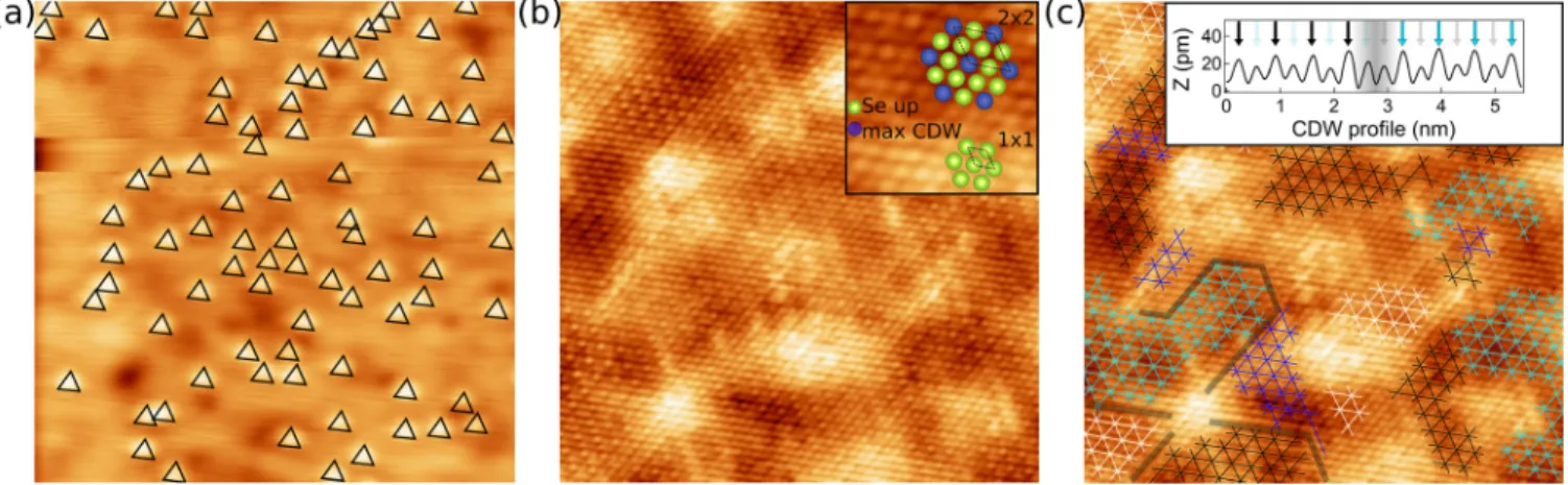
FIG. 1. (a) 17× 17 nm2constant current STM images of the 900◦C -grown 1T -TiSe
2crystal showing the intercalated-Ti defects (black
triangles), Vbias= −1 V, I = 0.2 nA. (b) Constant current STM image at −0.1 V bias voltage and 0.2 nA current set point of the same region
as (a) showing the CDW charge modulation and its perturbation by the presence of Ti defects. The inset presents an eye guide of the 2× 2 and 1× 1 charge modulations. Green spheres correspond to Se atoms of the topmost layer (Se up) and the blue ones to the maxima of the 2 × 2 charge modulation (max CDW). (c) Same STM image as (b) with added meshes highlighting the different CDW domains. Four colors have been used to differentiate between the four possible kinds of modulations that are phase shifted to each other. The gray lines show examples where CDW phase slips occur. The inset shows a height profile through an atomically abrupt CDW phase slip.
DFT model calculations were performed using the plane-wave pseudopotential code VASP [24,25], version 5.3.3. Projector augmented waves [26] were used with the Perdew-Burke-Ernzerhof (PBE) [27] exchange correlation functional. The cell size of our model was 28.035 ˚A × 28.035 ˚A. The 1T -TiSe2 surface was modeled with two
layers and the bottom Se layer fixed. A Monkhorst-Pack mesh with 2× 2 × 1 k points was used to sample the Brillouin zone of the cell. The parameters gave an energy difference convergence of better than 0.01 eV. During structural relaxations, a tolerance of 0.03 eV/ ˚A was applied.
Figure 1(a)presents filled-state STM images recorded at −1 V of the 1T -TiSe2 surface of a high Ti-doped 1T -TiSe2
crystal grown at 900◦C. Bright defects are clearly seen and correspond to Ti atoms intercalated in the vdW gap of the pristine 1T -TiSe2atomic structure [23]. The defect density is
2.57± 0.22% as extracted from statistics made on large STM images and similar to bulk measurements by Di Salvo et al. on a 900◦C-grown crystal [1]. Thus, even if the densities of Ti defects estimated from our STM images mainly account for Ti intercalation in the first vdW gap, they are representative of the bulk Ti-doping density.
In a recent study, it has been shown that the defect density associated with low-doped 1T -TiSe2samples does not affect
the long-range CDW order [28]. For the highly doped crystal and looking at regions with high density of intercalated Ti atoms, atomically resolved STM images (representing the electronic density) near the Fermi energy [Fig. 1(b)] show that the CDW is locally completely absent (bright regions). Approximately 50% of the 1T -TiSe2surface clearly exhibits
short-range CDW charge modulation following the well-known 2× 2 commensurate pattern [see inset Fig. 1(b)] in regions associated with low defect density.
Locating the CDW maxima with respect to the underlying Se atomic layer [Fig.1(c)] now reveals a CDW patterning of nanometer size. Several CDW patterns which differ in their phase relationship with the 1T -TiSe2lattice are observed and
correspond to the four possible configurations of a 2× 2 charge modulation. Interestingly, the CDW boundaries in surface areas free of accumulation of intercalated Ti consist of atomically sharp phase slips between adjacent domains [see inset Fig.1(c)] and appear to occur at random positions of the surface with the charge modulation on either side of the phase slip staying commensurate with the underlying lattice. Isolated Ti impurities are mainly observed within domains suggesting that the CDWs emerged around the bright regions [see bottom left of Fig.1(c)] associated with an accumulation of intercalated-Ti defects.
Therefore, our results strongly indicate that the CDW domains patterning originates in a CDW nucleation-growth process from intercalated-Ti agglomerates. Upon temperature lowering, the nucleating CDWs grow and meet at phase-slip boundaries whose sharpness reflects the very short CDW coherence length [6,29].
At first sight, it may be surprising that a commensurate CDW can break into short-range phase coherent domains in the presence of impurities. Indeed, as previously pointed out by Wu and Lieber who observed commensurate CDW domains on another system (Ti-doped TaSe2) [30], a commensurate CDW
phase that is already strongly coupled to the crystal lattice tends to remain unperturbed by impurity pinning according to a seminal work of McMillan [31]. However, in contrast to McMillan’s Landau theory calculations that describe how a pre-existing charge modulation reacts to the random field introduced by impurities [31], we are concerned here by the emergence of the CDW in with defects already present. Then, the size and arrangement of the CDW domains as well as the domain boundary locations are fully determined by the density of intercalated-Ti nucleation centers, their distribution, and the cooling kinetics.
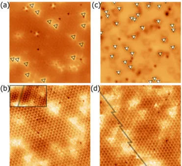
STM measurements carried on 1T -TiSe2 crystals grown
at lower temperature further support our CDW nucleation-growth scenario. Figure2shows 17× 17 nm2constant current
FIG. 2. (a) 17× 17 nm2 constant current STM image of the
770◦C-grown 1T -TiSe2crystal showing the intercalated-Ti defects
(black triangles), Vbias= +1 V, I = 0.2 nA. (b) Constant current
STM image at−0.1 V bias voltage and 0.2 nA current set point of the same region as (a). (c), (d) Same as (a), (b) for the 860◦C-grown 1T -TiSe2 sample. Vbias= −1 V for (c). The gray lines on (b) and
(d) show surface regions where a CDW phase slip occurs. The inset in (b) is a 7.8× 4.5 nm2constant current STM image showing the
presence of a CDW phase slip on the 770◦C-grown sample.
-grown [Figs. 2(c) and2(d)] 1T -TiSe2 crystals. Comparing
both cystals with the 900◦C-grown one for Vbias= ±1 V, we
clearly see that the density of randomly distributed Ti defects [highlighted with triangles on Figs.1(a) and 2(a)and 2(c)] increases with growth temperature. From statistics made on large STM images (not shown), we obtain 0.75%± 0.10% and 1.21%± 0.14% for the crystals grown at 770◦C and 860◦C, respectively, compared to the 2.57%± 0.22% of the 900◦C -grown 1T -TiSe2.
Identically to the highly doped crystal, STM images near Fermi level [Figs. 2(b) and 2(d)] now reveal for both crystals the presence of atomically sharp phase slips of the CDW modulation. Whereas for the lowest doped crystal 60× 60 nm2 images are needed to observe a shift of the
CDW phase [inset Fig. 2(b)], every 17× 17 nm2 image of the 860◦C -grown crystal shows at least one phase slip. This not only demonstrates the close relationship between the CDW domain sizes and the Ti-doping density, but especially reveals that the nucleation-growth mechanism lying behind the CDW formation in the three Ti-doped crystals is the same.
At this stage, we have shown that the CDW can well exist on a very small area and that its pinning to the nucleation centers is energetically more favorable than maximizing a domain size or avoiding phase slips. Also, the coherence length of the CDW is definitely small, suggesting that the strong-coupling theory and a local chemical bonding picture apply [29]. This naturally indicates a local origin of the CDW as driven by a PJT instability [9,32], i.e., not necessitating long-range electronic correlations.
TABLE I. DFT-calculated structural parameters of 1T -TiSe2
with and without intercalated-Ti atom in the vdW gap. Two TiSe6
octahedra separated by one vdW gap are considered: interatomic distances between Se atoms of the topmost layer (dSe-Se), between the
Se neighboring the intercalated-Ti defect d[Se-Se(vdW)], between Ti
atoms along the c axis (dTi-Ti), and between Ti and Se atoms of the
TiSe6octahedra (dTi-Se).
Ti-doped 1T -TiSe2 1T -TiSe2
( ˚A) ( ˚A)
dSe-Se 3.50 3.54
dSe-Se(vdW) 3.64 3.54
dTi-Ti 6.04 6.31
dTi-Se 2.58 2.56
Let us now consider the impact of the intercalation of Ti on the 1T -TiSe2 atomic structure. Table I presents
DFT-calculated, relaxed interatomic distances of the normal phase of 1T -TiSe2with and without one intercalated-Ti atom in the
vdW gap. The impact of the intercalation is rather strong and of the order of magnitude of the periodic lattice distortion. As exemplified in Fig.3, the major effect of the intercalation is the strong decrease (4.3%) of the distance between Ti atoms along the c axis (dTi-Ti) and the symmetric displacement of the
Se atoms surrounding the intercalated-Ti defect. Their in-plane distance [dSe-Se(vdW)] increases by 2.7% whereas the distance
between Se atoms of the topmost layer (dSe-Se) decreases by
1.2% overall leading to elongated (0.8%) Ti-Se bonds (dTi-Se)
of the TiSe6octahedra.
Therefore, the intercalation of one Ti atom in the vdW gap does not favor the CDW instability since it acts against the periodic lattice distortion where 34 of the Ti-Se bonds are shortened [1]. This explains why one isolated Ti defect does not act as a nucleation center for the CDW and also why the CDW charge modulation is highly perturbed just above the intercalated-Ti atom. However, at intercalated-Ti agglomerate edges, the coherent superposition of symmetric Se displacements is expected to induce shortening of the Ti-Se bonds favorable for driving the nucleation of multiple phase-shifted domains in a PJT scenario [9].
Finally, our findings provide insight on the anomalous resistivity peak known to appear around TCDW. Because of
a favorable band configuration with energetically close posi-tioned electronlike and holelike bands, it has been interpreted
FIG. 3. Structural models of 1T -TiSe2as obtained by DFT. Two
TiSe6octahedra separated by one vdW gap are considered (a) pristine
1T -TiSe2, (b) Ti-doped 1T -TiSe2. The amplitude of displacements
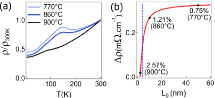
FIG. 4. (a) Temperature-dependent resistivity curves measured on 770◦C (blue curve), 860◦C (dark blue curve), and 900◦C (black curve) grown 1T -TiSe2 crystals. The curves are normalized to
the resistivity measured at room temperature. (b) Evolution of the intensity of the resistivity peak as a function of the CDW domain size. The dashed blue curve indicates the typical value of the effective Bohr diameter of excitons in 1T -TiSe2.
as a reduction of the density of free charge carriers due to electron-hole pairing [10,11]. Its disappearance at lower temperatures is then related to the development of the full CDW gap with unfavorable conditions for the excitonic pairing.
Figure 4(a) shows the relative resistivity ρ/ρ300 K of the
three measured crystals. A maximum is clearly observed for the 770◦C- and 860◦C -grown crystals whereas it is almost absent for 900◦C. In the evolution of the anomalous resistivity peak amplitudes,1as a function of the average domain sizes L
0
extracted from our STM measurements2 plotted in Fig.4(b), there is a dramatic change between the sample grown at 860◦C
1The anomalous resistivity peak amplitude was obtained from
the temperature-dependent resistivity curves after extraction of the semimetallic background using an experimental curve of highly Cu-doped 1T -TiSe2 that does not show the anomalous resistivity
peak.
2L
0 was estimated from STM images by measuring the average
distance between boundaries of CDW domains along the three crystal directions.
and 900◦C despite the only slight diminution of the domain size from 10 to 2.5 nm. It is also interesting to note in Fig.4(b)that a small doping increase from 0.75% (770◦C) to 1.21% (860◦C) is accompanied by a small change in the resistivity but induces a huge reduction of the mean domain size L0.
The abrupt but continuous change of the resistivity maxi-mum with doping can now be understood in terms of exciton confinement within the CDW nanodomains, as discussed for Wannier-Mott excitons in three-dimensional quantum wells [33]. As the typical size of the CDW domain is reduced to 1.5–2 times the effective Bohr diameter of the bulk exciton (dexc = 4.2 nm [34]) [dashed-blue curve Fig. 4(b)],
the electron-hole pairs initially confined as quasiparticles start to break up into individual charge carriers [33]. The result is the disappearance of the exciton-related resistivity maximum for sufficient doping or sufficiently small CDW domains.
The resistivity peak attributed to excitons thus reflects sufficiently long-range electronic correlations in the CDW state. In that sense, the excitonic pairing is an epiphenomenon of the CDW phase transition driven by electron-phonon interaction that allows for the direct coupling of electron and hole bands. Exciton-phonon coupling may thus simply reinforce the CDW state [35], without playing the predominant role in driving the phase transition itself.
To summarize, we report the first observation of short-range phase coherent CDW nanodomains in self-doped 1T -TiSe2.
Our results support a PJT instability as the origin of the CDW patterning. Evidence for confinement effects of electron-hole pairs within CDW domains further provides a coherent picture of the 1T -TiSe2 CDW phase transition and its relation to
excitons.
This project was supported by the Fonds National Suisse pour la Recherche Scientifique through Div. II. We would like to thank C. Monney, C. Renner, and A. M. Novello for motivating discussions. Skillful technical assistance was provided by F. Bourqui, B. Hediger, and O. Raetzo.
B.H. and T.J. contributed equally to this work.
[1] F. J. Di Salvo, D. E. Moncton, and J. V. Waszczak,Phys. Rev. B
14,4321(1976).
[2] E. Morosan, H. W. Zandbergen, B. S. Dennis, J. W. G. Bos, Y. Onose, T. Klimczuk, A. P. Ramirez, N. P. Ong, and R. J. Cava,
Nat. Phys. 2,544(2006).
[3] A. F. Kusmartseva, B. Sipos, H. Berger, L. Forr´o, and E. Tutiˇs,
Phys. Rev. Lett. 103,236401(2009).
[4] Y. I. Joe, X. M. Chen, P. Ghaemi, K. D. Finkelstein, G. A. de la Pe˜na, Y. Gan, J. C. T. Lee, S. Yuan, J. Geck, G. J. MacDougall, T. C. Chiang, S. L. Cooper, E. Fradkin, and P. Abbamonte,Nat. Phys. 10,421(2014).
[5] Y. Yoshida and K. Motizuki, J. Phys. Soc. Jpn. 49, 898
(1980).
[6] M. Holt, P. Zschack, H. Hong, M. Y. Chou, and T.-C. Chiang,
Phys. Rev. Lett. 86,3799(2001).
[7] F. Weber, S. Rosenkranz, J.-P. Castellan, R. Osborn, G. Karapetrov, R. Hott, R. Heid, K.-P. Bohnen, and A. Alatas,
Phys. Rev. Lett. 107,266401(2011).
[8] H. P. Hughes,J. Phys. C: Solid State Phys. 10,L319(1977). [9] M. H. Whangbo and E. Canadell,J. Am. Chem. Soc. 114,9587
(1992).
[10] J. A. Wilson,Phys. Status Solidi 86,11(1978).
[11] H. Cercellier, C. Monney, F. Clerc, C. Battaglia, L. De-spont, M. G. Garnier, H. Beck, P. Aebi, L. Patthey, H. Berger, and L. Forr´o, Phys. Rev. Lett. 99, 146403
(2007).
[12] C. Monney, G. Monney, P. Aebi, and H. Beck,New J. Phys. 14,
075026(2012).
[13] G. Monney, C. Monney, B. Hildebrand, P. Aebi, and H. Beck,
[14] J. van Wezel, P. Nahai-Williamson, and S. S. Saxena,Europhys. Lett. 89,47004(2010).
[15] T. E. Kidd, T. Miller, M. Y. Chou, and T.-C. Chiang,Phys. Rev. Lett. 88,226402(2002).
[16] M. Porer, U. Leierseder, J.-M. M´enard, H. Dachraoui, L. Mouchliadis, I. E. Perakis, U. Heinzmann, J. Demsar, K. Rossnagel, and R. Huber,Nat. Mater. 13,857(2014).
[17] S. Hellmann, T. Rohwer, M. Kall¨ane, K. Hanff, C. Sohrt, A. Stange, A. Carr, M. M. Murnane, H. C. Kapteyn, L. Kipp, M. Bauer, and K. Rossnagel,Nat. Commun. 3,1069(2012). [18] T. Rohwer, S. Hellmann, M. Wiesenmayer, C. Sohrt, A. Stange,
B. Slomski, A. Carr, Y. Liu, L. M. Avila, M. Kall¨ane, S. Mathias, L. Kipp, K. Rossnagel, and M. Bauer,Nature (London) 471,490
(2011).
[19] E. M¨ohr-Vorobeva, S. L. Johnson, P. Beaud, U. Staub, R. De Souza, C. Milne, G. Ingold, J. Demsar, H. Schaefer, and A. Titov,Phys. Rev. Lett. 107,036403(2011).
[20] U. Chatterjee, J. Zhao, M. Iavarone, R. Di Capua, J. P. Castellan, G. Karapetrov, C. D. Malliakas, M. G. Kanatzidis, H. Claus, J. P. C. Ruff, F. Weber, J. van Wezel, J. C. Campuzano, R. Osborn, M. Randeria, N. Trivedi, M. R. Norman, and S. Rosenkranz,
Nat. Commun. 6,6313(2015).
[21] H. H. Weitering,Science 285,2107(1999).
[22] X. L. Wu and C. M. Lieber,Science 243,1703(1989). [23] B. Hildebrand, C. Didiot, A. M. Novello, G. Monney, A.
Scarfato, A. Ubaldini, H. Berger, D. R. Bowler, C. Renner, and P. Aebi,Phys. Rev. Lett. 112,197001(2014).
[24] G. Kresse and J. Hafner,Phys. Rev. B 47,558(1993). [25] G. Kresse and J. Furthm¨uller, Phys. Rev. B 54, 11169
(1996).
[26] G. Kresse and D. Joubert,Phys. Rev. B 59,1758(1999). [27] J. P. Perdew, K. Burke, and M. Ernzerhof,Phys. Rev. Lett. 77,
3865(1996).
[28] A. M. Novello, B. Hildebrand, A. Scarfato, C. Didiot, G. Monney, A. Ubaldini, H. Berger, D. R. Bowler, P. Aebi, and C. Renner,Phys. Rev. B 92,081101(R)(2015).
[29] K. Rossnagel,J. Phys.: Condens. Matter 23,213001(2011). [30] X. L. Wu and C. M. Lieber,Phys. Rev. B 41,1239(R)(1990). [31] W. L. McMillan,Phys. Rev. B 12,1187(1975).
[32] I. B. Bersuker, The Jahn-Teller Effect (Cambridge University Press, Cambridge, 2006), p. 616.
[33] Y. Kayanuma,Solid State Commun. 59,405(1986).
[34] T. Pillo, J. Hayoz, H. Berger, F. L´evy, L. Schlapbach, and P. Aebi,Phys. Rev. B 61,16213(2000).
[35] V.-N. Phan, K. W. Becker, and H. Fehske,Phys. Rev. B 88,