HAL Id: hal-00015306
https://hal.archives-ouvertes.fr/hal-00015306
Submitted on 24 Mar 2006
HAL is a multi-disciplinary open access
archive for the deposit and dissemination of
sci-entific research documents, whether they are
pub-lished or not. The documents may come from
teaching and research institutions in France or
abroad, or from public or private research centers.
L’archive ouverte pluridisciplinaire HAL, est
destinée au dépôt et à la diffusion de documents
scientifiques de niveau recherche, publiés ou non,
émanant des établissements d’enseignement et de
recherche français ou étrangers, des laboratoires
publics ou privés.
X-ray standing wave study of CdTe/MnTe/CdTe(001)
heterointerfaces
Jean-Claude Boulliard, Bernard Capelle, Stéphane Gualandris, Alain Lifchitz,
Joel Cibert, Serge Tatarenko
To cite this version:
Jean-Claude Boulliard, Bernard Capelle, Stéphane Gualandris, Alain Lifchitz, Joel Cibert, et al..
X-ray standing wave study of CdTe/MnTe/CdTe(001) heterointerfaces. Journal of Applied Physics,
American Institute of Physics, 1997, 81 (3), pp.1173-1179. �10.1063/1.363901�. �hal-00015306�
X-ray standing wave study of CdTe/MnTe/CdTe(001) heterointerfaces
J. C. Boulliard,a)B. Capelle,b)S. Gualandris, and A. Lifchitz L.M.C.P., Tour 16, case 115, 4 Place Jussieu, 75252 Paris Cedex 05, France J. Cibert and S. Tatarenko
Laboratoire de Spectrome´trie Physique, CNRS et Universite´ Joseph Fourier-Grenoble, B.P.87, 38402 Saint Martin d’He`res Cedex, France
~Received 11 June 1996; accepted for publication 21 October 1996!
The x-ray standing wave method is used to investigate some crystallographic features of the first stages of growth of ultrathin pseudomorphic MnTe~001! strained layers buried in CdTe on CdTe~001! substrates. Experiments with 004 and 113 reflecting planes show evidence of the presence of both MnTe clusters and diluted CdMnTe alloy.
@~!#
I. INTRODUCTION
The physical properties of semiconductor strained het-erostructures are strongly dependent on the morphology of interfaces~abruptness and roughness! and on the presence of faults ~dislocations, twins, etc.!. Complementary studies are necessary to identify how a given interface can deviate from a perfect one, due to segregation,1to interdiffusion after the growth of the interface,2or during its growth itself,3or to the existence of two dimensional ~2D! or 3D islands reflecting the surface morphology when switching the molecular beams on or off.4 The lateral scale of these deviations is a key parameter, and each experimental method will check the in-terface at different characteristic length scales. For example, for optical studies of excitons confined in a quantum well,4 the lateral scale is defined by the coherence length of the exciton, and the interface will be called smooth if it exhibits only 2D islands, 1 monolayer thick, wider in the interface plane than the exciton size. If these islands are of the order of the exciton size, the interface is called rough since this size island gives rise to a broadening of the exciton optical line due to thickness fluctuations of the quantum well. If the lat-eral scale is even smaller, however, these fluctuations are averaged out and the line is sharp again; then the interface is called pseudo-smooth. These different morphologies have been clearly identified in III–V quantum wells grown under various conditions. The x-ray standing wave~XSW! method is well known to be very sensitive to the position and the order~or disorder! of very thin layers ~less than a monolayer to several monolayers!.5–8We report here on the application of this method to ultrathin MnTe layers grown in CdTe~001! by molecular beam epitaxy. The results will be compared to high resolution transmission electron microscopy~HRTEM! of MnTe layers in CdTe~see Ref. 9! and to a magneto-optic study ~enhanced Zeeman effect! of CdTe-CdMnTe quantum wells.3
In the following sections we describe the XSW method and the experimental setup; the results are reported in Sec. III and discussed in Sec. IV.
A. Principle of the x-ray standing wave method
The XSW method is used to determine the localization of atoms in volume or on a surface. According to x-ray dy-namical theory,5–7 the interaction between the x-ray and a crystal leads to the following result: when the crystal is at a Bragg diffraction position, interferences occur between the incident and the diffracted beam leading to a standing wave field with nodal and antinodal planes parallel to the diffract-ing planes, hkl, and havdiffract-ing the same period, dhkl. When the crystal is rocked through the reflection domain, from lower to higher angles, the positions of the node and antinode planes are shifted inwards by dhkl/2. Thus, the fluorescence
yield of atoms, which depends on the intensity of the x-ray standing wave field, is very sensitive to the atom position. An XSW experiment consists of simultaneously recording the rocking curve and the fluorescence yield of ‘‘impurity’’ atoms~here a thin buried layer!. It determines the position of atoms with respect to the bulk diffracting planes with a good precision, typically within several hundredths of Å. The in-formation is along the normal to the diffracting planes: when they are parallel to the interface ~or the surface!, an XSW experiment gives the vertical position of atoms above the interface; with tilted reflections@like 220 for a ~100! surface#, it gives lateral information~see Ref. 10 for details!.
1. Fluorescence yield and structure
The normalized fluorescence yield is given by~see Ref. 8 and references therein!:
Y~Q!511uj~Q!u212uj~Q!uFhkl cos@c~Q!
22pPhkl#, ~1!
where uj~Q!u2 is the reflectivity and C~Q! the phase of the reflected wave. The Phkl and Fhkl parameters are,
respec-tively, called the coherent position and the coherent fraction. These are related to the Fourier component, with respect to the h diffraction vector, of the atomic distribution, r(z),
a!Electronic mail: [email protected]
b!Also with: LURE, bat. 209D, Centre Universitaire Paris-Sud, 91405 Orsay
along the normal to the diffracting planes ~defined with the nhkl vector!: Fhklei2pPhkl5 *r~z!ei2phnhkl dz *r~z!dz 5 *r~z!ei2pz/dhkl dz *r~z!dz . ~2!
In the case of one atom position, the coherent position is equal to ds/dhkl, where dsis the position of the atom relative
to the diffracting planes and dhkl the diffracting plane spac-ing. In the general case of several atomic sites, Fhkl and Phkl
are given by:
Fhkl5~12DSD!
A
F
(
i fhkli sin~2pPhkli !G
2 1F
(
i fhkli cos~2pPhkli !G
2 ~3! and tan~2pPhkl!5 (ifhkl i sin~2pP hkl i ! (ifhkl i cos~2pP hkl i !, ~4!where Phkli is the ‘‘average’’ coherent position of the i site
~perpendicularly to the hkl plane!. Since the value of the
coherent position, Phkl, is given modulo 1, we will choose,
in the following parts, the Phkl value in [email protected], 0.5#
in-terval. When it is necessary, we will introduce the physical position ~divided by dhkl!, called Dhkl, deduced from Phkl.
We have the relation Dhkl5Phkl1m, where m is an integer
number. ~12DSD! is the random static disorder, which takes into account the percentage of studied atoms which are quasi-randomly distributed, i.e., which cannot be reduced to one average position. The fhkl
i
factor takes into account the disorder, some crystallographic characteristics of the site, and the thermal agitation. It is given by:
fhkli 5DDWi Ahkli hi. ~5! Thehiparameter is the percentage of the i site and DDWi is a Debye–Waller type factor including thermal agitation and static displacements~due to crystalline defects! the statistics of which is gaussian. Its expression is:
DDWi 5exp~2Mhkli ! 5exp~22p2si2/d hkl 2 !5exp~2Bi/4d hkl 2 !.
The Ahkli factor is a geometrical factor which is intro-duced when a site is asymmetrical.
II. EXPERIMENTAL ARRANGEMENT A. Two-axis spectrometer
The experimental setup, installed at the beam line D25B-DCI of the LURE ~Orsay! is a double-crystal spectrometer with horizontal axes to preserve the polarization properties of the synchrotron radiation. This double spectrometer con-sists of two goniometric holders: the first one with the mono-chromator and the second one with the microrotation device and the sample. The reflectivity is measured by means of a scintillation counter ~NaI crystal!. The fluorescence is de-tected with a Si~Li! solid state detector. The angular posi-tioning of the sample and its measurement is achieved by means of an electronic feedback loop between the rotation device ~a lever arm rotated with a piezoelectric transducer!
and the measurement device~a linear capacitive sensor!. The dynamic angular precision is better than 0.01 arcsec. Long term thermal drifts~typically 1 arcsec per hour! are estimated and corrected by periodically recording rapid rocking curves. An experiment consists of several tens of step by step scans through the rocking curve angular domain. The entire setup is controlled by a microcomputer and an integrated software, especially designed for XSW tasks~see Ref. 11!.
B. Analysis of data
Data consist of two sets of arrays~one for fluorescence and one for reflection curve! of several scans. The first array contains the rocking curves and the second one the integrated fluorescence signals from three regions of interest: the first region is the fluorescence peak, the two others, located on each side of the peak, allow the determination of the back-ground which is then subtracted. The rocking curves are checked and then added and corrected for the intensity de-crease. We proceed in the same manner for the fluorescence data. After normalization, the final curves can be fitted. In order to take into account the intrinsic instrumental function, imperfections of the sample and/or of the monochromator, the calculated rocking curves are convoluted with a gaussian curve which is also used for the fit of the fluorescence curve.
C. Monochromators
In order to record precise data, the x-ray incident beam must provide a beam with an angular divergence smaller than the studied rocking curve width and with low harmonic contamination. In order to minimize dispersion, we choose a monochromator such that the distance between its diffracting planes, dh8k8l8, is equal or close to the distance, dhkl, of the
studied reflection on the sample.
Two monolithic grooved four-reflection monochroma-tors have been used in this study: the first, the second, and the fourth reflections are symmetric, the third one is asym-metric ~the principles of this type of monochromator have been previously described in Ref. 11!. The first monochro-mator uses Ge311. Its asymmetry angle for the third reflec-tion is,a516°. The second monochromator uses Si220 with
a510° for the third asymmetric reflection. The Ge311
deliv-ers a beam with a wavelength near 1.7 Å: the 933 harmonic is not detectable. The wavelength of the Si220 has been cho-sen smaller, around 1.2 Å.
D. Sample features
Studied samples consist of CdTe-MnTe heterostructures grown by molecular beam epitaxy on 5 mm square, well-oriented @60.3° from ~001!#, CdTe substrates. They were etched and de-oxidized in a Br-methanol solution and loaded under dry nitrogen into the epitaxy chamber where they were annealed at 340 °C under a Cd flux. A CdTe buffer layer
~;1000 Å! was then deposited at 340 °C under Cd-rich flux
in order to smooth the surface. Then 5 monolayers~MLs! of CdTe were grown at 320 °C, followed by the MnTe thin layer grown at the same temperature~320 °C! under slightly Te-rich conditions. Finally, a 50-Å-thick CdTe cap layer was grown.
The space group of CdTe is F4¯3m; it crystallizes in the zinc-blende~sphalerite! structure, with a cell parameter, a0, equal to 6.481 Å. Bulk MnTe has the NiAs structure ~hex-agonal!, but, when deposited on CdTe ~001!, the MnTe has the same structure as CdTe, with a lattice parameter, as ex-trapolated from bulk Cd12xMnxTe~Ref. 12! or measured on
thick layers, equal to 6.34 Å.
Two samples have been studied: 0.7 ML of MnTe was deposited on sample No. 1, and 2 ML on sample No. 2. These MnTe coverages are deduced from calibrations of the growth rate of thick MnTe layers as measured by the fre-quency of reflectivity high energy electron diffraction
~RHEED! intensity oscillations, monitored immediately
be-fore the growth of the two samples and in the same condi-tions. From previous studies, the precision is better than 10%.
III. RESULTS
A. Experimental conditions
Two sets of experiments were performed on each sample: the first experiment used the Ge311 monochromator
~l51.702 Å! and the CdTe004 symmetrical reflection. The
second experiment~performed several weeks later! used the Si220 monochromator ~l51.113 Å, l51.244 Å, l51.273 Å! and the CdTe113 symmetrical tilted reflection. For the 113 reflection, additional experiments have been performed after a 180° rotation of the samples: these 113 and 1¯1¯3 re-flections had been studied in order to detect a possible asym-metry of the surface.
Before XSW study, topography experiments were per-formed. For both samples, we get the same type of pictures showing that the crystal is bent and that inhomogeneities are present. For XSW studies, we selected parts of the samples that are as homogeneous as possible. Since the disorder is taken into account in our data analysis by a gaussian curve, we chose parts of the sample with symmetric experimental rocking curves. The size of the selected parts is typically equal to a quarter of the sample surfaces. Note that better
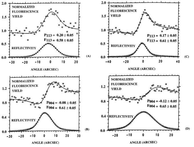
FIG. 1. Experimental points and fitted curves for reflectivity and Mn fluorescence yield.~A! Sample No. 1, 113 reflection, l51.244 Å. ~B! Sample No. 1, 004 reflection,l51.702 Å. ~C! Sample No. 2, 113 reflection, l51.237 Å. ~D! Sample No. 2, 004 reflection, l51.7
rocking curves and topographies are usually obtained with Cd0.96Zn0.04Te substrates: here we chose pure CdTe sub-strates in order to have simpler heterostructures ~nominally they contain only pure CdTe and MnTe!.
B. XSW results
Two 004 and two 113 XSW experiments were per-formed on sample No. 1. Three 004 and three 113 experi-ments were performed on sample No. 2. Examples of results and fits are given in Fig. 1. No difference has been detected between 113 and 1¯1¯3 results. The average Phkl and Fhkl
experimental values are shown in Table I.
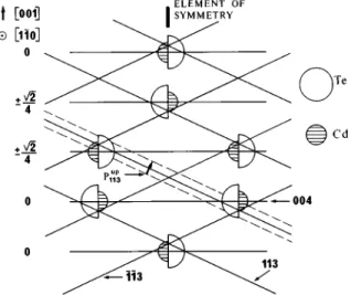
It may be pointed out that, for the 004 reflection, the Cd and Te atom positions are in the diffracting planes but, for the 113 reflection, there are two different atomic positions, hereafter called up and down, and the diffracting planes run near the middle of these atomic positions ~Fig. 2!. A p/2 rotation around the @001# axis inverts these positions: if we have, for example, Cd atoms at the up position for ~113!, they occupy the down position for ~1¯13!. For a given CdTe crystal and an 113 reflection, three cases might be consid-ered: the first is when the Cd atoms occupy the up positions
~and the Te atoms the down positions, consequently!, the
second when the Cd atoms occupy the down positions and the third when the crystal is of poor quality and exhibits the two preceding cases simultaneously ~antiphase domains!. Moreover, when 113 XSW results are analyzed, another point is the choice of the origin for the Phkl value. Three pertinent origins might be chosen; there are the up or the
down positions or the one amidst both these positions. We have chosen the down position as origin of the 113 reflection experiments. So we get ~for atoms of the bulk substrate!
P113down50 and P113up 50.25 ~Fig. 2!. Both cases, Cdup2Tedown and Cddown2Teuphave been considered in the analysis of the data since the position of diffracting planes changes. The fitted P113 value variation, from one case to the other, is approximately equal to 0.025. The calculated Mn atom posi-tions have always been found near the up position. Since in MnTe, the Mn atoms occupy the same sites as the Cd ones we conclude that the samples are of the Cdup–Tedown case
~Fig. 3! ~see the complete demonstration in Sec. IV A 1!.
IV. DISCUSSION
In Sec. IV A we assume that the interface is abrupt with a layer-by-layer growth of pure MnTe on CdTe, and vice-versa. In a first step the experimental distances will be com-pared with theoretical values ~Sec. IV A 1! and the agree-ment between the different Phkl ~and the corresponding
Dhkl! values will be checked. In a second step, the Fhkl val-ues will be analyzed ~Sec. IV A 2!. In Sec. IV B, in order to explain the rather low F004values, models of nonabrupt in-terfaces, implying diffusion and/or terrace nucleation, will be tested.
A. Abrupt interface model
1. Elastic model of MnTe: Analysis of Phklparameters
We first evaluate the distance P004that we might detect with usual simple models. For coherent growth of the epitax-ial MnTe layer on CdTe,9 the MnTe has the same lateral lattice parameter as bulk CdTe, hence the layer has an in-plane isotropic strain equal to exx5ey y
5~a0 CdTe2a 0 MnTe!/a 0 MnTe52.2231022~a 0 CdTe and a0 MnTe are the fcc lattice parameters!. We may now estimate the vertical
@001# component of one MnTe buried layer. For several
lay-ers, the classical elastic model might be used without any hesitation. Although this model might be questioned for a single monolayer, we may use it in order to get upper
esti-FIG. 2. Schematic illustration of a CdTe~001! surface. Side view along
@11¯0#. Geometrical representation of Pup113. On the left size, the positions along@11¯0# are reported.
FIG. 3. Schematic representation of Mn average position~sample No. 1! deduced from the P113and P004experimental values. solid lines: Mn posi-tion. Dashed lines: Cd or Te lattice posiposi-tion.
TABLE I. Fhkland Phklparameters extracted from XSW data.
P004 P113 F004 F113 Sample No. 1 0.7 ML 20.0860.02 0.2060.02 0.6160.05 0.5860.05 Sample No. 2 2.0 ML 20.1260.02 0.1760.02 0.6560.05 0.6160.05 4/7
mation of the P004parameter. The stress being null perpen-dicular to the surface we have szz505c11ezz
1c12exx1c12ey y, from which we get:
ezz522
c12 c11
a0CdTe2a0MnTe a0MnTe .
The MnTe compliance coefficients are not known but those of CdTe and Cd0.5Mn0.5Te~See Ref. 13! have been measured and it has been found that the c12/c11 ratio does not signifi-cantly vary. The Mn position along the vertical z axis ~here parallel to@001#! with the origin on the diffracting planes, in comparison with the Cd one is then:
dMn5d0MnTe~11ezz! 5d0 CdTe
S
11d0 MnTe2d 0 CdTe d0CdTeD
3~11ezz!'d0 CdTeF
12a0 CdTe2a 0 MnTe a0MnTeS
112 c12 c11DG
50.95dCd,where d0MnTe5a0MnTe/4 and d0CdTe5a0CdTe/4. So, the D004value is here equal to 0.95~and P004520.05!.
Another model, which has been suggested for thin InAs layers in GaAs,14 is based on the hypothesis that the buried MnTe layer has the same behavior as in a homogeneous alloy. In other words the Mn–Te bond is constant in length but can rotate. We get:
dMn5
S
2~a0 CdTe!2 8 13 ~a0 MnTe!2 16D
1/2 '0.934dCd. Here, D00450.934 and P004520.066.In sample No. 1, the experimental D004 experimental value, equal to 0.9260.02 ~P004520.0860.02!, is a little low but seems in quite good agreement with the value of the second model.
Concerning sample No. 2, we can estimate the 004 Mn distance from its experimental P004value in the hypothesis that there are two perfectly organized layers with the same spacing ~and the same Debye–Waller factor!. Let us define
Phkl i
the coherent position of the ith monolayer. The position of a second layer is given by P004
2 53P 004 1
. From the experi-mental value, P004520.12 ~which is an average over the two monolayers! we get P004
1 520.0660.01. This last value would be in very good agreement with the second model.
Additional information may be obtained when compar-ing the P004 and P113 results for each sample. We have pointed out that 113 XSW is sensitive to the fact that there are two atomic sites, labeled up and down in Fig. 3. If we assume that the Mn atoms sit only at the up positions~which will have to be ascribed to the Cd site!, then the site is on an axis of symmetry and we can relate the P113value to the P004 one. With the P113origin on the down position, we obtain:
P1135P113 up
1@cos~u!d004/d113#P004, ~6! where u525.24° is the angle between the @001# and @113# directions. So we get:
P1135P113 up10.75P
004 ~here P004 is negative!. For sample No. 1 we calculate P11350.19 ~from the ex-perimental P004! and we measure P11350.2060.02 ~Fig. 3!. In the same manner, for sample No. 2 we calculate
P11350.157 and measure P11350.17060.02.
This agreement shows that there is no presence of Mn atoms on the down sites~‘‘antisites’’!. One can notice that a mixing of 113 up and down positions for Mn would give a
Phkl intersection out of the axis of symmetry ~Fig. 2!. The
P004would be insensitive to the up and down position mix-ing but the 113 experiment would detect two positions: the presence of Mndown would decrease the P113 value and the triangulation of the Phkl would give a point out of the axis of
symmetry.
2. Analysis of the Fhklparameters
We will now discuss the F113 and F004 values of each sample. Let us remember that the Fhkl parameters@formula
~3! and ~5!# depend on the Phkl
i positions of Mn atoms, on
the random static disorder ~12DDS!, and on parameters
fhkli 5 DDWi Ahkli hi, where DDWi is a Debye–Waller type fac-tor,hithe percentage of atoms at site i, and Ahkli , a geometri-cal factor, taking into account the asymmetry of site i. It is readily seen that a discussion of Fhkl values needs more hy-potheses than one about the Phklvalues. We first assume that the random static disorder is negligible. Indeed HRTEM ex-periments on similarly grown MnTe buried layers9have not detected any significant rate of faults which could explain a significant value of the random static disorder. We will also assume that the asymmetry of the site is not important ~i.e.,
Ahkli >1! and can be included in the Debye–Waller factor:
the distortion from symmetry might be estimated to be close to the parameter misfits as suggested by the work of Balzarotti et al.12on Cd12xMnxTe alloy. Moreover, since the
Phkl are more or less compatible with 1 ML on sample No. 1
and 2 ML on sample No. 2 we will not consider, in a first step, the presence of parts of additional layers. Then the co-herent fraction is reduced to the Debye–Waller factor~which is supposed to be isotropic! for sample 1, and depends on the Debye–Waller factor and the coherent positions for sample 2.
The maximum value of the Debye–Waller factor might be estimated under the hypothesis that the Mn thermal vibra-tions are close to the ones of the Cd atoms in the CdTe substrate. Since we have BCd51.71,15the calculated Debye– Waller factor are e2MCd0045 0.85 and e2MCd1135 0.89. We will first discuss the F004. It is readily seen that the experi-mental value on sample 1 ~0.6160.05! is much lower than the above estimated Debye–Waller factor. Considering sample number 2 we can extract the Debye–Waller factor if we take into account the fact that there are two monolayers
@formula ~3!#. With P004
1 520.066, we get e2MCd
004
5 F004/0.9255 0.70 6 0.06, which is smaller than the value calculated for thermal vibrations. Such a low value has been already reported for adsorbate structures ~see Ref. 16 and references therein, for example! but seems difficult to justify for our buried layers. Concerning the F113 values one can
expect that their value must be higher, since d113 is greater than d004. It is not the case and so a higher lateral disorder is evidenced.
In conclusion it is readily seen that the hypothesis of perfect MnTe layers, which accounts for the measured Phkl
values, cannot explain the low Fhkl results without assuming
exceedingly large defect densities. In Sec. IV B we will in-troduce interface models which might explain the experi-mental F004values without the recourse to structural defects.
B. Nonabrupt interface models
In the preceding sections we have discussed our results under the hypothesis that the 0.7 ML sample has only one Mn position~incomplete ideal perfect MnTe monolayer! and the 2 ML sample, two Mn positions ~ideal MnTe double monolayer!. We will now assume that terrace nucleation and exchange of Cd/Mn atoms across the interface appear during the growth of the MnTe thin layer ~Fig. 4!. Terrace nucle-ation is suggested by the observnucle-ation9of a roughness increas-ing with the thickness of MnTe layers ~these layers were thicker than in the present study!; the atom exchange was described in Cd12xMnxTe heterostructures with x around 0.3.3 We have first tested two extreme models, one with roughness only and one with dilution only.
1. Roughness
In the first model we consider that the Mn is organized in MnTe islands, several monolayers thick. In order to esti-mate the minimum F004value we will assume that each layer has the same lateral size~i.e., the same coverage! and that the
Phkl parameter for one perfect layer has the value deduced
from the rotation bond model ~note however that this is in-deed the case where the bulklike elastic model should better apply!. Let us call, as above, P004
i
the Mn 004 position of the
ith layer. We have P004
i 5(2i21)P
004 1
and P004
1 520.066. The F004values, without the Debye–Waller factor, are suc-cessively equal to F004>0.91 for two layers, F004>0.73 for
three layers, and F004>0.61 for four layers. We might con-clude that a MnTe island model needs at least three layers, but in this case the P004value ~P004>20.2! becomes lower than the experimental one and therefore this extreme model must be rejected. Moreover it is easily seen that derived models ~with variations of the layer percentages! give equivalent conclusions.
2. Dilution
In the second model we assume that there are one or several full layers of Cd12xMnxTe laterally homogeneous
alloy. The value of the lattice parameter is known to vary linearly with x ~Vegard’s law!. Hence the insertion of a single monolayer of Cd12xMnxTe will shift the Mn atoms
within this layer by x P004 1
, where P004 1
is the above value in MnTe, and shift the atoms sitting on it by 2x P004
1 ~this de-scription should hold well for dilute alloys, and probably less for concentrated alloys where the formation of Mn pairs, triads, and larger clusters should introduce some disorder!. We see at once that if sample No. 1 actually contain a mono-layer of Cd0.3Mn0.7Te due to a rapid diffusion within the surface layer, we should measure a larger value of P004,
P004520.04, and F004 close to 1 since it would comprise only the Debye–Waller contribution as in Sec. IV A. Refer-ence 3 suggests that we have several layers of Cd12xMnxTe alloy, with x resulting from a complete intermixing, during the growth of the interface, between the ~just incorporated! surface layer and the monolayer being grown. P004and F004 are easily calculated for a given composition profile xi and the resulting P004i : P004i 52
(
j,i xjP004 1 1x iP004 1 .If necessary, an integer number has to be added in order to remain in the @20.5, 0.5# interval. All reasonable composi-tion profiles ~uniform xi or profiles from Ref. 3! lead to larger P004than for the nominal profile~Sec. IV A! and F004 values close to 1.
3. Roughness and dilution
From the two preceding models, and from the abrupt interface model, we must conclude that: ~a! in the abrupt interface model, the values of P004are correct but we cannot explain the low F004values; and~b! the formation of clusters or 3D islands~or roughness! decreases the values of P004and
F004; if we assume that all Mn atoms are incorporated in 3D islands, the calculated F004parameter can be decreased down to the experimental value, but the calculated P004value is too low;~c! the dilution of MnTe into a Cd12xMnxTe alloy
in-creases P004; if we assume that all Mn atoms are incorpo-rated in laterally homogeneous Cd12xMnxTe alloy layers,
then the calculated P004parameter is larger than the experi-mental one, and the F004is close to 1.
Actually a better agreement can be found by assuming that both islands and alloy coexist @Fig. 4~d!#. We have checked this for sample No. 2 which exhibits a larger F004 value ~i.e., better ordering!. We assume that the MnTe layer is composed with one complete MnTe monolayer covered
FIG. 4. Schematic of the models used for the 2 ML sample~No. 2!, ~a! ideal 2 ML,~b! islands, ~c! alloy, ~d! mixed ~open circles: Mn, solid: Cd!.
with MnTe pyramidal islands and Mn diluted atoms. For example, the respective area of each layer of the pyramidal island corresponds to the ratio 4:2:1. With a quantity of di-luted Mn atoms equivalent to 0.5 ML and pyramidal islands the bases of which occupy 28% of the surface, we get the experimental P004value~P004520.12! with F00450.8. This last value agrees with the experimental value corrected from the thermal vibrations ~F00450.765!. Similar morphologies
~pyramidal MnTe islands and diluted Mn atoms! may also
account for the 004 experimental values of sample No. 1. Of course the exact morphology of these islands is not known. Moreover, a precise calculation should take into account strain relaxation at the island edges, and the existence of clusters in the alloy.
We may note that such morphologies would agree with both the results of HRTEM on MnTe buried layers,9 which reveal that roughness tends to increase during the growth of MnTe under Te excess, and those of Zeeman effect of exci-tons in CdTe-Cd12xMnxTe quantum wells, which reveal that
an exponential alloy profile is found when the whole struc-ture, with x50.2 to 0.4 is grown under Cd excess. Similar Zeeman effects are found for nominally pure MnTe barriers,17followed by the growth of a CdTe quantum well, but we have to keep in mind that in this case Zeeman effect of confined excitons tests the existence of an exponential tail of Cd12xMnxTe only in the low concentration part of the sample, i.e., the nominally pure CdTe quantum well grown under Cd excess. Samples entirely grown under Te excess seem to exhibit both rougher interfaces ~broader optical lines!, and lower Zeeman effects indicating a smaller dilution of Mn into the CdTe quantum well.18 It is worth noting that while magneto-optics studies are mainly sensitive to the presence of isolated Mn atoms~i.e., the decrease of the num-ber of Mn pairs correlated by nearest-neighbour antiferro-magnetic interaction! in the low-concentration part of the sample, on the contrary the present XSW study reveals the presence of MnTe clusters, whatever their shape, in MnTe-CdTe heterostructures.
V. CONCLUSION
The 004 and 113 XSW study of 0.7 and 2 MnTe mono-layers buried in CdTe~001! give coherent position values
which agree with those expected for MnTe coherently strained to CdTe. If we assume perfect interfaces, a slightly better agreement is found if we assume that the strain is accommodated by bond rotation only, than if we apply bulk elastic coefficients. However, the experimental coherent frac-tion values Fhkl lead suspect that the interfaces are not abrupt. The vertical Mn distribution on the 2 ML sample is compatible with a crude model including one MnTe layer and a mixing of MnTe islands and diluted Mn atoms
~CdMnTe alloy!. The 0.7 ML sample seems to contain MnTe
islands together with CdMnTe alloy.
ACKNOWLEDGMENTS
We would like to thank A. Jeanne-Michaud for the drawing of the figures.
1J. M. Moison, C. Guille, F. Houzay, F. Barthe, and M. Van Rompay, Phys. Rev. B 40, 6149~1989!.
2D. To¨nnies, G. Bacher, A. Forchel, A. Waag, and G. Landwehr, Appl. Phys. Lett. 64, 766~1994!.
3W. Grieshaber, J. Cibert, J. A. Gaj, Y. Merle d’Aubigne´, and A. Wasiela, Phys. Rev. B 50, 2011~1994!.
4
R. K. Kopf, E. F. Schubert, T. D. Harris, and R. S. Becker, Appl. Phys. Lett. 58, 631~1991!; D. Gammon, B. V. Shanabrook, and D. S. Katzer, Phys. Rev. Lett. 67, 1547~1991!.
5B. W. Batterman, Phys. Rev. A 133, 759~1964!. 6
B. W. Batterman, Phys. Rev. Lett. 22, 703~1969!. 7
A. Authier, Acta Crystallogr. A 42, 414~1986!. 8J. Zegenhagen, Surf. Sci. Rep. 18, 199~1993!.
9P. H. Jouneau, A. Tardot, C. Feuillet, H. Mariette, and J. Cibert, J. Appl. Phys. 75, 7310~1994!.
10
A. Taccoen, C. Malgrange, Y. L. Zheng, J. C. Boulliard, and B. Capelle, Acta Crystallogr. A 50, 497~1994!.
11J. C. Boulliard, B. Capelle, D. Ferret, A. Lifchitz, C. Malgrange, J. F. Pe´troff, A. Taccoen, and Y. L. Zheng, J. Phys.~France! I 2, 1215 ~1992!. 12
A. Balzzarotti, N. Motta, A. Kisiel, M. Zimmal-Starnawska, M. T. Czyzik, and M. Podgorny, Phys. Rev. B 31, 7526~1985! and references therein. 13P. Maheswaranathan, R. J. Sladeck, and U. Debska, Phys. Rev. B 31, 5212
~1985!.
14O. Brandt, K. Ploog, R. Bierwolf, and M. Hohenstein, Phys. Rev. Lett. 68, 1339~1992!.
15V. T. Bublick and S. S. Gorelick, Kristall und Teknik 12, 859~1977!. 16G. E. Franklin, S. Tang, J. C. Woicik, M. J. Bedzyck, A. J. Freeman, and
J. A. Golovchenko, Phys. Rev. B 52, 5515~1995!. 17
F. Kany, H. Ulmer, and G. Feuillet, International Conference on Semicon-ductor Heteroepitaxy, Montpellier, 1995.
18S. Kuroda, K. Kojima, K. Kobayashi, A. Saito, K. Takita, K. Uchida, and N. Miura, Fourth International Workshop on Semimagnetic Semiconduc-tors, Linz, 1994; Mater. Sci. Forum 18, 615~1995!.