Development of Three-dimensional Passive
Components for Power Electronics
by
Padraig J. Cantillon-Murphy
B.E. University College Cork (2003)
Submitted to the Department of Electrical Engineering and Computer Science in partial fulfillment of the requirements for the degree of
Master of Science in Computer Science and Engineering at the
MASSACHUSETTS INSTITUTE OF TECHNOLOGY May 2005
@
Massachusetts Institute of Technology 2005. All rights reserved.Author ... . .... . . .
Departge4( of Electrical Ehgineering dd Computer Science May 13, 2005 Certified by... Accepted by... Chairman, . . . . .... ... .. . . ... .. .... ... . . . . David J. Perreault Emanuel E. Landsman Associate Professor of Electrical Engineering and Computer Science Thesis Supervisor
Arthur C. Smith Department Committee on Graduate Students
MASSACHUSETrTS INSTITUTE OF TECHNOLOGY
OCT 2
1
2005
Development of Three-dimensional Passive Components for
Power Electronics
by
Paidraig J. Cantillon-Murphy
Submitted to the Department of Electrical Engineering and Computer Science on May 13, 2005, in partial fulfillment of the
requirements for the degree of
Master of Science in Computer Science and Engineering
Abstract
As component and power densities have increased, printed circuit boards (PCBs) have taken on additional functionality including heatsinking and forming constituent parts of electrical components. PCBs are not well suited to these tasks. A novel fabrication method is proposed to develop an enhanced circuit board fabrication approach which overcomes this problem. This method uses a photoresistive scaffold and subsequent metallization to realize the proposed structures. These structures are suitable as heatsinks, inductor windings, busbars and EMI shields among other applications.
Thesis Supervisor: David J. Perreault
Title: Emanuel E. Landsman Associate Professor of Electrical Engineering and Computer Science
Acknowledgments
I would like to thank a number of people without whom this achievement would not have been possible. Firstly, to Dave for investing so much time and effort in me over the past two years, for being patient throughout and for always encouraging me to go the extra yard. To Professor Kassakian; for affording me the opportunity to work at his laboratory, for always making me feel welcome and for having the common touch.
Thank you to all the lads at L.E.E.S.; for making me feel at home, never getting mad, always helping me out and never letting me down. Sh6inte agus p6g mo th6in! Special mention should go to Josh, who was especially tolerant of my stupdity. To Vivian, for everything only Vivian can do and to Wayne for the help and advice. A special acknowledgement is due to Kurt Broderick for his moments of inspiration.
I want to thank Aubs, (for teaching me how to dream) Ciar and Gobs, Maur and Bill, and Anne and Paddy, (for all the support you give, in many, many ways) and, in particular, Mamie...because you'll never let my feet get off the ground!
Finally Eamonn and Micheil cause you're the greatest friends a brother could wish for; and Dad and Main; for everything. You're the greatest!
And finally, finally to St. Teresa of Avila because:
"Despite the uncertainties and the labor which every attempt to interpret reality entails - not only in the sciences, but also in philosophy and theology - the paths of discovery are always paths towards truth. And every seeker after truth, whether aware of it or not, is following a path which ultimately leads to God, who is Truth itself."
16"
a"
4
~
His Holiness Pope John Paul II.Address to the Pontifical Academy of Sciences. November 8, 2004.
Contents
1 Introduction 13
1.1 Three-dimensional Patterning . . . . 14
1.1.1 The Scaffold Technique . . . . 15
1.2 Current Technology . . . . 16 1.3 Circuit Structures . . . . 17 1.4 Thesis Organization. . . . . 18 2 Preparation 19 2.1 Overview. . . . . 19 2.2 Pouring Equipment . . . . 20 2.3 Preparation . . . . 21 3 Thermal Analysis 25 3.1 Ancillary Issues . . . . 26
3.2 The Effect of Vias . . . . 31
3.3 Theoretical Analysis . . . . 32
4 SU-8 Processing 39 4.1 SU-8 Applications to 3D PCBs . . . . 39
4.1.1 Substrate Preparation . . . . 41
4.1.2 SU-8 Pouring and Pre-bake . . . . 42 7
4.1.3 Exposing SU-8 . . . . 43 4.1.4 Developing SU-8 . . . . 44 4.2 Higher Structures . . . . 47 4.3 Failure Mechanisms . . . . 49 5 Metal Deposition 51 5.1 Sputtering . . . . 51 5.1.1 Improving Adhesion . . . . 52 5.1.2 Sputtering Procedure . . . . 53 5.2 Electroplating . . . . 55
6 Pinfin Heatsink Testing 59 6.1 Optimized Pinfin Heatsinks . . . . 59
6.2 Testing . . . . 61 6.3 Results Analysis. . . . . 63 6.4 Investigation of Anomalies . . . . 64 7 Conclusions 71 7.1 Accomplishments . . . . 71 7.2 Future work . . . . 73
A Thermal Resistance of a Flat 2 Sq. Inch Board. 75
List of Figures
1-1 A simplified illustration of a scaffold fabrication approach. . . . . 15
1-2 Laser direct structuring. . . . . 17
2-1 The sandwich structure assembled for pouring . . . . 22
2-2 Photograph of the apparatus used for pouring . . . . 24
3-1 Typical maximum power dissipation curve . . . . 26
3-2 Equivalent thermal resistor network for the TO-220 heatsink . . . . . 28
3-3 Investigation of Ancillary Issues related to heatsink optimization . . . 30
3-4 Investigation of increasing heatsink area with vias . . . . 32
3-5 Investigating the effect of vias on heatsinking . . . . 32
3-6 Thermal IR profile of Board 1 at an input power of 4.5W . . . . 34
3-7 Results of modelling investigation comparing flat and viaed heatsinks 36 4-1 Highlighting the increased functionality associated with recent PCB technology . . . . 40
4-2 SU-8 Process Flowchart . . . . 41
4-3 Pre-bake heating profile for the 80Opm SU-8 process . . . . 43
4-4 Comparing microscopic appearances of underdeveloped and correctly developed 800pm SU-8 pins . . . . 45
4-6 An example of "drift" failure in the SU-8 strucures observed during the PEB stage . . . . 50 5-1 An example of adhesion failure after electroplating. . . . . 53 5-2 An example of successful copper seed-layer deposition by sputtering. . 54 5-3 The electroplating bath was contained in a teflon container. . . . . . 56 5-4 Illustration of sulfuric acid bath electroplating with active copper
elec-trodes. ... ... 56 5-5 An example of successful electroplating of the board from Fig. 5-2. . . 58 6-1 Hexagonally packed cylindrical pinfins . . . . 60 6-2 Results of the investigation of pinfin heatsinks . . . . 62
6-3 The effect of a second electroplating step on three of the boards was investigated. . . . . 65 6-4 Examination of Board 0 after the second plating step. . . . . 66 6-5 Adhesion failure between the two copper layers of Board 0 after the
second plating step. . . . . 67 6-6 Failure mechanisms in the electroplated copper of Board L. . . . . 67 6-7 "Creep" of electroplated copper lifts the SU-8 from the substrate. . 68
List of Tables
3.1 Details of boards used to investigate ancillary issues. A check mark
indicates that the board has a specific characteristic. . . . . 29
3.2 Details of boards used to investigate the effect of vias . . . . 31
4.1 Recipes for varied SU-8 structure heights. . . . . 47
5.1 Correlation between copper weight and thickness. . . . . 53
5.2 Operating conditions for Cu plating. . . . . 55
6.1 Details of boards used to investigate pinfin heatsink optimization. A check mark indicates that the board has a specific characteristic. Board J is a simple flat heatsink. . . . . 61
Chapter 1
Introduction
As component and power densities have increased, printed circuit boards (PCBs) have taken on additional functionality. This includes acting as the principal means of conducting heat away from electronic components (heatsinking), carrying high power and high frequency signals (busbars and transmission lines) and forming constituent parts of electrical components (e.g. forming printed windings for "planar" inductors and transformers). Conventional circuit board technology is not well suited for re-alizing this additional functionality, and is increasingly imposing limitations on the achievable size and performance of electronic equipment.
In order to better understand the work carried out here, it is useful to explore the standard industry approach to PCB fabrication. A PCB comprises a sheet of insulating material (typically laminate) with a thin layer of copper foil (typically between 18 and 180 pm thick) bonded to one or both sides and etched to form a desired interconnect pattern [1, 2]. Connections between the two sides are formed by drilling holes in the board and plating them through. Multi-layer boards are fabricated by stacking up multiple board layers and connecting them appropriately. The resulting sandwich structure of thin copper layers and laminate is highly effective for providing medium-density interconnections among components at low cost (though cost tends to rise rapidly as the number of layers is increased).
While the structure of conventional PCBs is effective for mounting and intercon-necting circuit components, other functions important in modern electronic circuits are not well served by this structure. For example, the PCB structure is not very effective at transferring heat from components to the environment [1], necessitating the use of large circuit board areas and/or mounted heatsinks to meet thermal re-quirements. Similarly, conventional PCB technology is not ideal for forming busbars or the windings of magnetic components. As a result, power density suffers because of the geometric constraints imposed by the planar printed traces. In these and other regards, conventional PCB technology is imposing limitations on the achievable size and performance of electronic equipment. These limitations are becoming more important as component and power densities continue to increase.
This thesis investigated an enhanced circuit board fabrication approach that pro-vides three-dimensional patterning of one or both of the outside layers of circuit boards, and enables greatly improved realization of these structures and functions. With further work, this three-dimensional circuit board (3DCB) technology has the potential to overcome the limitations of existing PCB technology at low cost, while preserving much of the conventional manufacturing framework. It is anticipated that 3DCB technology will benefit a wide range of electronics applications, particularly those where size and power density are important, including power supplies, radio-frequency and microwave circuits, and portable electronics.
1.1
Three-dimensional Patterning
To realize three-dimensional surface patterning, this technique uses photolithogra-phy in conjunction with commercially-available ultra-thick photoresists. Such three-dimensional patterning techniques have been widely explored for fabricating micro-electromechanical (MEMS) devices [6], and can be readily adapted to the present application. One available photoresist system that has been exploited in the past
and that we propose to use here is SU-8 [9, 10]. This negative1 photoresist can be used to fabricate structures with heights exceeding 1 mm and aspect ratios of more than 18 [9], thus providing feature heights on par with typical circuit components and feature resolution as good as that found in most PCB designs. The approach used to fabricate these structures makes use of a "scaffold" technique.
1.1.1
The Scaffold Technique
(C)
(b)
Figure 1-1: A simplified illustration of a scaffold fabrication approach. (a) The surface layer of the circuit board is coated and patterned to reveal only desired conductor areas. (b) Ultra-thick photoresist is deposited, exposed, and developed to form a three-dimensional scaffold. (c) A thin seed-layer of conductor is deposited and patterned. (d) A heavier copper layer is electroplated over the seed layer, completing the structure.
While the scaffold technique could be used in a number of distinct ways, high-lighted in Fig. 1-1 is the easiest and most cost effective approach. A thin photoresist is first applied to the circuit board and patterned, leaving only desired conductor areas exposed (Fig. 1-la). Ultra-thick photoresist is then deposited, exposed, and developed to form a three-dimensional scaffold (Fig. 1-1b). Next, the entire surface (including the scaffold) is covered with a thin conductive seed layer and patterned (Fig. 1-1c). A much heavier layer of conductor is then electroplated over the seed-layer, completing 'In negative photoresists, the mask exposes the areas which will be retained after development.
the three-dimensional structure (Fig. 1-1d). A key step in this process is depositing and patterning the seed-layer which is accomplished by sputtered metal deposition.
The proposed scaffold fabrication approach is particularly advantageous when a structure having a high exposed surface area is desired (e.g., for heat sinking or to reduce high-frequency resistance). A key advantage of all of the methods used is that they are compatible with existing PCB fabrication processes and are fundamentally inexpensive.
1.2
Current Technology
There have been a number of patents granted for work completed on three-dimensional circuit structures in recent years, although none have been found to replicate the scaffold technique discussed here. Alford et al. [3] fabricated a three-dimensional inductor coil on a semiconductor substrate by sequential deposition and etching of photoresistive layers and by electroplated metal deposition to produce a multi-loop inductor coil. Hirsch and Lin's [5] invention is a method for fabricating a high-aspect ratio, freestanding microstructure using SU-8 photoresist. Cylindrical cavities with aspect ratios of 8:1 are claimed. Finally, Warren [4] describes a technique for patterning electroless plated metal on a polymer substrate. The substrate is then complexed with a noble metal compound, such as palladium, selectively irradiated to form the desired conductor pattern, before etching to reveal the desired conductor pattern. Electroless plating is used to form the final metal pattern.
While not using photolithographic methods, there is a company in Germany fab-ricating 3D device contours with the use of laser technology. "LPKF Laser & Elec-tronics AG"2 have developed a process that uses laser-sensitive plastic substrates to fabricate laser-written circuit patterns directly from computer generated layout. The substrate consists of an injection-molded plastic doped with a metal-based organic
2
LPKF Laser & Electronics AG, Osteriede 7 D-30827, Garbsen, Germany. (http://www.lpkf.com)
compound that undergoes a local physiochemical reaction upon laser activation. This exposes metal atoms along the intended circuit path. Finally, the actual circuitry is deposited in an electroless plating step. The technique is highlighted in Fig. 1-2. While the technique allows trace resolution down to 100 pm with 150 pum spacings,
it uses a non-standard substrate. Circuit trace
Circuit trace
Carrier- -
-Step 1. Step 2. Step 3.
Laser
Injection - Bath
Mold
Figure 1-2: Laser direct structuring, a new way of creating molded interconnect devices, uses laser energy to activate those portions of injection-molded carrier that correspond to the deposited circuitry.
1.3
Circuit Structures
The scaffold technique enables the fabrication of a wide range of valuable three-dimensional structures. For example, pin-fin heatsinks can be directly fabricated as part of a circuit board with the proposed technology (Fig. 1-1d). One would ex-pect this heatsink to greatly improve heat transfer to the surrounding air and allow for a corresponding reduction in the board area needed for this function. In many contemporary PCB designs, large copper plane areas are dedicated solely to heat sinking. Accordingly, this application was explored in some detail. While 1 mm
pin-fin heatsinks were successfully fabricated and tested, the devices failed to show any improvement over a comparable plane area heatsink, due to cracking of the electro-plated copper at the recessed corners of the pin-fin structures. However, a successful technique to fabricate high-aspect ratio SU-8 structures has been successfully demon-strated and with further investigation it is possible that these pin-fin structures can show significant improvement over planar heatsink areas.
1.4
Thesis Organization
The thesis is divided into five chapters, this first one being the introduction. Chapter 2 details the preparation and setup work undertaken before the scaffolding fabrication process could begin. In Chapter 3, an investigation of power applications is presented. This focusses on heatsink structures and examines the performance of viaed heatsinks. This chapter offers the pretext for the fabrication of pinfin heatsink fabrication using scaffolding.
The next chapter deals with the SU-8 processing from deposition through to de-velopment. In Chapter 4, the process of metal deposition is discussed while Chapter 5 outlines the tests undertaken on the pinfin heatsinks fabricated using the scaffolding process. Finally, the conclusions of Chapter 6 are intended to synopsize the work undertaken and offer direction for any subsequent investigations.
Chapter 2
Preparation
2.1
Overview
The first step in manufacturing the proposed three-dimensional (3D) structures is creating a scaffold. In our experimental process, this is achieved by pouring SU-8 onto an FR4 substrate, pre-baking it to drive out the solvent and then patterning the poured structure through photolithography. Here we describe the apparatus and methods developed to create pre-baked SU-8 structures of relatively uniform thickness (up to 1mm) that are suitable for subsequent photo-processing.
In order to achieve effective pouring of the SU-8 photoresist onto the FR4 sub-strate, a simple mechanical structure has been designed and constructed. This struc-ture facilitates the controlled pouring of SU-8 onto the substrate and the subsequent pre-bake process.
Obviously, the most critical requirement of the structure is to prevent the pho-toresist from leaking onto the hotplate on which it rests. To this end, a four-layer sandwich is arranged consisting of the hotplate, the substrate and teflon and alu-minum rings.
The apparatus consists of a square hotplate, measuring 10 inches in length, onto which is clamped an aluminum plate, with 16 bored and tapped screw-holes. This
was thought to be a more practical approach to simply boring into the hotplate. The interface between the plate and sheet was thermally greased and clamped firmly. up to four unclad FR4 substrates rest on the sheet, such that there is a screw hole adjacent to, but not covered by, each substrate corner. The FR4 substrates were purchased from the Injectorall Corp. Each square board measures 3 inches in length and 120 mil in thickness. Enclosing each substrate is a square ring of teflon® which fences in the outer perimeter of the FR4 without overlapping the screw-holes in the aluminum plate. Finally, each teflon® ring is clamped in contact with the substrate by a square aluminum ring on top. Each of these aluminum rings has 4 bored corner holes allowing it to be screwed into the aluminum baseplate.
This sandwich structure, detailed in Fig. 2-1 and photographed in Fig. 2-2 is effective in restricting all of the poured SU-8 to an enclosed square of FR4 substrate, measuring 2.5 inches in length.
2.2
Pouring Equipment
A Dataplate® digital hotplate has been purchased from Omega Engineering Inc. This 100 sq. inch hotplate is equipped with a timer, automatic turn-off and "ramp per hour" settings as well as closed-loop plate temperature control.
The aluminum baseplate has been cut to fit flush over the hotplate top surface. Each of its tapped screw holes were chosen to fit a 5/8 inch 10-32 size screw which links it to the aluminum rings. The hotplate was thermally greased before the baseplate was clamped onto its corners.
The baseplate is also been drilled so that beneath the center of each FR4 sub-strate was a narrow vacuum vent. Each of the vent-passages leads to the edge of the baseplate where sealed, male-pipe to barbed adapters are attached to each. Flexi-ble vacuum tubing feeds to 4 ball valves with Swagelok1 tube fittings. Finally, each
'Available from McMaster-Carr at http://www.mcmaster.com
valve connects to a 4-way manifold which passes to the vacuum pump. The pump is an oilless vacuum pump from Gast Manufacturing Inc., capable of supplying a 10 psi vacuum. It is connected to the mains via a heavy-duty switch with an indicator lamp. This vacuum assembly is necessary to ensure uniform clamping of the substrate to the levelled hotplate. Unlevel substrates would result in significant height variations in the SU-8 structures after development. The vacuum is also important in the initial alignment of the substrate within the teflon® and aluminum clamps.
The 4 square teflon® ring-clamps were fabricated using an abrasive water-jet cutter. Teflon® was chosen in this application because of its minimal moisture ab-sorption and low friction coefficient2. The diameter of the teflon® ring-clamps was such as to fence in the outer perimeter of the FR4 substrate without overlapping the screw-holes.
The 4 square aluminum ring-clamps, also cut using water-jet, were of slightly longer length to overlap with the underlying baseplate screw holes. These were drilled at each corner with a 10-32 size through-hole, so that the aluminum ring could be fastened to the baseplate, clamping the substrate and the teflon® ring in between.
2.3
Preparation
The room where pouring took place was fitted with UV-light filters, effective below wavelengths of 500nm, to avoid interference with the subsequent SU-8 exposure. The room was also equipped with a dehumidifier system, which maintained humidity below 45%, regardless of ambient conditions. This was to counter the adverse effect of high humidity on SU-8 adhesion, which is well understood [7]. The preparatory rinsing cleaning and drying of the FR4 substrates was conducted in an acid-hood. A 2-hp air compressor with a detachable air-gun has been purchased to allow rapid drying of the substrates after ethanol and deionized water rinsing. Finally, a controllable
2
http://www.dupont.com/teflon/af/unique.html
Figure 2-1: Drawing detailing the sandwich structure used to effective SU-8 pouring. Legend Aluminum Ring Teflon Ring Substrate Aluminum Plate Hotp late
high-temperature oven is used to remove any excess moisture still present after blow-drying. The oven temperature is maintained at 180'C.
Critical to attaining structures of uniform height is correct levelling of the hotplate. This is achieved with the aid of a "bulls-eye" level. However, it is difficult to achieve perfect levelling at the micron scale. So the structure heights (e.g. 800pm and 1mm) achieved reflect the average height over the entire board rather than the exact height of each individual structure.
Chapter 3
Thermal Analysis
In the investigation of fabrication techniques suitable for use in power electronics, it was decided that heatsinking structures would be the application to explore. The dis-sipation of heat from both passive and active components has long been an important focus of the power electronics industry. Heat dissipation has become more challeng-ing in light of increaschalleng-ing power densities. Coupled to this is the critical emphasis on low cost devices which further complicates the challenge. This chapter outlines the experimental testing and modelling of viaed boards investigate the effect of increased viaed cooling area on heatsink performance.
Demonstration of the approach is focussed primarily on heat removal from a TO-220 device package. This package is ubiquitous in the power electronics sector, as well as the general electronics area, housing, for example, diodes, MOSFETs and, power resistors. A practice of manufacturers has been to include a curve in the component's datasheet [20], similar to that in Fig. 3-1. The curve relates steady-state power dissipation in the device to the required cooling area. This assumes that the designer has allocated enough space on either the bottom or top surface of the PCB to allow effective device cooling. Clearly, this constrains the designer's use of space. The cooling effect, due almost entirely to convection, increases as the area is made larger. So an intuitive approach to increasing area would be to use a PCB with plated vias
3 S2 LLI I-I- -e 00 0.2 04 0.6 0. 1
2c 'OPPER MOUNTING PAD AREA (n )
Figure 3-1: Maximum power dissipation curve for the SOT-223 power MOSFET from
Fairchild Semiconductor [20]
so as to increase the effective cooling area and promote increased convective airflow. Elementary mathematical analysis shows that the vias' radii should be less than twice the total board thickness to result in an increase in the overall cooling area. This is seen by comparing the curved surface inside the via to the area of a circle with the via's radius. To test this hypothesis, a series of experimental tests and supporting analytical study were undertaken.
The general procedure for experimental testing was to fasten a TO-220 resistor to the heatsink structure and observe temperature rise as the input power is varied. However before any particular conclusions could be drawn regarding the effectiveness of various techniques, it was thought prudent to investigate some ancillary issues which might give rise to future concern.
3.1
Ancillary Issues
The first of these effects is radiative heat transfer from the PCB surface. This was analyzed by spraying the heatsink surface with black paint. Therefore, should there be significant radiated heat transfer from the heatsink surface to the ambient envi-ronment, then this would be reflected in a lower device operating temperature for
Top Qli
R~~rrna
-
2S34
BZ _____ _____ __I
Stil Airthe blackened surface. Since the general Stefan-Boltzmann expression for radiative heat transfer from a surface shows that transfer is linearly proportional to the fourth power of temperature, radiative effects are not expected to be significant [14].
The second consideration investigated at this point is the effect of the direction of unforced airflow over the board surface. This is investigated by turning the entire board heatsink on its side so that any flow which was parallel to the surface of the flat board is now perpendicular to the surface of the turned board. Again, any significance would be evident in the temperature measured at the thermocouple.
Finally, the effect of greasing the interface between the resistor and the board was investigated by comparing thermocouple readings with and without greasing.
At this point it should be noted that the position of the thermocouple for the purpose of temperature measurement is critical to the understanding of the heat flow that takes place. In this initial investigation, two thermocouples were positioned on the heatsink, on either side and half way between the resistor's center and the board's edge. The average reading of the two was recorded in each case. However, upon some consideration, it is evident that a more efficient heatsink (yielding lower device temperature) can result in a higher temperature on the board surface, away from the device, for a given power level. This is because a lower thermal resistance to conduction across the board will have a correspondingly lower temperature drop
across it if the power source is constant.
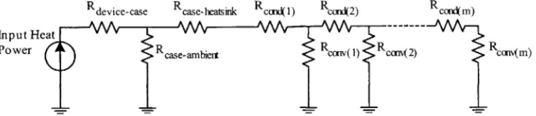
It is helpful to think of this in terms of circuit theory, where the power input corresponds to a current source and the temperature drop across a thermal resistor is analogous to a voltage drop across an ohmic resistor [21]. The situation investigated might be modelled in terms of a finite convective and conductive thermal network as shown in Fig. 3-2. Clearly, the resistance between the resistive device of the TO-220 and the package case, as well as the convective resistance between the case and the ambient environment are beyond immediate control. However, if the board's conductive resistance is increased, then the temperature at a point half-way between
Rdevice-case R ase-hetsink Rcand1) Rcond(2) Rcond(m)
Power Rcase-ambient Rc (1 Rconv(2) Rconv(m)
Figure 3-2: Equivalent thermal resistor network for the TO-220 heatsink. The horizontal thermal resistances, Rcond, reflect conduction through the board, while the vertical resistors,
Rconv, reflect heat removal through convection from the board.
the heat source and the board edge will show an increase, and not a decrease, in temperature.
A more intuitive thermocouple position is on the TO-220 case. A thermocouple
on the case will record a lower temperature for a more effective heatsink. In the initial investigation described below, the thermocouple is on the heatsink, so that higher temperature (on the board away from the TO-220) signifies more efficient heat transfer. Subsequent tests measure performance with the thermocouple fastened to the TO-220 case. Note that there is a slight difference in temperature between the plastic case of the TO-220 and the tab. However, this difference has never been seen to exceed 2% of the absolute tab temperature and can not be considered significant since all measurements are made in the same manner. Therefore, for ease of attachment to the device, the thermocouple was epoxied to the plastic case rather than the tab itself.
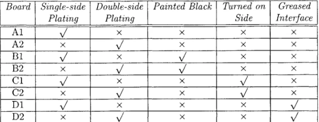
The test boards are 2 single layer PCBs with 2 square inches of 1 oz. plated copper on one or both sides and central plated holes for attaching TO-220 5.1Q resistors. Each board has an inline arrangement of 0.06 inch diameter vias, positioned in two rectangular areas surrounding the resistor, as illustrated in Fig. 3-4. Four such boards were ordered and the boards were labelled A to D for clarity. The details of each are outlined in Table 3.1.
Board B is is used to investigate the effect of radiation, while the boards labelled
C and D are used to examine board orientation and the effects of greasing the
Board Single-side Double-side Painted Black Turned on Greased
Plating Plating Side Interface
Al x x x x A2 x V x x x
B1
x x xB2
x x x C1 x x %x C2 x x N_ x DI V_ x x xV
D2 x x x _ _Table 3.1: Details of boards used to investigate ancillary issues. A check mark indi-cates that the board has a specific characteristic.
package interface respectively. The A board is used as a benchmark. The number index, 1or 2, refers to whether or not the board is single-side or double-side plated. The results for each board are plotted in Fig. 3-3.
The first clear result is that the effect of radiation is negligible. This is seen by comparing the plots for the A and B boards. These are virtually identical within the bounds of experimental error. Accordingly, radiation is clearly not significant and is not considered further in the analysis.
The plot leads to further interesting results. Since the highest surface temperature is recorded on the C boards with the greased interface, we conclude that this is the most effective heatsink, as reasoned previously. All subsequent investigation was undertaken with the interface between the heatsink and the TO-220 lightly greased. Also, the effect of turning the board is noticeable but not overly significant. This is evident from comparison of results for boards A and D. The effect of the vias is more perceptible if the board is oriented vertically and, while noteworthy, this result is not applicable in a general case since board orientation and airflow direction will vary with the application and ambient conditions. In each case, the addition of plating on the bottom of the board acts to increase the temperature observed for a given input power. As outlined previously, this indicates a more effective method of heat
Investigating Radiative Effects C 80 E 70 60 Topian d ntom-SPlatingt 50
Inveti4nTop Eeating Only
4 90 -- _ _ _ __ _ _ _ __ _ _ _ _ _ 30 E 20 W 1A70 --- A2 -B1 --- B2 20 - -0 1 2 3 Input Power [W]
Investigating Effect of Greasing
E 801
70 Top and T Bottom Plt
> Plating-60 -6-30 -40 10 - 0-0 1 2 3 Input Power [W]
nvestigating Board Orientation
80
Top and Bottom Plating E
70---> 60
.0 50
CD U-,--- Top Plating
_- 40
tOnly
t;30 .D 20 1-A1 --- A2 --- D1 ---- D2 T 10 0 1 2 3 Input Power [WMBoard I Total Number of Vias
1 0
2 92
3 109
Table 3.2: Details of boards used to investigate the effect of vias
transfer to the environment, as one would expect with the addition of a high thermal conductivity copper path on the board's underside.
3.2
The Effect of Vias
This preliminary investigation concluded, attention was now turned to the effect on cooling of a viaed PCB. Thermal vias are a frequently used technique to quickly and efficiently transfer heat from the source, usually for conduction to a nearby cooling plane. [16, 17, 18]. This experiment is intended to investigate their effectiveness for convection in the absence of any forced airflow and compare performance with an unviaed PCB over a relatively large cooling area.
To test the efficiency of vias an additional set of circuit boards was employed, with temperature measurements taken at the device case. Each test-board is a single-layer PCB with 4 sq. inches of loz. plated copper. The details of each board are outlined in Table 3.2. The vias on boards 2 and 3 are packed inline and arranged in rectangular squares around the resistor. The arrangement is detailed in Fig. 3-4.
Board 1 has no vias and is used for comparison purposes. Similar to the previous test the input power was increased from zero and the corresponding temperature rise noted. In these tests, however, the thermocouple was epoxied to the TO-220 package itself. As mentioned previously, this proves a more appropriate measurement of performance, where lower case temperature indicates more effective cooling at a given input power level. The results of the test are shown in Fig. 3-5. Board 1 is labelled "No Vias" while boards 2 and 3 are labelled "Low Density Vias" and "High
Figure 3-4: Investigation of increasing heatsink area with vias -100 90 E 80 70 0 60 50 4A
Investigating Via Effects
-NoVias ----Low Density Vias N Vias
.--- High Density Vias
Low Density Via$ High Density Vias
~-t'I
___ _ ___ ____ ___ 30-20 10 0 V---- ----0 1 2 3 4 5 Input Power [W]Figure 3-5: Investigating the effect of vias on heatsinking
Density Vias" respectively. All three boards show remarkably similar results although Board 3 shows slightly improved performance. The reasons for this are explored in the analysis that follows.
3.3
Theoretical Analysis
By way of explaining the experimental data from the test on viaed board cooling, a theoretical analysis was undertaken. This was not an attempt to directly replicate any experimental results with an analytical model. Rather, its aim was to provide an intuitive appendix to the actual results and help broaden the understanding of the data recorded. This analysis draws heavily on the standard tools of heat transfer
theory [14]. Since the goal is not a detailed model but simply a means to better understand the test results, the approach taken is deemed sufficient for this work.
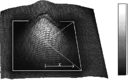
In comparing boards 1, 2 and 3 from Table 3.2, the analysis examines the tem-perature distribution in one dimension along the plane of the PCB. One-dimensional analysis considerably simplifies the complexity of the problem and eases the capacity for an intuitive understanding. The analysis relies on the fin approximation of heat transfer from extended structures. An involved discussion of this theory can be found in any heat transfer text (e.g. [14]) and is not considered here. Suffice to note that the approximation supposes that heat gradient in one direction (x in this case) sustains the heat transfer by conduction internally, while at the same time, there is energy transfer from the surface, principally by convection. The PCB lies in the {x,y} plane such that its edge is parallel to the z axis and the dominant conduction path is along the x axis. The temperature distribution along the y plane, which points into the board, is assumed negligible compared to that along the x axis. This assumption is one that is generally acceptable in a thin board and with the addition of vias, there is no danger of this temperature distribution being significant. Temperature distri-bution along the z axis is not considered either. The infra-red photograph of Board
1, taken at an input power of 4.5W, shows that these approximations are reasonable.
Furthermore, any inaccuracies associated with the method are not considered pivotal to the understanding of the test results.
By application of the fin approximation, the board is decomposed into 4 parallel-connected fins, each an isosceles triangle of height equal to half the board's length. Their tips meet at the board's center so that each triangle has base angles of 45'. and a tip angle of 90'. One such fin is highlighted in Fig. 3-6. The complete "Mathematica"1 source code for the analysis of the boards 1 and 2 is included in Appendices A and B. Since this includes a detailed explanation of all the relevant assumptions associated
1Mathematica is an extensive mathematical and engineering simulation package available from
Wolfram Research, Inc., Champaign, Illinois, USA. (http://www.wolfram.com) The version used in
this analysis is Mathematica 4.1
10PC
AM
Figure 3-6: Thermal IR profile of Board 1 at an input power of 4.5W
with the analysis, it is not examined in depth here.
Suffice to note that each fin is further decomposed into a ladder network cor-responding to Fig. 3-2, where conductive resistance is given by Equation 3.1 and convective resistance by Equation 3.2. In this case, I is the incremental distance of each element in the x direction, kA is the effective product of thermal conductivity (in W/mK) and cross-sectional area in each element, A, is the surface area available for convective heat transfer from each element and h is the coefficient of convective heat transfer from the board.
Rcond = (3.1)
kA 1
Rcon= 1 (3.2)
Fixing the conductive resistance from the device to case and the convective loss from the the case to the ambient, an expression is developed for the case temperature
as a function of input power. Evaluation of the ladder network now allows the curves of Fig. 3-7 to be plotted corresponding to boards 1 and 2. The viaed board shows slightly improved performance, reflecting the actual results of Fig. 3-5. However, the performance of the viaed boards, in both simulation and experiment, depend hugely on h. Its value for a flat board is estimated from the expression relating Reynolds
(Ren) and Nusselt (Nu) numbers in laminar free convection, repeated in [14} and
given in Equation 3.3.
Nu
= 0.54Ren
025 (3.3)The Reynolds number, a dimensionless physical function of board parameters and ambient conditions, relates inertial to viscous flow effects and is estimated from Equation 3.4, where:
g = acceleration due to gravity in in/s 2 T, =surface temperature in K
T= air temperature in K
v = kinematic viscosity of air in m2
/s a = thermal diffusivity of air in m2
/s I = board length in m
gf3[T, -Tol
Ren = (3.4)
Finally, Equation 3.5 relates the Nusselt number to the effective coefficient of heat transfer over the entire board area, where k is the thermal conductivity of the air, dependent on the board's surface temperature.
h =kNu (3.5)
Rise in Tab Temperatuxe above Ambient 60 Board 1 6 0 Board 2 40 20
Input Power in Vatt;
1 2 4 5
Figure 3-7: Results of modelling investigation comparing flat and viaed heatsinks
(350K), leads to a value of 14.35 W/m2
K for h, where the thermophysical properties of air, as a function of temperature, are available from the National Institute of Standards and Technology2
as well as most heat transfer texts[14]. The value of 78*C was chosen as typical of the normal operating temperature in many power electronics applications. Also, since the variations in the thermophysical properties are not significant over temperature compared to the quadratic dependence on board length, this is judged a reasonable approximation. This value, calculated for the case of a flat board, will not be true for a viaed board, so its value is altered, as outlined in Appendix B, to account for this discrepancy and the recorded results for the viaed board.
While the addition of vias to the board results in some improvement in both the experimental and theoretical analysis, it is clear that the effect is minimal and certainly not sufficient to justify it as a design tool in most applications. Also of note is the fact that the addition of vias, while increasing the area available for convective
2
heat dissipation, severely limits the lateral conductive heat path across the board by disrupting the high thermal conductivity copper path that exists on the top surface of the flat board. Accordingly, the arbitrary introduction of more vias will not result in
any significant improvement in performance and instead leads to poorer heat transfer from the source.
Although not a general result, this investigation is interesting in its justification of a physical result. It also provides the motivation to identify fresh techniques of increasing cooling area that will have a significant impact on device temperature. One such approach is a pinfin heatsink, where the vias might be replaced with pinfins on the PCB surface.
Chapter 4
SU-8 Processing
The scaffolding process is thought to be suitable for the fabrication of a variety of structures with applications in the power electronics sector. These include busbars, planar inductor windings, EMI shields and heatsinks. Heatsinking was chosen as the initial avenue of exploration for a number of reasons, but most notably because there exists the possibility of an optimum design exists for specific applications. Also, the techniques applicable to fabricate 3D heatsink structures should be readily applicable to other structures. This chapter outlines the photolithographic procedures of the scaffolding process, from SU-8 deposition through to the development of structures up to 1.2 mm. Apart from the poured deposition step, all of the work took place at the Microsystems Teaching Laboratory (MTL) at M.I.T.
4.1
SU-8 Applications to 3D PCBs
The general target of the PCB application is "vertical wall" structures of up to ap-proximately 1 mm in height and as high an aspect ratio as is feasible (e.g. in excess of 4:1). Such structures will be suitable for heatsinks and many other applications. In keeping with standard practice in the PCB industry, the substrate used is FR4. The board substrate used in these prototypes and experiments measures 9 sq. inches.
Figure 4-1: Highlighting the increased functionality associated with recent PCB technology.
In general, there is a vast amount of vacant volume on the surface of a PCB, be-cause the board packaging will be determined by whatever component stands highest off the board, as shown in Figs. 4-1 (a) and (b). Even in the most recent power con-verters, planar inductors can rarely be made lower than 1mm, leaving at least that much space for exploitation. This is seen in Fig. 4-1 (c). Therefore, the goal of this investigation is to explore structures of SU-8 up to 1mm.
While the current practice is to spin-coat the photoresist onto the substrate, such an approach would not be expected to be commercially viable in this case. Multiple coatings would be required to reach 1mm and there may be concerns relating to the integrity of the bonding between coatings. Therefore a different approach is proposed. Instead of spin-coating, the photoresist is poured onto the substrate with a pipette. Clearly, if we want to accurately measure the poured volume, the SU-8 solution will need to be of relatively low viscosity. The solution selected was SU-8 2005, which
Substrate Pretreat
Pouring
Soft Bake
Expose
Post Exposure Bake (PEB)
Develop
Rinse & Dry
Figure 4-2: SU-8 Process Flowchart
was supplied by the Microchem Corp.1 of Newton, MA. SU-8 2005 is a negative radiation sensitive resist supplied in a 45% cyclopentanone solvent solution[12]. The entire SU-8 process is outlined in Fig. 4-2 and outlined in detail in the following sections.
Following numerous iterations, an effective pouring recipe was eventually arrived upon. This was developed by a combination of references [7, 8, 12], other students' work and the author's experience in the field. The recipe outlined here produced a 800pm layer of cured SU-8 on an area of 6.25 sq. inches. While the overall board area is 9 sq. inches, the bounding teflon ring eliminates some of this.
4.1.1
Substrate Preparation
To begin, the FR4 substrate is rinsed in isopropyl alcohol (IPA) to remove any sur-face dust or contaminants remaining after manufacturing, followed by a rinsing with
1
deionized water. After blow-drying any surface moisture from the surface, it is placed in a temperature-controlled oven at 130C for 30 minutes to remove any remaining moisture or dampness.
Once dry, the surface is micro-roughened to improve adhesion between the sub-strate and the SU-8. This is accomplished by placing the FR4 in an oxygen plasma environment for 10 minutes. The asher, which is a "Plasmod" from the Tegal Corp. is a 100 W, 13 MHz RF device used at 60% of its rated power under a vacuum of 350 mT. The ashing process is critical to achieving satisfactory adhesion between the FR4 substrate and the SU-8 after curing. The process is thought to relate to three principle mechanisms; (i) mechanical keying or interlocking, (ii) molecular forces and dipole interactions and (iii) chemical bonding[19]. These mechanisms contribute ei-ther alone or in combination to produce the necessary bond. The rule of thumb is the higher the surface energy of the substrate, the higher the wettability and the associ-ated improvement in adhesion. To correlate with this theory, a wettability test was undertaken, in order to estimate the relative wettabilities of the ashed and unashed boards. This test, the "Accu Dyne Test", available from Diversified Enterprises2, estimates wettability3 in dynes/cm. The result is that the unashed board was esti-mated at 56 dyne/cm while the ashed board was found to lie above the testing range, which extended to 60 dyne/cm.
4.1.2
SU-8 Pouring and Pre-bake
Once ashing is complete, the substrate is removed immediately to the hotplate where
the SU-8 is poured. It is important to limit the time that the substrate is exposed
to the atmosphere after ashing so as to minimize the ambient moisture that may absorbed.
To make sure that thermal equilibrium is maintained over the entire surface of the
2
Diversified Enterprises, 101 Mulberry Street, Suite 2N, Claremont, NH 03743. 31 dyne/cm = 10-5N/cm.
" Hotplate Temperature
Time in Hours
3 6 9 12 15 18 21
Figure 4-3: Pre-bake heating profile for the 8Opm SU-8 process.
board, the FR4 is preheated to 65'C on the hotplate for 30 minutes before pouring. At this point, 10ml of SU-8 2005 formulation is pipetted onto the board. The SU-8 is prevented from flowing off the substrate by the boundary of teflon around its perimeter. It has been found that a slow pre-bake is critical to the successful expulsion of all the solvent in the SU-8 [12]. Accordingly, the temperature is raised at a rate of 2C per hour for 15 hours, until the temperature reaches 95'C. The temperature is maintained at 95'C for 3 hours before the hotplate is switched off. Again, the board remains on the hotplate until temperature has returned to room level, so that sudden changes in temperature are avoided upon cooling. This usually takes about 2 additional hours. A plot of the entire heating profile is included in Fig.4-3. Now the aluminum clamp can be unscrewed and the teflon clamp carefully prised away. At this point, we immediately begin the exposure process.
4.1.3
Exposing SU-8
It has been shown that high dosages of UV power below 350nm can result in over-exposure of the top portion of the photoresist [12]. Therefore, the 400 ultraviolet mJ/cm2
source4, measured with an i-line (365nm) probe and scope is filtered below 4
350nm using a glass slide filter with a 40% transmission efficiency. This effectively reduces the UV source to about 230 mJ/cm2
and accounts for the long exposure time required: 30 minutes. Placing a transparent film mask over the SU-8 during exposure will allow the subsequent development of the desired three-dimensional pattern. The masks were manufactured by the "Pageworks Company" of Cambridge, MA5 on high resolution 5080 dpi transparent film. The mask is maintained in contact with the pre-baked SU-8 during exposure.
After exposure is complete, the substrate is immediately removed to a hotplate for the post-exposure bake (PEB). Again, it is imperative to minimize the delay in transferring from exposure to PEB and so ensure uniformity in the density of the cross-linking SU-8 chains [9, 12]. The substrate is baked at 65'C for 15 minutes, before being ramped at 180*C per hour to 95'C where it is maintained for an additional 3 hours. Experience has shown that the adhesion between the final SU-8 structure and the FR4 substrate improves with PEB time. The two-step PEB is designed to minimize substrate stress, wafer bowing and resist cracking. After completing the PEB, the board is removed from the hotplate and allowed to cool slowly in air. Again, this limits the stress associated with abrupt cooling. This usually takes 30 minutes,
after which, the development step can begin.
4.1.4
Developing SU-8
After cooling, the SU-8 is placed in a beaker of MicroChem's SU-8 Developer6. De-velopment time will vary, depending on the pattern exposed but is usually between 1 and 1.25 hours for 800pm high structures. The development can be shortened by heating the developer above room temperature, uniform agitation of the beaker and changing the developer solution mid-way through the process. However, careful
at-5PageWorks, 501 Cambridge Street, Cambridge, MA 02141 (http://www.pageworks.com) 6
MicroChem's SU-8 Developer is effectively a solution of standard PM Acetate (Propylene Glycol Methyl Ether Acetate).
tention is paid during the final stages of development to avoid over-development of the structure. This would lead to undercutting of the final SU-8 mold and adhesion failure. The problem of under-development, which is the shown in Fig.4-4, is also to be avoided. To complete the process, it may be necessary to squirt additional developer in areas where the photoresist is slow to etch off. This is particularly the case for intricate structures. A final rinse with IPA followed by a rinse with deionized water completes development. The board can be blow-dried with air to remove any surface moisture that remains.
Figure 4-4: Comparing microscopic appearances of (left) underdeveloped and (right) cor-rectly developed 800pim SU-8 pins
A selection of 800pm SU-8 structures are included in Fig.4-5. Successfully fabri-cated structures include pinfin arrays and inductor windings. These structures exhibit good adhesion to the FR4 substrate, sharp side-wall profiles and excellent material integrity.
Structure Height 800pm
Poured SU-8 Volume 10ml 12ml
Soft Bake time at 95C 3 hrs. 6 hrs.
Exposure Time 30 mins. 35 mins. Development Time 1-1.25 hrs. 1.25-1.5 hrs.
Table 4.1: Recipes for varied SU-8 structure heights.
4.2
Higher Structures
Having completed an initial investigation of structures up to 800pm, the next step was to increase the structure heights. A target was set at 1mm structures. This proved achievable, but required a number of changes from the 800pm recipe. The two procedures are outlined in Table 4.1. The pre-bake process is identical to Fig.4-2 over the first 19 hours. However, for 1mm structures, the plate temperature is maintained at 95*C for an additional 3 hours, in order to expel all the solvent present before returning to room temperature as before. Exposure and development times are also increased as outlined in Table 4.1. While structures up to 1.2mm have been successfully fabricated, it becomes increasingly difficult to expel all the solvent during the pre-bake without the mold becoming so brittle that it cracks on removal from the teflon ring.
Having found the expected linear relation between poured volume of SU-8 and the subsequent structure heights, an attempt was undertaken to quantify this mathemat-ically. Critical to this analysis is the estimation of the densities of SU-8 2005 before and after curing. Since this data was not readily available, it was estimated by mass and volume measurements of the board before and after the pre-bake. The result is
that the density increases from 995.2 kg/m 3
beforehand to 1283.8 kg/M 3
after. The relationship between poured volume and structure height is examined in Equations 4.1 through 4.5, where:
Vpoured= volume of SU-8 poured before pre-bake in m
3
Vcured = volume of SU-8 after pre-bake in m3
mpoured = maSs of SU-8 poured before pre-bake in kg
Mcured= mass of SU-8 after pre-bake in kg
Ppoured= density of SU-8 poured before pre-bake = 995.2 kg/m 3
Pcured= density of SU-8 after pre-bake = 1283.8 kg/m 3
Aboard= board area available for pouring = 0.00403 m2
h = cured structure height in m
As outlined in [12], the solid content of SU-8 2005 is 45% by mass. So assuming all the solvent is expelled during the pre-bake, then the mass decreases to 45% of its original value. Vcured = mcured (4.1) Pcured Vcured Acured * h (4.2) = h = Mcured (4.3) Pcured * Acured h = 0.45 * npoured (4.4) Peured *
Acured
h 0.45 * Vpoured * Ppoured 86.51 * Vpoured (4.5) Pcured * Acured
Estimating Equation 4.5 for 10ml and 12ml leads to theoretical structure heights of 865pim and 1.038mm respectively, which is resonably close to the values measured with a micrometer; 800pum and 1mm respectively. It should be noted, however, that
it is extremely difficult to attain constant structure height over the entire surface due to imperfect levelling of the hotplate prior to pouring. While every effort is made to level the hotplate, through the use of bulls-eye levels, this is only sufficient to ensure an an estimated accuracy of t10ptm.
4.3
Failure Mechanisms
Initially, the most common source of failure during SU-8 processing was due to wet or humid weather affecting the adhesion between the SU-8 and the FR4 substrate. High humidity makes it quite difficult to expel all of the solvent from the SU-8, presumably due to the higher water content of the environment. This results in an epoxy that is very tacky, difficult to expose and does not adhere to the FR4 substrate. The addition of a dehumidifier to the room where the pre-bake took place practically eliminated this effect. However, it is worth noting that the majority of this work took place between the months of October and March, when ambient humidity in Boston is generally low anyway.
Failure to insert the glass slide filter during exposure will result in SU-8 that is extremely tacky and generally the substrate becomes inseparable from the transpar-ent slide mask. If the soft-bake time is too short, then one encounters "drift" of the exposed features during the PEB stage, as shown in Fig.4-6. This phenomenon is thought to result from excess solvent at the SU-8/FR4 interface which was not expelled during the pre-bake, returning to an aqueous state and destabilizing the overhead pattern.
Under-development of the SU-8 structures is an obvious mistake to be avoided. However, after rinsing the board with IPA, it is generally clear with the naked eye whether or not more development is required. Over-development is a more difficult issue to resolve. This requires an understanding of the specific process since more intricate features require more time to develop. Copious squirting of developer into
Figure 4-6: An example of "drift" failure in the SU-8 strucures observed during the PEB stage.
the more hard-to-reach features of the design will help to alleviate the problem of non-uniform development over the board's surface. Over-development generally results in widespread adhesion failure at the SU-8/FR4 interface, which would generally occur in the course of blow-drying the board after development is complete.
Chapter 5
Metal Deposition
Having completed the fabrication of SU-8 structures on FR4, the next step is metal deposition. This takes place in two steps. Firstly, a very thin seed-layer of sputtered metal is deposited on the area as needed, and then, electroplating is used to increase the thickness as desired. There is also the option of patterning the deposited metal for applications such as inductor windings. This chapter details the methods and pro-cesses used in metal deposition on the SU-8 structures described previously. Possible patterning techniques are discussed in Appendix C.
5.1
Sputtering
Sputtering is a process of using a plasma to bombard a metal target and transfer a film of material onto a substrate or onto the component which is to be coated. It is an example of a physical vapor deposition (PVD). An electric field (either AC or DC) is first applied and then Ar ions are accelerated towards the target. When the
Ar ions strike the target, their kinetic energy is transferred to the target material
and particles are ejected. One advantage of sputtering over, for example, electron beam evaporation, is that the Ar ions strike the target as well as the substrate. This can be beneficial for adhesion between the substrate and the deposited material but


![Figure 3-1: Maximum power dissipation curve for the SOT-223 power MOSFET from Fairchild Semiconductor [20]](https://thumb-eu.123doks.com/thumbv2/123doknet/14744560.577737/26.918.304.623.146.355/figure-maximum-power-dissipation-curve-mosfet-fairchild-semiconductor.webp)