Effect of Oxygen on Ni-Silicided FUSI Metal Gate
H.P. YU1, K.L. PEY1,2, W.K. CHOI1,3, D.Z. CHI4, E.A. FITZGERALD1,5, D.A. ANTONIADIS1,5
1
Singapore-MIT alliance, 4 Engineering Drive 3, Singapore 117576
2
School of Electrical & Electronic Engineering, Nanyang Technological University, Nanyang Ave, Singapore 639798
3
Department of Electrical & Computer Engineering, National University of Singapore, 4 Engineering Drive 3, Singapore 117576
4
Institute of Materials Research and Engineering, 3 Research Link, Singapore 117602 5
Massachusetts Institute of Technology, 77 Massachusetts Avenue, Cambridge, MA 02139-66307
Abstract -- Continual evolution of the CMOS technology requires thinner gate dielectric to maintain high performance. However, when moving into the sub-65 nm CMOS generation, the traditional poly-Si gate approach cannot effectively reduce the gate thickness further due to the poly-depletion effect. Fully silicided metal gate (FUSI) has been proven to be a promising solution. FUSI metal gate can significantly reduce gate-line sheet resistance, eliminate boron penetration to channels and has good process compatibility with high-k gate dielectric. In this paper, the effect of oxygen introduced by the process of conventional furnace annealing in FUSI metal gate is investigated.
A 120 nm amorphous Si layer was sputtered on dielectric oxides of various thicknesses grown using a standard oxidation process. Raman spectra showed that the 120 nm thick pre-sputtered amorphous Si recrystallized after annealing in a conventional furnace at 900 °C. Secondary ion mass spectrometry (SIMS) revealed that the annealed Si film contained traces of oxygen which were incorporated into the film during the furnace annealing process. It is suspected that the oxygen was originated from a few ppm of impurities present in the high-purity annealing gas (N2). When a 100 nm of Ni was deposited using a DC sputterer on such sample and was rapid thermal annealed (RTA) at 400 °C to form a fully silicide film, the transmission electron micrograph showed the existence of unreacted oxygen-rich Si layer along the interface of the NiSi/SiO2, leading to areal non-uniformity in the workfunction. It is suggested that the presence of oxygen can effectively retard the Ni diffusion into the Si film during the silicidation process such that the FUSI process is delayed, and the equivalent oxide thickness (EOT) increased as shown by capacitance-voltage (C-V) measurements. The workfunction of Ni-silicided FUSI film determined by C-V measurement on MOS structures was found to increase compared to the as-deposited amorphous Si film (the control sample).
Index Terms -- metal gate, FUSI, Ni silicidation, gate depletion
I. Introduction
As metal oxide semiconductor field effect transistors (MOSFETs) are continuous scaling down to the sub 65-nm-generation technology, it is necessary to reduce the gate insulator thickness to less than 2nm [1]. With the gate insulator scaling, the degradation of performances due to gate depletion becomes serious. For example, poly-silicon gate depletion makes it difficult to reduce the equivalent oxide thickness further. Boron penetration is another major consideration for device scaling. So
there is a strong demand for the reduction of the thermal budget in order to suppress its influence on ultra-shallow junction for 65nm CMOS and beyond. The fully silicided (FUSI) poly-Si gate which shows a metal-like behavior is a promising candidate for gate electrode for solving the problems associated with poly-silicon gates [2]-[4]. Among all the metal material for silicidation, Ni attracts a lot of attention since it has lower Si consumption and better thermal stability.
It was found that, impurities play a very important role in Ni silicide processing. Different dopants such as boron, phosphorus and arsenic [5][6] are widely used to tune Ni FUSI metal gate Workfunction to the band-edge. Some can be used to improve FUSI thermal stability [7]. In addition, in bulk silicide reaction, native oxide at Si wafer interface prevents Ni diffusion and Ni silicide formation [8]. This paper attempts to study the influence of oxygen impurity on the FUSI reaction and its effects on the electrical properties of the NiSi electrode.
II. Methods and experiment
The starting material is 100 mm p-type Si wafer. The wafers were subjected to the standard RCA I and RCA II cleaning processes followed by a dip in a 10% HF solution to remove the native oxide layer. After the oxide removal, the wafers were loaded into a furnace for dry oxidation. Four different samples were prepared with oxide thicknesses of 6nm, 10nm, 15nm and 19nm, respectively. Elipsometer was used to measure the grown
SiO2 thickness. After that, a 120nm amorphous Si layer was
deposited using RF sputterer at a vacuum level 4 x 10⁻⁷ Torr on
the samples. These samples were annealed at 900 °C for 20mins
in an N2 ambient in furnace to recrystallize the amorphous Si
layer. After recrystallization, a 100nm Ni film was deposited
using DC sputterer at a vacuum level 4 x 10⁻⁷ Torr. Before Ni
deposition, 10% HF was used to remove native oxide that could have formed when the samples were exposed to the atmosphere. After the Ni deposition, the samples were rapid thermal process
(RTP) annealed in an N2 ambient at 400 °C for 5 minutes to
form fully silicide film. Piranha solution (1H2O2:3H2SO4) was
used to remove the unreacted Ni. A control sample that went through the same processing steps except for the recrystallization annealing was fabricated for comparison. A standard MOS capacitor with a diameter of 180um was fabricated on these samples using standard lithography method. Fig. 1 shows the details of the process flow adopted.
III. Results and discussion
A typical Raman spectrum of the sputter deposited Si film after furnace annealing at 900 °C for a duration of 20 minutes is
shown in Fig 2. A sharp peak at 520 cm-1 was observed
indicating that the Si film has been recrystallized after the annealing. SIMS technique was used to analyze the Si and oxygen depth profile in the annealed Si film. The results indicate that the Si and oxygen concentration increased after annealing as can be seen in Fig 3. It is speculated that the oxygen impurity present in the annealing ambient has diffused through the grain boundaries of the recrystallized Si grains into the annealed film. This is likely because grain boundaries generally act as fast diffusion paths.
Subsequently, during the silicide processing, these oxygen impurities were pushed down towards the
Fig. 3 SIMS results for as-deposited Si film (a) before and (b) after furnace annealing. The oxygen concentration in the as-deposited Si film increased after furnace annealing.
(b) (a)
Fig. 2 Raman spectra showing a very sharp Si peak appeared after furnace annealing compare to as the deposited film, which indicates that the amorphous Si recrystallized after the high temperature annealing.
Furnace
annealing
Ni
deposition
Ni
deposition
RTP
annealing
RTP
annealing
Control
sample
experiment
sample
Si substrate
SiO2
Sputtered amorphous Si
Poly-Si
Ni
NiSi
Fig. 1 Schematics of the experimental flow. The upper flow is for the samples used in the current study while the lower flow is a control sample with normal FUSI process.
NiSi/SiO2 interface since the solubility of oxygen in NiSi is
much lower than that in Si resulting in the formation of an
oxygen rich Si layer at the NiSi/SiO2 interface which can be seen
in the X-TEM micrograph in Fig. 4(a). Consequently localized FUSI structures are formed. The segregation of the oxygen at the interface was confirmed by TEM/EDS analysis which showed that unreacted a Si film was detected immediately above the interface. In this layer, a 3.3% oxygen was detected, and no traces of oxygen concentration can be found elsewhere in the NiSi film atop. This model called Silicidation Induced Impurity Segregation (SIIS) [9] is widely used in explaining the mechanisms of dopants segregation during silicide processing.
As shown in the X-TEM of Fig. 4(b), under the same RTP annealing condition, the control sample formed fully silicided film without the presence of the oxygen rich Si layer observed in Fig. 4(a). In the control sample, during silicidation, Ni will diffuse into Si to form NiSi. Due to the low solubility of oxygen in NiSi, there will be a driving force pushing the oxygen present in the reacted Si film towards the reaction front. Under the current annealing conditions, there is sufficient time for the oxygen to diffuse towards this reaction front otherwise it would form oxygen precipitates in the NiSi film which would have been detected by TEM/EDS. It is believed that as the oxygen content increases in the unreacted Si film due to the segregation process, the silicidation rate decreases correspondingly. These evidences suggest that the oxygen effectively retard the Ni diffusion into the Si film during the silicidation process such that the FUSI process is delayed.
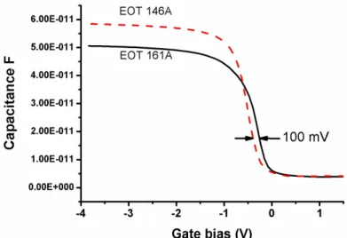
Finally the corresponding C-V characteristics were obtained from the samples to study the effect of the oxygen on the electrical properties of the silicided gate. The results reveal that the presence of unreacted oxygen-rich Si layer will increase
Fig. 6 Vfb versus EOT plots of devices with “localized FUSI” electrode.
The workfunction for the localized FUSI samples and control samples are 4.72eV and 4.63eV, respectively.
Fig. 5 Capacitance-Voltage curve of a MOS capacitor. Solid line is the capacitor fabricated by Ni reacting with furnace annealed Si. Dash line is the control sample. Equivalent oxide thickness (EOT) is calculated from Cox.
NiSi
NiSi
Si:O=96.7:3.3
SiO2
Si substrate
Fig. 4 XTEM of Ni silicide film formed by (a) annealed Si and (b) amorphous Si (the control sample). In (a), unreacted Si layer appears adjacent to the NiSi/SiO2 interface. EDS results show that about 3%
oxygen exists in this unreacted Si. In the control sample, fully silicidation is formed.
(a)
(b)
Si substrate
SiO2
equivalent oxide thickness as shown in Fig 5. The oxide
thickness calculated from the Cox of the control sample
correlated well with that of the elipsometer result, confirming the formation of FUSI gate. An approximate 100mV flat-band voltage shift was observed in the localized silicided sample as
compared to that of the control sample. A typical Vfb versus
EOT plot was used to extract the gate electrode workfunction as shown in Fig 6. The workfunction for the localized FUSI samples and control samples are 4.72eV and 4.63eV, respectively.
IV. Conclusion
In FUSI metal gate, impurities play a very important role in controlling the structural and electrical properties of the formed NiSi film. In this work, it was found that the presence of oxygen in the Si film will prevent effective Ni diffusion and retard FUSI formation during silicide process. These oxygen atoms will be
pushed down and pile up at the NiSi/SiO2 interface, and
eventually forms a layer of oxygen-rich unreacted Si adjacent to the interface. This unreacted Si layer will change the FUSI electrical properties, such as effective oxide thickness reduction, resulting in a flat-band voltage shift.
Acknowledgment
The authors would like to thank the Singapore-MIT Alliance, the National University of Singapore, the Nanyang Technological University and Institute of Materials Research & Engineering for supporting this work. Special thanks to Mr. Tung Chih-Hang for helping on X-TEM analysis.
References
[1] International Technology Roadmap for Semiconductors (ITRS) (SIA, San Jose, CA), http://www.itrs.net/Common/2004Update/2004Update.htm,
2004
[2] W. P. Maszara, “Fully silicided metal gates for high-performance CMOS technology: a review”, Journal of the Electrochemical Society, Vol. 152, 2005, pp. G550-G555 [3] Z. Krivokapic et al., “Nickel Silicide Metal Gete FDSOI
Devices with Improved Gate Oxide Leakage”, IEDM, 2002 [4] J.H. Sim et al., “Dual Work Function Metal Gates Using
Full Nickel Silicidation of Doped Poly-Si”, IEEE Electron Device Letters, Vol. 24, No. 10, Oct 2003, pp. 631- 633 [5] M. Qin, V. M. C. Poon, and S. C. H. Ho, J. “Investigation of
Polycrystalline Nickel Silicide Films as a Gate Material”, Journal of the Electrochemical Society, Vol. 148, May 2001, pp. 271-274
[6] J. H. Sim, H. C. Wen, J. P. Lu, and D. L. Kwong, “Dual work function metal gates using full nickel silicidation of doped poly-Si”, IEEE Electron Device Letters, Vol. 24, Issue 10, Oct 2003, pp. 631-633
[7] R. T. P. Lee, et al, “Fully silicided Ni1-xPtxSi metal gate
electrode for p-MOSFETs”, Electrochemical and Solid State Letters, Vol. 8, Issue 7, 2005, pp. G156-G159
[8] W. L. Tan and K. L. Pey, et al, “Effect of a titanium cap in reducing interfacial oxides in the formation of nickel silicide”, Journal of Applied Physics, Vol. 91, No. 5, Mar 2002, pp. 2901-2909
[9] J. Kedzierski, et al, “Threshold voltage control in NiSi-gated MOSFETs through silicidation induced impurity segregation (SIIS)”, IEDM Tech. Dig., 2003, pp. 315-318