HAL Id: hal-02892486
https://hal.archives-ouvertes.fr/hal-02892486
Submitted on 18 Sep 2020HAL is a multi-disciplinary open access archive for the deposit and dissemination of sci-entific research documents, whether they are pub-lished or not. The documents may come from teaching and research institutions in France or abroad, or from public or private research centers.
L’archive ouverte pluridisciplinaire HAL, est destinée au dépôt et à la diffusion de documents scientifiques de niveau recherche, publiés ou non, émanant des établissements d’enseignement et de recherche français ou étrangers, des laboratoires publics ou privés.
Electrically micro-polarized amorphous sodo-niobate
film competing with crystalline lithium niobate
second-order optical response
Lara Karam, Frederic Adamietz, Dominique Michaud, Claudia Gonçalves,
Myungkoo Kang, Rashi Sharma, Ganapathy Murugan, Thierry Cardinal,
Evelyne Fargin, Vincent Rodriguez, et al.
To cite this version:
Lara Karam, Frederic Adamietz, Dominique Michaud, Claudia Gonçalves, Myungkoo Kang, et al.. Electrically micro-polarized amorphous sodo-niobate film competing with crystalline lithium niobate second-order optical response. Advanced Optical Materials, Wiley, 2020, 8 (13), 2000202 (6 p.). �10.1002/adom.202000202�. �hal-02892486�
1
Electrically micro-polarized amorphous sodo-niobate film competing with crystalline
1
lithium niobate second order optical response
2 3
Lara Karam, Frédéric Adamietz, Dominique Michau, Claudia Gonçalves, Myungkoo Kang,
4
Rashi Sharma, G. Senthil Murugan, Thierry Cardinal, Evelyn Fargin, Vincent Rodriguez,
5
Kathleen A. Richardson, Marc Dussauze*
6 7
L. Karam, F. Adamietz, Prof. V. Rodriguez, Dr. M. Dussauze
8
Institut des Sciences Moléculaires, UMR 5255 CNRS
9
Université de Bordeaux
10
351 Cours de la Libération, 33405,Talence Cedex, France
11
E-mail : marc.dussauze@u-bordeaux.fr
12 13
D. Michau, Dr. T. Cardial, Prof. E. Fargin 14
Institut de Chimie de la Matière Condensée de Bordeaux, UMR 5026 CNRS
15
Universitéde Bordeaux
16
87 avenue du Dr. AlbertSchweitzer, 33600 Pessac Cedex, France
17 18
Dr. C. Gonçalves, Dr. M. Kang, Dr. R. Sharma, Prof. K. A. Richardson
19
CREOL, College of Optics and Photonics, Department of Materials Science and Engineering 20
University of Central Florida 21
Orlando, FL 32816, United States 22
23
Dr. G. S. Murugan 24
Optoelectronics Research Centre
25
University of Southampton
26
Southampton SO17 1BJ, United Kingdom
27 28
Keywords: nonlinear optical materials, amorphous thin films, poling 29
30
The design of active optical devices integrating second-order nonlinear (SONL) optical 31
responses typically relies on the use of dielectric crystalline materials such as lithium niobate 32
(LN)or semi-conductors such as GaAs. Despite high SONL susceptibilities, these materials 33
present important geometry constrains inherent to their crystalline nature limiting the 34
complexity of the designed photonic systems. Conversely, amorphous materials are versatile 35
optical media compatible with broad platform designs possessing a wide range of optical 36
properties attributable to their composition flexibility. Demonstrated here for the first time in 37
an amorphous inorganic material, we report a magnitude of SONL optical susceptibility((2)
38
=29 pm/V at 1.06 µm) comparable to that of LN single crystal. By using a thermo-electrical 39
imprinting process, fine control of the induced uniaxial anisotropy is demonstrated at the 40
micrometer scale. This work paves the way for the future design of integrated nonlinear 41
2
photonic circuits based on amorphous inorganic materials enabled by the spatially selective 42
and high SONL optical susceptibility of these promising and novel optical materials. 43
44 45
Research efforts towards the realization of efficient integrated photonic circuits (IPCs) where 46
active and passive optical components are combined on a single chip, have expanded over the 47
past decade. While this technology continues to mature, there remains significant challenges 48
associated with planar material optical function and multi-material integration. The design of 49
complex photonic structures requires a spatial control at widely varying length scales (from 50
micrometer to centimeter) and the merging of multiple optical and chemical functionalities 51
(for sensing devices). A promising platform for IPCs is silicon based[1] due to the very high 52
refractive index (RI) difference between the silicon waveguide and its cladding (air or silicon 53
oxide) which induces strong confinement of light allowing unprecedented small bend radii 54
(down to 1 µm); such attributes can thus minimize the resulting component’s footprint. 55
Thanks to this confinement, efficient third order optical processes like stimulated Raman 56
scattering have been observed in silicon waveguides[1]. However, as many active optical 57
devices rely on second order nonlinear (SONL) optical processes rather than third, silicon 58
cannot meet this demand as it is centrosymmetric and thus possesses a (2) of zero. Efforts to
59
modify this intrinsic behavior have been reported showing that one can break silicon’s 60
centrosymmetry and induce a (2) as high as 15 pm/V in a straight waveguide by depositing a 61
straining layer on the waveguide’s surface.[2] Another important platform for IPCs is lithium
62
niobate (LN).[3] LN exhibits good optical transparency spanning from the visible to mid-63
infrared as well as a strong SONL response ((2)zzz=55 pm/V for the single crystal grown from
64
the congruent melt)[4] making it a material of choice for active optical devices for 65
telecommunication. Traditional approaches to form waveguides in bulk LN through processes 66
3
like Ti+ diffusion have been shown to result in low RI differences and thus don’t allow for 67
complex structures. Unlike silicon, LN crystal is not isotropic thus enabling a strong SONL 68
optical response yet creating possible geometry restrictions in the realization of certain 69
devices. Several methods can be used to circumvent this problem. One is to use LN thin films 70
on insulators (LNOI) making possible the design of ridge and wire waveguides exhibiting 71
appreciable RI difference.[3] Quasi-phase matching (QPM) for frequency conversion has been 72
achieved on periodically grooved[5] dry etched or periodically poled[6] (based on domain 73
inversion) LNOI waveguides with good results. Another strategy employed is to use the LN 74
platform for its SONL optical properties but to rely on an easily patterned material to form the 75
guiding structure. Amorphous materials are good candidates for this task. Electro-optical 76
microring resonators and Mach-Zehnder interferometers have been realized on a LNOI 77
platform with a patterned chalcogenide thin film waveguide.[7] Compared to their crystalline 78
counterparts, amorphous materials are more flexible and versatile as they are compatible with 79
a range of forming processes and their optical properties can be tailored by tuning their 80
composition. 81
Since many active optical devices rely on SONL properties and since glass is isotropic, its use 82
is often limited to passive components such as waveguides. It is well known that breaking the 83
centrosymmetry of glass by heating the sample under a strong voltage followed by cooling 84
back down before removal of the DC field (or thermal poling) can result in the formation of a 85
stable SONL optical susceptibility at the glass’ surface. This process was first observed in 86
fused silica[8] and has since been extended to many different glass families including 87
silicate,[9] heavy metal oxides,[10–12] chalcogenides[13] among others. It can also be applied to 88
chromophores containing polymer[14–16]; hence, this constitutes a field of research beyond the 89
scope of this paper but such applicability to multiple systems highlights the versatility of the 90
approach. Thermal poling used as an imprinting process (employing a patterned electrode) has 91
resulted in the demonstration of rigorous spatial control of a stable SONL susceptibility at the 92
4
micrometer scale in different bulk glasses.[17,18] To date, limited efforts to extend this effect to 93
amorphous thin films suitable for integrated planar structures have been shown.[19–21] While 94
interesting findings have resulted from these studies, no amorphous inorganic material (in 95
bulk or thin film form) has to date exhibited SONL susceptibility levels of sufficient 96
magnitude to replace LN-based structures. 97
This work describes the patterning of SONL susceptibility of amorphous thin film in the 98
binary system Nb2O5-Na2O, demonstrating its potential as a promising candidate system with
99
a range of physical and optical properties suited to IPCs. To the best of our knowledge, only 100
one other group has reported the RF sputtering synthesis of amorphous NaNbO3 thin films.[22]
101
Here, we focus on one thin film composition containing 10 at.% of sodium with films 102
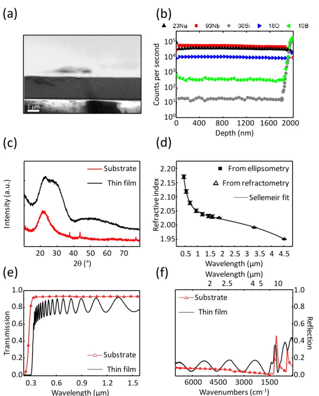
prepared by radiofrequency (RF) sputtering. The cross section of these films as investigated 103
by scanning electron microscopy (SEM) (Figure 1a) shows excellent thickness uniformity, 104
good adhesion to the borosilicate microscope slide substrate with no evidence of 105
delamination. The film appears homogenous at this scale, with no sign of porosity nor other 106
microstructural defects which could lead to light scattering. The composition homogeneity 107
throughout the thickness of the film has been confirmed by secondary ion mass spectroscopy 108
(SIMS) measurements (Figure 1b) and the film’s amorphous nature is validated by the x-ray 109
diffraction (XRD) diffractogram (Figure 1c). The optical properties of the film are shown 110
Figure 1d through 1f. The film’s refractive index dispersion has been quantified by two
111
different techniques (ellipsometry and refractometry) and measurements from both are in 112
good agreement; these data were successfully fitted using a Sellmeier equation[23] across a 113
large spectral window (0.5 to 4.5 µm) where the film is transmissive. The film exhibits a 114
refractive index of 2.046±0.005 at 1.064 µm which is comparable to that reported for 115
amorphous Nb2O5.[24] The transparency domain, reconstructed from transmission
116
measurements in the visible and reflection measurements in the infrared due to the substrate’s 117
absorption (Figure 1e and 1f), spans from 0.4 to 5 µm exhibiting comparable optical 118
5
transparency to that shown by LN.[3] These measurements also confirm the absence of light 119
scattering in the whole spectral region investigated, consistent with no evidence of 120
nanocrystallinity in the film. 121
An efficient thermo-electrical imprinting process on ionic bulk glasses is characterized by a 122
depletion of mobile cations under the conductive parts of the electrode. The next two figures 123
clearly illustrate how this process is successfully transferred to amorphous thin films in the 124
present work. The principle of the micro-poling treatment is illustrated in Figure 2a. Here, the 125
electrode is comprised of an indium tin oxide (ITO) thin film that is ablated by laser 126
irradiation to form alternating patterned regions of conductive and nonconductive zones. In a 127
manner similar to that used in previous studies on bulk glasses,[17] Raman mapping (Figure 128
2b through 2d) of the band centered at 850 cm-1 (Figure 2c) was used to track the sodium 129
distribution on the surface of the patterned film. This band is attributed to Nb-O stretching 130
modes where the oxygen is involved in an ionic bond with sodium. We observe a decrease of 131
this band for regions of the thin film under the conductive zones of the electrode (zone 2) 132
confirming the departure of sodium with the electrical field. Furthermore, a concurrent 133
evolution of the signature associated with molecular oxygen (mapping of the band at 134
1550 cm-1, Figure 2d) is seen, as observed in prior efforts where it was shown that this band is 135
associated with an electronic or anionic conduction that compensates for the departure of 136
positive charges.[25,26] Both maps show evidence of homogenous structural rearrangement of
137
the film, corresponding to the regions of the electrode’s pattern correlating and illustrating the 138
spatial precision of the imprinting process. The localization, the geometry and the magnitude 139
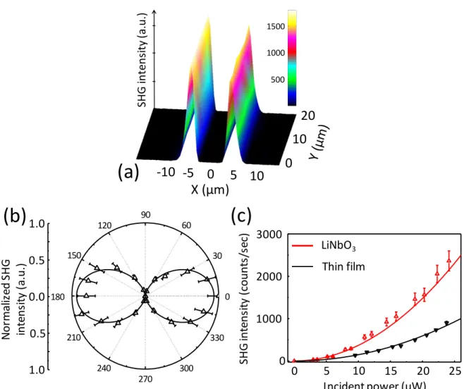
of the SONL optical response are discussed in Figure 3. Here, the second harmonic 140
generation (SHG), evidence of the SONL optical response in the film, was probed under 141
specular reflection conditions using a confocal microscope. The sample is oriented so that the 142
linearly polarized incident light is perpendicular to the imprinted line (along the X axis, see 143
Figure 2a for the orientation of the sample). The SHG signal is analyzed along the same 144
6
polarization orientation thus the term (2)xxx of the SONL susceptibility tensor is probed. The
145
SHG response is confined (c.f. Figure 3a) to regions where the sodium concentration gradient 146
is the strongest (i.e. at the edge of the conductive part of the electrode). It is maximal at the 147
border of the sodium-rich/sodium-depleted zones and decreases by three orders of magnitude 148
over less than three microns. 149
The SHG response in the patterned domains is largest when the sample is oriented as 150
described above (corresponding to 0 or 180° positions on the polar plot Figure 3b). When the 151
orientation of the sample turns the signal gradually decays following a square cosine function 152
to reach a complete extinction when the imprinted line is parallel to the incident light 153
polarization (corresponding to 90 or 270 ° on the polar plot). This directional variation shows 154
the uniaxial geometry of this response and the rigorous geometry control of the SONL 155
susceptibility. 156
In order to quantify the magnitude of the SONL optical susceptibility obtained using our 157
imprinting process on these sodo-niobate amorphous films, we have measured the SHG as a 158
function of the incident power and compared it to that of a reference (Figure 3c). The 159
reference material used is a bulk lithium niobate single crystal grown from a congruent melt. 160
Both measurements were made under the exact same experimental conditions. Here, the 161
incident and analyzed polarizations were along the bulk single crystal’s c-axis so that only the 162
strongest coefficient of the SONL susceptibility tensor of the crystalline reference 163
((2)zzz=55±6 pm/V)[4] was probed. The SHG signal’s quadratic dependence were fitted on the
164
basis of the classical theoretical expression of the SHG intensity as a function of the incident 165
power.[27] From these data, we extracted the magnitude of the thin film’s SONL susceptibility 166
using the ratio between the two quadratic law fitting coefficients, taking into account the 167
different refractive indices, and incorporating a correction for the surface’s reflection losses 168
(all details are given in the supporting information). Employing this protocol, the SONL 169
susceptibility micro-localized at the sodium-rich/sodium-depleted (on a scale of 3 µm) 170
7
frontier of these amorphous sodo-niobate films was determined to be 29±4 pm/V. After 171
demonstrating such accurate and spatially precise control of the second order optical 172
properties for these electrically polarized amorphous optical thin films, the next step is 173
naturally to progress toward the fabrication of features such as nonlinear optical amorphous 174
waveguides which would be important geometries in the design of a planar optical devices. 175
The lines that we have imprinted on the films are 5 mm long and a similar SHG response has 176
been measured over their whole length (±10 % in intensity). Hence, we can reasonably 177
prospect to apply this technique to induce a second order optical susceptibility over long 178
distances which could be of interest for the design of an electro-optical waveguide. To 179
achieve quasi phase patching conditions (QPM), a waveguide could be poled with a comb-180
like electrode (similar to the one used here[28]) on its side to obtain periodically alternating 181
SONL active and non-active domains. Now, if a similar comb-like electrode were to be put on 182
the other side of the waveguide but with a spatial offset, inverted domains could be formed 183
along the waveguide. According to the index dispersion of these niobate amorphous films 184
(Figure 1), the coherence length varies from 9 to 25 µm for wavelengths ranging from 1.5 to 3 185
µm; hence, the accuracy of the imprinting process demonstrated in this study denotes the 186
feasibility to pattern the SONL properties of these niobate amorphous materials within this 187
scale range. 188
In conclusion, we have synthesized and characterized the properties of amorphous sodo-189
niobate thin film materials. A thermo-electrical imprinting process was applied to these high 190
optical quality thin films extending to thin films previously observed in bulk poling 191
mechanisms. An unprecedented high SONL optical susceptibility for an amorphous inorganic 192
material, on the order of magnitude of that of crystalline LN was demonstrated and quantified 193
in side-by-side evaluation of both materials The fine control of the localization and the 194
geometry of the resulting SONL response enabled through the use of patterned electrode, has 195
demonstrated the potential viability of these materials in future devices. The fabrication 196
8
flexibility guaranteed by the amorphous nature of the sodo-niobate thin film combined with 197
an easy protocol to induce microscale, local uniaxial anisotropies with (2) values, competing 198
with a crystalline LN, opens vast new opportunities for the design and manufacturing of 199
planar photonic architectures for the visible through mid-infrared spectral region. 200
201
Experimental Section
202
Detailed experimental procedures are reported in the Supporting Information. 203
204
Supporting Information
205
Supporting information is available from Wiley Online Library or from the author. 206
207
Acknowledgments
208
The authors would like to thank Mikhail Klimov, at the Material Characterization Facility 209
(MCF) at UCF for conducting the SIMS measurements and Pieter Kik (CREOL) for giving 210
access to his ellipsometer, Eric Lebraud, at the ICMCB common characterization service for 211
carrying the XRD measurements. The authors also appreciate the helpful discussions with 212
Juejun Hu at MIT for his relevant suggestions related to photonic device design constraints 213
and requirements. The authors gratefully acknowledge the financial support of: IdEx 214
Bordeaux (Cluster of Excellence LAPHIA and the allocated grant referred to as ANR-10-215
IDEX-03-03), the IdEx Bordeaux Visiting Scholar program, and the CNRS project 216
EMERGENCE @INC2019. This project has received funding from the European Union’s 217
Horizon 202 research program under the Marie Skłodowska-Curie grant agreement No 218
823941 (FUNGLASS). 219
220
Competing Interests statements:
221
The authors declare no competing interests. 222 223 224 Received: 225 Revised: 226 Published online: 227 228 References 229
[1] W. Bogaerts, P. De Heyn, T. Van Vaerenbergh, K. De Vos, S. Kumar Selvaraja, T. 230
Claes, P. Dumon, P. Bienstman, D. Van Thourhout, R. Baets, Laser & Photon. Rev. 231
2012, 6, 47.
232
[2] R. S. Jacobsen, K. N. Andersen, P. I. Borel, J. Fage-Pedersen, L. H. Frandsen, O. 233
Hansen, M. Kristensen, A. V. Lavrinenko, G. Moulin, H. Ou, C. Peucheret, B. Zsigri, A. 234
Bjarklev, Nature 2006, 441, 199. 235
9
[3] A. Boes, B. Corcoran, L. Chang, J. Bowers, A. Mitchell, Laser & Photonics Reviews 236
2018, 12, 1700256.
237
[4] V. G. Dmitriev, G. G. Gurzadyan, D. N. Nikogosyan, Handbook of Nonlinear Optical 238
Crystals, Springer Berlin Heidelberg, Berlin, Heidelberg, 1997.
239
[5] C. Wang, X. Xiong, N. Andrade, V. Venkataraman, X.-F. Ren, G.-C. Guo, M. Lončar, 240
Opt. Express 2017, 25, 6963.
241
[6] L. Chang, Y. Li, N. Volet, L. Wang, J. Peters, J. E. Bowers, Optica 2016, 3, 531. 242
[7] A. Rao, A. Patil, J. Chiles, M. Malinowski, S. Novak, K. Richardson, P. Rabiei, S. 243
Fathpour, Opt. Express 2015, 23, 22746. 244
[8] R. A. Myers, N. Mukherjee, S. R. Brueck, Optics Letters 1991, 16, 1732. 245
[9] F. C. Garcia, I. C. S. Carvalho, E. Hering, W. Margulis, B. Lesche, Applied Physics 246
Letters 1998, 72, 3252.
247
[10] B. Ferreira, E. Fargin, B. Guillaume, G. Le Flem, V. Rodriguez, M. Couzi, T. Buffeteau, 248
L. Canioni, L. Sarger, G. Martinelli, Y. Quiquempois, H. Zeghlache, L. Carpentier, 249
Journal of Non-Crystalline Solids 2003, 332, 207.
250
[11] K. Tanaka, A. Narazaki, K. Hirao, Opt. Lett. 2000, 25, 251. 251
[12] V. Nazabal, E. Fargin, J. J. Videau, G. Le Flem, A. Le Calvez, S. Montant, E. Freysz, A. 252
Ducasse, M. Couzi, Journal of Solid State Chemistry 1997, 133, 529. 253
[13] M. Guignard, V. Nazabal, F. Smektala, J.-L. Adam, O. Bohnke, C. Duverger, A. 254
Moréac, H. Zeghlache, A. Kudlinski, G. Martinelli, Y. Quiquempois, Adv. Funct. Mater. 255
2007, 17, 3284.
256
[14] S. K. Yesodha, C. K. Sadashiva Pillai, N. Tsutsumi, Progress in Polymer Science 2004, 257
29, 45.
258
[15] L. Dalton, in Polymers for Photonics Applications I (Ed.: K.-S. Lee), Springer Berlin 259
Heidelberg, Berlin, Heidelberg, 2002, pp. 1–86. 260
10
[16] P. Labbé, A. Donval, R. Hierle, E. Toussaere, J. Zyss, Comptes Rendus Physique 2002, 261
3, 543.
262
[17] M. Dussauze, V. Rodriguez, F. Adamietz, G. Yang, F. Bondu, A. Lepicard, M. Chafer, 263
T. Cardinal, E. Fargin, Advanced Optical Materials 2016, 4, 929. 264
[18] A. Lepicard, F. Adamietz, V. Rodriguez, K. Richardson, M. Dussauze, Opt. Mater. 265
Express 2018, 8, 1613.
266
[19] Y. Quiquempois, A. Villeneuve, D. Dam, K. Turcotte, J. Maier, G. Stegeman, S. 267
Lacroix, Electronics Letters 2000, 36, 733. 268
[20] M. Dussauze, A. Malakho, E. Fargin, J. P. Manaud, V. Rodriguez, F. Adamietz, B. 269
Lazoryak, Journal of Applied Physics 2006, 100, 013108. 270
[21] A. S. K. Tong, F. Bondu, G. Senthil Murugan, J. S. Wilkinson, M. Dussauze, Journal of 271
Applied Physics 2019, 125, 015104.
272
[22] V. Lingwal, N. S. Panwar, Journal of Applied Physics 2003, 94, 4571. 273
[23] J. D. Musgraves, J. Hu, L. Calvez, Springer Handbook of Glass, 2019. 274
[24] Ö. D. Coşkun, S. Demirel, G. Atak, Journal of Alloys and Compounds 2015, 648, 994. 275
[25] T. Cremoux, M. Dussauze, E. Fargin, T. Cardinal, D. Talaga, F. Adamietz, V. 276
Rodriguez, The Journal of Physical Chemistry C 2014, 118, 3716. 277
[26] M. Dussauze, V. Rodriguez, A. Lipovskii, M. Petrov, C. Smith, K. Richardson, T. 278
Cardinal, E. Fargin, E. I. Kamitsos, J. Phys. Chem. C 2010, 114, 12754. 279
[27] R. W. Boyd, Nonlinear Optics, Elsevier, 2003. 280
[28] P. Mackwitz, M. Rüsing, G. Berth, A. Widhalm, K. Müller, A. Zrenner, Appl. Phys. Lett. 281
2016, 108, 152902.
282
[29] N. Bloembergen, P. S. Pershan, Phys. Rev. 1962, 128, 606. 283
11 284
Figure 1. Characterization of the sodo-niobate film: a) Thin film on glass slide cross section
285
viewed by SEM, the scale bar is 1 µm. b) SIMS profile recorded through the depth of the 286
film. Silicon and Boron concentration increase shows that the borosilicate glass substrate 287
interface was reached. c) XRD pattern of the bare borosilicate substrate (in red) and that of the 288
thin film (black) confirming the amorphous nature of both; the three peaks on the substrate’s 289
diffractogram originate from the sample holder (aluminum). d) Film refractive index 290
dispersion obtained by a Sellmeier fit on data extracted from two different techniques; on the 291
refractometry measurements (opened squares) the error is within the size of the data point. 292
The transparency window of a 1.4 µm thick film in black: transmission in the visible (e) and 293
reflection in the infra-red (f); as a comparison the substrate’s spectra are also presented in red 294 (opened triangles). 295 296 20 30 40 50 60 70 2q(°) Int ens it y (a .u .) Substrate Thin film 0 400 800 1200 1600 2000 Depth (nm) 100 101 103 102 104 105 C ount s pe r se co nd 0.5 1 1.5 2 2.5 3 3.5 4 4.5 Wavelength (µm) 2.20 2.15 2.10 2.05 2.00 1.95 R ef ra ct iv e inde x 1.0 0.8 0.6 0.4 0.2 0.0 Tr ans m is si on 0.3 0.6 0.9 1.2 1.5 Wavelength (µm) 6000 4500 3000 1500 Wavenumbers (cm-1) 1.0 0.8 0.6 0.4 0.2 0.0 R ef le ct ion 2 2.5 4 5 10 Wavelength (µm)
(c)
(d)
(e)
(b)
(a)
(f)
Substrate Thin film Substrate Thin film From ellipsometry From refractometry Sellemeir fit 1 µm
12 297
Figure 2. Thermo-electrical micro-imprinting process: a) Schematic of the process: the
sodo-298
niobate thin film is deposited on a borosilicate glass slide (1), and heated while a strong 299
voltage is applied by a structured electrode (in contact with the sample as opposed to some 300
other techniques)[5] (2) and cooled back down before turning the DC field off. This gives rise 301
to two different zones on the post-processed sample (3). b) (top) The characteristic Raman 302
spectra (top) extracted from zone 1 (red) and 2 (black). The spectra have been normalized by 303
the area under the curve. To illustrate evidence of the structural variations of the two regions, 304
the difference Raman spectra is presented (bottom), corresponding to the response in zone 1 305
(unaffected by poling) subtracted to the poled region in zone 2. c), d) Spatial evolution of two 306
different bands: (c) corresponds Nb-O stretching modes associated with Nb-O-…Na+
307
structural units, and (d) to spectral region illustrating the presence of molecular oxygen 308
attributed to compensation mechanisms occurring during poling.[17] 309 0 5 10 -10 -5 0 5 10 15 (µm) (µ m ) 0.015 0.010 0.005 0.000 0 5 10 -10 -5 0 5 10 15 (µm) (µ m ) 0.01 0.00 -0.01 -0.02 ¤
2
1
3
N or m al iz ed R am an int ens it y (a .u .) R am an di ff er ence (a .u .) 0.6 0.4 0.2 0.0 -0.1 0.1 400 800 1200 1600 Wavenumbers (cm-1) Zone 1 Zone 2(b)
(c)
(a)
Zone 1 Zone 2¤
(2)
(1)
(3)
X
X
Y
Y
(d)
13 310
Figure 3. Localization, geometry and magnitude of the induced SONL optical response. a)
311
SHG intensity map realized on the poled film with a linearly polarized light (VV) 312
perpendicular to the imprinted line. b) Normalized SHG intensity as a function of the 313
orientation of the sample (0-180 ° corresponds to the imprinted line perpendicular to the 314
incident light polarization and 90-270 ° parallel). The data were normalized to the maximum 315
value. Repeating the experiment several times allows estimation of error bars to a value of 316
approximately 15 %. A fit with a cos2 function demonstrates the uniaxial geometry of the
317
response. c) SHG intensity as a function of the linearly polarized incident light power for the 318
thin film (in black – oriented so that the imprinted line is perpendicular to the incident light) 319
and for the LN single crystal (in red – oriented so that the c axis is collinear to the incident 320
light polarization and so that (2)zzz is probed). The error bar was estimated by repeating the
321
measurements. The continuous lines correspond to quadratic fits. 322 323
0
5 10
-5
-10
X (µm)
0
10
20
SHG in ten si ty ( a.u .) 1500 1000 500(a)
5 10 15 20 25 Incident power (µW) 1000 2000 3000 0 SH G int ens it y (count s/ se c) LiNbO3 Thin film 1.0 0.5 0.0 0.5 1.0 N or m al iz ed S H G int ens it y (a .u .) 0 30 60 90 270 180 120 150 210 240 300 330(b)
(c)
0
14
A second order nonlinear optical susceptibility is induced by a thermo-electrical imprinting 324
treatment in an amorphous thin film. A magnitude for the (2) of 29 pm/V is measured, this 325
value is the highest ever reported for an amorphous inorganic material. The induced uniaxial 326
anisotropy is localized at the micrometer scale opening the way for new active planar 327
photonic architectures based on amorphous materials. 328
329
Nonlinear Optical Materials
330 331
Lara Karam, Frédéric Adamietz, Dominique Michau, Claudia Gonçalves, Myungkoo Kang, 332
Rashi Sharma, G. Senthil Murugan, Thierry Cardinal, Evelyn Fargin, Vincent Rodriguez, 333
Kathleen A. Richardson, Marc Dussauze* 334
335
Electrically micro-polarized amorphous sodo-niobate film competing with crystalline
336
lithium niobate second order optical response
337 338 339 340 LiNbO3 Thin film Incident Power SH G in te n si ty SH G in te n si ty Sample’s orientation 0 90 270 SH G in te n si ty