Plasma Science and Fusion Center Massachusetts Institute of Technology
Cambridge MA 02139 USA
This work was supported by the U.S. Department of Energy,
Grant No. DE-FC02-99ER54512. Reproduction, translation, publication, use and disposal, in whole or in part, by or for the United States government is permitted.
PSFC/RR-07-8 DOE/ET-54512-361
Construction and Operation of a
Mirror Langmuir Probe Diagnostic for the
Alcator C-Mod Tokamak
Construction and Operation of a Mirror Langmuir Probe
Diagnostic for the Alcator C-Mod Tokamak
by
Laurence Anthony Lyons
B.S., Electrical Engineering and Economics
Rensselaer Polytechnic Institute, 2005
Submitted to the Department of Electrical Engineering and Computer Science in Partial Fulfillment of the Requirements for the Degree of
Master of Science in Electrical Engineering and Computer Science at the MASSACHUSETTS INSTITUTE OF TECHNOLOGY
May 18, 2007
©2007 Massachusetts Institute of Technology All Rights Reserved.
Author__________________________________________________________________
Department of Electrical Engineering and Computer Science May 18, 2007
Certified by _____________________________________________________________
Dr. Brian LaBombard Principal Research Scientist, Alcator Project, MIT Plasma Science and Fusion Center Thesis Supervisor
Certified by _____________________________________________________________
Dr. Ronald R. Parker Professor of Nuclear Engineering, and Electrical Engineering and Computer Science Thesis Supervisor
Accepted by_____________________________________________________________
Arthur C. Smith Chairman, Department Committee on Graduate Studies Electrical Engineering and Computer Science
Construction and Operation of a Mirror Langmuir Probe Diagnostic for the Alcator C-Mod Tokamak
by
Laurence Anthony Lyons Submitted to the
Department of Electrical Engineering and Computer Science May 18, 2007
In Partial Fulfillment of the Requirements for the Degree of Master of Science in Electrical Engineering and Computer Science
ABSTRACT
Langmuir probe diagnostic systems presently employed on Alcator C-Mod and elsewhere generally suffer from a severe limitation: unless multiple electrode or high-frequency bias techniques are employed, these systems can not resolve the rapid changes in plasma electron temperature, floating potential and ion saturation current that are associated with plasma turbulence. Moreover, no existing system can provide real-time output of these three parameters using a single electrode. To remedy this limitation, an advanced, high-bandwidth Langmuir probe system has been constructed for Alcator C-Mod using state-of-the-art design tools and components. The system produces a fast-switched, three-state probe bias waveform and employs a new method for outputting plasma conditions in real-time, a ‘Mirror Langmuir Probe’ (MLP), which utilizes high-bandwidth bipolar transistors to electrically simulate a Langmuir probe’s response. Detailed information on the design, construction and performance of this new diagnostic is described in this thesis, representing the first proof-of-principle demonstration of the MLP technique. The MLP system was found to meet all the performance goals set forth at the beginning of the project: real-time output of electron temperature, floating potential and ion saturation current, ability to track changes in plasma parameters within a ~1 μs timescale, while utilizing only a single Langmuir electrode. The system was tested using an ‘electronic Langmuir probe’ and also using an actual Langmuir probe in Alcator C-Mod. In both cases, the system accurately locked onto changing plasma conditions (< ~5% error in outputted parameters), with the exception of some severe transient events found in C-Mod plasmas (ELMs), which challenged the system’s accuracy. Further refinements to the system have been identified to handle such cases. The MLP clearly demonstrated superior performance to existing Langmuir probe systems on Alcator C-Mod and should enable researchers to study edge plasma turbulence in much greater detail in the future.
Thesis Supervisor: Dr. Brian LaBombard
Title: Principal Research Scientist, Alcator Project, MIT Plasma Science and Fusion Center Thesis Supervisor: Dr. Ronald Parker
Acknowledgements
Several members of the MIT Plasma Science and Fusion Center (PSFC) contributed substantially to the work found in this thesis and I would like to recognize them here. First on that list is Dr. Brian LaBombard who first brought me onto this project as a summer intern four years ago. If he wasn’t willing to take a chance on a inexperienced sophomore from RPI, then this thesis would have never existed. Furthermore, Brian’s support, constant feedback and desire to find an optimal solution to every problem enabled this complex project to reach successful completion. This thesis represents the largest achievement of my life and it would not have been possible without Brian.
I would also like to mention William Burke and Bill Parkin from the PSFC who were instrumental in teaching me how to use the latest circuit design and simulation software. Although both have busy schedules, they were always willing to take the time to help me through a problem or explain certain techniques. Without these two, learning how to design circuits would have been much more complicated.
Finally, I would like to recognize the PSFC electronics shop and in particular Wade Cook and Dave Bellofatto. In a lab full of expensive equipment, both Wade and Dave gave me full accesses to anything that I needed and always took the time to teach me how to use new equipment. I learned everything I know about constructing circuit boards from these two and would like to thank them for their help.
Table of Contents
List of Figures
... 9Chapter 1 – Introduction
... 111.1 – Background and Motivation ... 11
1.2 – Goals and Outline of Thesis... 13
Chapter 2 – Langmuir Probes
... 152.1 – Plasma Basics... 15
2.2 – An Electric Probe in a Plasma ... 16
2.3 – Langmuir Probe Methods ... 21
Chapter 3 – Mirror Langmuir Probe Theory
... 253.1 – Goals of New Langmuir Probe System ... 25
3.2 – Fundamental Theory of Mirror Langmuir Probe ... 25
3.3 –Mirror Langmuir Probe System Concept... 28
Chapter 4 – Mirror Langmuir Probe System Design
... 314.1. - System Overview... 31
4.2 - TTL Waveform Generator... 36
4.3 - FET Drive Board ... 44
4.4 – MLP Data Board... 60
Chapter 5 – MLP System Bench Performance Tests
... 835.1 – Electronic Langmuir Probe Overview ... 83
5.2 – MLP Performance Test – Static Parameters on ELP ... 87
5.3 – MLP Performance Test – Variable Parameters on ELP ... 92
Chapter 6 – MLP System Tests – Real Plasma
... 996.1 – Experimental Set-up... 99
6.2 – Initial MLP Data from Real Plasma... 100
6.3 – Capacitive Coupling and Bias Range Checks... 101
6.4 – Comparison of Real-Time Output with Post-Processing Analysis... 102
Chapter 7 – Summary and Conclusion
... 117Bibliography
... 119Appendix A – Mirror Langmuir Probe Circuit Schematics
... 121TTL Waveform Generator Circuit ... 121
FET Drive Circuit ... 122
MLP Data Circuit... 123
Appendix B – Post Processing Methods to Compute Te, Vf, and Isat from
Langmuir Probe Current and Voltage Data
... 125Method 1 ... 125
List of Figures
Figure 2.1 - Example of the Electric Potential Variation near the Surface of Probe [3] ... 17
Figure 2.2 – Example of a Langmuir Probe I-V Characteristic [3] ... 20
Figure 3.1 – Bipolar Transistor Pair Biased to Mimic Langmuir Probe Response [9]... 26
Figure 3.2 – MLP System Concept [9] ... 29
Figure 4.1 – MLP System Block Diagram... 32
Figure 4.2 – MLP Rack Assembly... 33
Figure 4.3 – TTL Waveform Generator Functional Block Diagram ... 36
Figure 4.4 – Trigger and Time Duration Limit Circuit... 37
Figure 4.5 – Internal and External Clock Circuit... 39
Figure 4.6 – Waveform Generator Circuit... 40
Figure 4.7 – Power Indicator Circuit ... 41
Figure 4.8 – TTL Waveform Generator Layout ... 42
Figure 4.9 – TTL Waveform Generator Signal Output ... 43
Figure 4.10 – FET Drive Functional Block Diagram ... 45
Figure 4.11 – FET Switching Output Circuit... 46
Figure 4.12 – Probe Bias Regulator Circuit... 49
Figure 4.13 – Isat Level Monitor Circuit... 51
Figure 4.14 – Variable Coupling Capacitances Circuit ... 51
Figure 4.15 – FET Board with Shield and MLP Data Board Interconnections... 53
Figure 4.16 – FET Board without Shield... 54
Figure 4.17 – FET Board Output (Max Bias) with TTL Signals... 56
Figure 4.18 – FET Board Output (Min Bias) with TTL Signals ... 57
Figure 4.19 – FET Board Output with Variable Bias ... 58
Figure 4.20 – FET Board Output with Rapidly Changing Isat ... 59
Figure 4.21 – Slow Changing Isat with Capacitance Effects on Waveform ... 60
Figure 4.22 – MLP Data Circuit Functional Block Diagram... 61
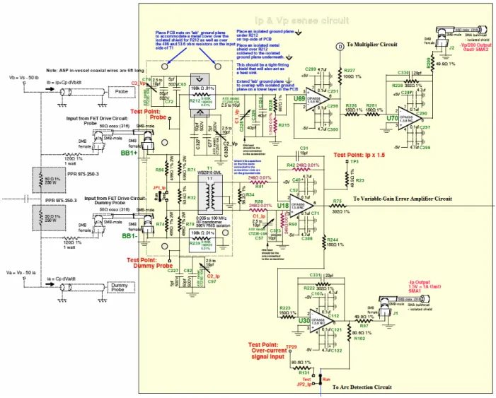
Figure 4.23 – Current and Voltage Sense Circuit... 62
Figure 4.24 – Method to Compensate for Parasitic Capacitance R212 ... 64
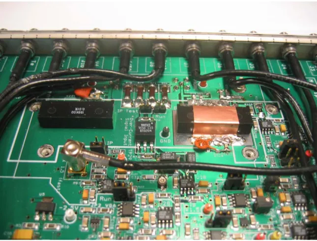
Figure 4.25 – Current and Voltage Sense Circuit Photo... 65
Figure 4.26 – Multiplier Circuit... 67
Figure 4.27 – Mirror Langmuir Probe Circuit ... 68
Figure 4.28 – Variable-Gain Error Amplifier Circuit... 72
Figure 4.29 – Isat Error-Integrator Circuit... 73
Figure 4.30 – Vf Error-Integrator Circuit ... 75
Figure 4.31 – Te Error-Integrator Circuit ... 76
Figure 4.32 – Error-Signal Sample-and-Hold Circuits... 78
Figure 4.33 – FET Switch Drive Circuit... 79
Figure 4.34 – Probe Bias Amplitude Circuit ... 80
Figure 4.35 – MLP Data Board with Shield ... 81
Figure 5.1 – Various Adjustable Parameters on Electronic Langmuir Probe Circuit... 84
Figure 5.2 – Transistor Core of Electronic Langmuir Probe Circuit ... 86
Figure 5.3 – Static ELP Test – Long Time Scale ... 88
Figure 5.5 – Static ELP Test – Small Time Scale... 91
Figure 5.6 – Variable ELP Test ... 94
Figure 5.7 – Variable ELP Test – Small Time Scale with M2 Output ... 95
Figure 5.8 – Variable ELP Test – Smaller Time Scale with M2 Output ... 96
Figure 5.9 – Variable ELP Test – Small Time Scale with M1 Output ... 97
Figure 5.10 – Variable ELP Test – Small Time Scale with M1 Output ... 98
Figure 6.1 – Cross-section of Alcator C-Mod and Horizontal Probe Head Detail ... 104
Figure 6.2 – Global Plasma Parameters for Alcator C-Mod Shot 1070406029 ... 105
Figure 6.3 – MLP Data from Alcator C-Mod with Floating Probe Overlay ... 106
Figure 6.4 – MLP Data from Alcator C-Mod with Floating Probe Overlay ... 107
Figure 6.5 – MLP Data from Alcator C-Mod with Floating Probe Overlay ... 108
Figure 6.6 – MLP Data from Alcator C-Mod with Floating Probe Overlay ... 109
Figure 6.7 – MLP Data from Alcator C-Mod with Floating Probe Overlay ... 110
Figure 6.8 – MLP Data from Alcator C-Mod with Floating Probe, Vf and Isat Overlay... 111
Figure 6.9 – MLP Data from Alcator C-Mod with M2 Output Overlaid ... 112
Figure 6.10 – MLP Data from Alcator C-Mod with M2 Output Overlaid ... 113
Figure 6.11 – MLP Data from Alcator C-Mod with Computed Current and Error Signals ... 114
Chapter 1 – Introduction
1.1 – Background and Motivation
Langmuir probes are one of the oldest and most fundamental plasma diagnostics. Their usefulness is demonstrated by the wide range of plasmas in which they can be used to infer plasma parameters [1-3]. From low temperature plasmas (~0.05 to ~5eV) to those of moderate temperature (~5eV to ~100eV) and high electron density (~1020 m-3), a Langmuir probe can be used to measure local electron temperature, densities and electric potentials. Each of these parameters is obtained by applying a voltage (V) to a Langmuir probe and measuring the resultant current (I). From this I-V characteristic, parameters such as electron temperature, ion saturation current and floating potential can be deduced by fitting the data points with model parameters.
The most straightforward use of a Langmuir Probe involves only one electrode, which is inserted into the plasma region of interest and biased with respect to the metallic chamber that contains the plasma. The bias voltage is typically swept at a given frequency over a range that is comparable to the electron temperature. Transient analog-to-digital (A/D) recorders are typically used to record the Langmuir probe’s I-V characteristic for a given plasma discharge. Plasma parameters of interest are later extracted during a post-processing step, where customized software is used to fit the I-V characteristic.
At the MIT Plasma Science and Fusion center, the tokamak plasma confinement experiment Alcator C-Mod makes use of several Langmuir Probes (single electrode type) at various locations to make plasma edge measurements using the method described above. Although this system works well in an ideal world, two principle issues have limited the effectiveness of the measurements made with these probes. First, owing to bandwidth limitations of the bias and I-V sensing electronics, the voltage applied to the probe is swept at a frequency of 2 kHz or less. This is an issue because plasma turbulence can change the local values of electron temperature, ion saturation current and floating potential over a much shorter time scale, on the order of a microsecond [4]. On the current Alcator systems, the turbulent fluctuations show up as ‘noise’ on
the I-V characteristic. The fitted data is therefore useful to track long time-scale trends only. Moreover, parameters derived from a least-squares fit to such a ‘noisy’ I-V characteristic may be in error since the I-V response is actually a nonlinear function of plasma potential and electron temperature fluctuations.
The second limitation deals with the post-processing needed to extract the plasma parameters from the I-V data points. Since the data processing step is computationally intensive, it can not provide researchers with valuable real-time information. For example, if real time values for the parameters were available, they could be used in a feedback system to alter the voltage waveform being applied. This is advantageous because the voltage bias to a Langmuir probe has an optimal range for a given set of plasma parameters. On the current Alcator system, a best guess is made before hand on what the average plasma parameters will be and the bias is set accordingly.
The limitations of the current Langmuir probe system on Alcator C-Mod are significant enough to necessitate an upgrade. What kind of upgrade to apply is where this thesis project begins. Alternative schemes already exist that have advantages over the current C-Mod system. These include the triple probe method [5], which can directly output all three plasma parameters of interest and the double probe method [6] that can output electron temperature directly. One clear drawback of these systems is that they involve more than one probe which means the current mechanical systems on C-Mod would have to be changed to accept additional probes. The second problem with these systems is the assumption that plasma parameters are the same at each probe for a given measurement, which because of turbulence [7] would almost never be the case.
Recently, a new idea for a Langmuir probe bias scheme was proposed based on the concept of a ‘Mirror Langmuir Probe’ (MLP) [8, 9]. The MLP utilizes only one electrode and involves a new concept of linking the I-V characteristics found in the edge of a magnetically confined plasma with the I-V characteristic found in bipolar RF transistors. By constructing a system of active feedback around the transistors, one can imagine a system that forces the rf transistors to mimic the Langmuir probe’s I-V response in a scaled down manner. Once the I-V responses are
matched, the circuitry can output the plasma parameters in real-time. Furthermore, the entire system could utilize state-of-the-art components to ensure that the system will be fast enough to track the rapid (on the order of a microsecond) changes caused by the plasma turbulence.
The theoretical basis for the MLP has already been developed by Dr. Brian LaBombard of the MIT PSFC and was not the focus of this work. Instead, this thesis was concerned with the construction and operation of an actual MLP system. The scope of this thesis involved everything from initial proof-of-principle computer modeling through proto-board development of each subsystem to a final working version of the circuit boards that make up the MLP system.
1.2 – Goals and Outline of Thesis
The goal of this thesis was to build a working Mirror Langmuir Probe system for probes on Alcator C-Mod based on the concepts outlined by Dr. LaBombard. Chapter 2 covers the basics of Langmuir probes and demonstrates how the current systems in use today are not capable of resolving the effects of turbulence in magnetically confined fusion devices. An in-depth overview of Dr. LaBombard’s theory is covered in Chapter 3, which subsequently sets the framework for the majority of the work performed on this project. Chapter 4 shows the fruit of this labor and details the circuit boards that achieved the design parameters specified by the MLP theory. A custom-designed electronics package was assembled using state-of-the art components and designed with the help of the latest circuit construction, simulation and fabrication tools. The OrCAD suite [10] of electronic design and simulation software was used for this purpose. In particular, this effort focused on the design and fabrication of the key components: a master-clock timing module (TTL Waveform Board), a fast-switching probe voltage drive board using high-voltage RF MOSFETs (FET Driver Board), and an analog computer board, implementing the Mirror-Probe method to deduce plasma parameters in real-time (MLP Data Board). While the performance of these circuits is also covered in Chapter 4, the bench testing of the system as a whole is reserved for Chapter 5. Finally, Chapter 6 presents results from initial tests of the MLP system using Langmuir probes on Alcator C-Mod. A summary of this thesis project with suggestion for future work is contained in Chapter 7.
Chapter 2 – Langmuir Probes
(
Note: If the reader already possesses a basic knowledge of plasma physics and Langmuir probe theory, please skip to section 2.3 for a review of current probe techniques before moving onto Chapter 3)Before an in-depth description of the Mirror Langmuir Probe (MLP) concept can be covered, a basic understanding of plasma physics is required. In particular, the interaction of the charged particles in a fully ionized plasma with a solid object is crucial to understanding what a Langmuir probe is used for and how it works. Please note that the analysis provided below is highly simplified, but accurate enough to explain the basic forces at work. In certain situations, such as with a magnetized plasma, the true complexity of this interaction reaches depths that are still not fully understood or correctly modeled to this day [11, 12].
2.1 – Plasma Basics
Plasma, quite simply, is the fourth state of matter. Unlike the other three states which involve the chemical bonding between atoms or molecules, a plasma is created when electrons are able to overcome the electric forces binding them to their orbits. When this binding energy is overcome by an electron, it becomes disassociated with the nucleus and is able to move on its own. The remaining atom is left with a net positive charge, becoming an ion. So long as the electron remains energetic enough to overcome the electric force attracting it to the ion, these two particles will not recombine. When sufficient numbers of these free electrons and ions exist in a region of space, they are collectively called the plasma state of matter.
The two most common methods to create a plasma are by either heating a gas to a high temperature where the atomic collisions are so strong that electrons are “knocked loose” or by exposing a gas to a strong enough electric field that the electrons are pulled from the atoms they occupy. Initially, only one electron is removed from an atom when it is ionized as the positive charge created on the atom by the departure of the first electron causes the energy needed to
remove a second one to be much higher. Furthermore, more stable atoms such as those with filled valance bands (i.e. helium atoms) require more energy to ionize than atoms with unfilled bands (i.e. hydrogen atoms).
When a large number of particles are ionized, they form a sea of positive and negative charges that must coexist together. Although these particles are energetic enough to keep from recombining, the negative and positive charges still affect each other and can create electric fields if too much of one charge builds up in a certain area. Because of these interactions, the plasma cloud quickly reaches a steady state where the net charge of any section of the cloud is always near zero. Although the ions and electrons are moving around this cloud, a net charge will never develop as long as an external force or perturbation is not introduced. Furthermore, through collisions, the populations of electrons and ions tend towards having the same temperature. As a result, the electrons have a much high velocity than the comparably massive ions [3].
2.2 – An Electric Probe in a Plasma
One of the first methods developed to study plasma was to simply insert an object into it (usually a conductor) and study its effect on the plasma. Although any object will do, a metallic probe will be used for this example. When an electrically isolated probe is instantaneously introduced to the plasma, it is exposed to the free flowing electrons and ions. Due to the electron’s higher velocity, more electrons will initially strike the probe than ions, which causes a negative voltage to build on the probe in relation to the otherwise ambient potential of the plasma, ΦP [13].
Eventually, the probe will start to repel a certain percentage of electrons as it becomes biased further negative. Meanwhile, the heavier, slow-moving ions become attracted by the probe, but can only approach the probe at the maximum “plasma-fluid” velocity, i.e., the sound speed [3]. Thus, even though the probe is building up negative charge, the ion particle flux on the probe tends to remain the same1. For this reason, the rate of ion collection by the probe is called the
1 NOTE: For cylindrical or spherical probe geometries in a plasma without a magnetic field, the “ion saturation current” is more generally a function of Vb as the Debye shielding distance varies with bias. However, when a magnetic field is present, the motion of the ions is constrained to follow the field lines. In this case, the ion collection rate becomes independent of bias as long as the probe size is larger than the ion Larmor radius and the Debye length. The latter case is highlighted here.
“ion saturation current” (Isat). Finally, the bias on the probe (Vb) will reach a level, called the
floating potential (Vf), where the particle flux or current from the electrons (Ielec) has been
reduced enough by the negative bias to be equal to the current coming from the ions. Thus, in this “floating state” the following equations are satisfied:
f b V V = (2.1) electron sat
I
I
=
−
(2.2)0
=
=
electron+ sat probeI
I
I
(2.3)Figure 2.1 - Example of the Electric Potential Variation near the Surface of Probe [3]
Since this probe is now at a different potential level than the surrounding plasma, the previous unperturbed state of quasi-neutrality has been lost. The floating potential Vf is significantly
more negative than the plasma potential with a difference that is typically on the order of three times the electron temperature (Te) [14]. In order to maintain this state, the plasma creates a
buffer zone around the probe called the sheath. This sheath region is very thin (on the order of the Debye length or roughly 3 - 30 μm in the edge region of a typical tokamak) and has a net
positive charge per unit volume that approximately equals the negative charge density on the probe. Thus, the charge of the sheath region cancels out the charge on the probe and the quasi-neutrality is restored for the rest of the plasma. This effective shielding of the plasma from the probe via the sheath is an important event because it localizes the plasma disturbance to a small region near the probe, keeping other regions unperturbed. Besides facilitating the region where the potential drop between the plasma and probe occurs, the effects of the sheath region can be largely ignored provided that the probe is much larger than the thickness of the region.
Although a probe placed into a plasma was used in the above example, the resultant effect applies for any plasma interaction with a floating solid object. Thus, if the plasma cloud is moved from free space into a container such as a vacuum vessel, the walls surrounding the plasma will undergo the same process and will be at the floating potential. The importance of this fact will be demonstrated by a more complex example. Using the plasma cloud inside of a vacuum vessel, a probe is inserted into the edge of the plasma and isolated separately from the vessel. A negative bias (Vp-) is now applied to the probe with respect to the vessel. At this bias
level, the balance of electrons and ion current to the probe is disturbed as the energy required for an electron to reach the probe has now been increased. As the applied bias is decreased, a point is reached where effectively no electrons are able to reach the probe. Meanwhile the ion current, which is relatively unaffected by the bias level on the probe, is the only component remaining. Thus, by applying a negative bias to the probe relative to the floating potential and measuring the resultant current level, a measurement of the ion saturation current can be made. In this negative bias situation, the following equations are satisfied:
−
+
=
f p bV
V
V
(2.4)0
≅
electronI
(2.5) sat probeI
I
≅
(2.6)If a positive bias is applied to the probe (Vp+), a much different behavior is observed. Please
note that | Vp+| is not necessarily the same as |Vp-|. Ion saturation current remains the same as
always, but the electron current component increases exponentially with increasing bias levels. Eventually, the electron component will dominate the total current on the probe. At sufficiently positive bias the electron current no longer increases, being limited by the “electron saturation”
level, but these levels of positive bias are outside of the realm of interest in this study. The exponential behavior of the electron current with bias arises from the Maxwellian distribution of electron velocities. As small changes in bias are applied to the probe, the energy required for an electron to reach the probe is decreased by small amounts. However, small changes in this energy level causes large increases in the electron flux and thus current to the probe. At this positive bias situation, one must account for both electron and ion collections. The following equations are satisfied:
+
+
=
f p bV
V
V
(2.7) sat electron probeI
I
I
=
+ (2.8)The process described above of applying different bias levels to a probe immersed in plasma is known as a Langmuir probe, which is named after the plasma science pioneer and Nobel laureate who invented the technique, Dr. Irving Langmuir. The three distinct areas of plasma-probe interaction described above fuse together to yield a distinct probe current vs. probe voltage relationship when Vb is swept continuously from Vp- to Vp+. This typical response (shown in
Figure 2.2) is commonly known as the Langmuir probe I-V characteristic and it contains a significant amount of information about the properties of the plasma being investigated. To extract this information, the mathematical description of Langmuir probe current as a function of applied bias voltage is presented as2:
)
1
(
( )/−
=
Vp−Vf Te sat pI
e
I
(2.9)The exponential component represents the electron current and the constant component is only dependant on the ion saturation. It can be seen that plugging in the three levels of Vp into this equation satisfies the corresponding conditions specified above. This model has been generated using a much more detailed and quantitative approach to the plasmas’ interaction with the probe, which can be found in most introductory plasma science texts and review articles [1-3, 14].
Figure 2.2 – Example of a Langmuir Probe I-V Characteristic [3]
In the ideal sense, this model provides a direct relationship between three plasma parameters of principle investigation (Isat, Vf and Te) and a current signal (Ip) which is easily controlled using a variable voltage source. All that is needed is for the voltage signal to be swept with a certain frequency (f) and predetermined amplitude (Vp) and to have the voltage and current signal recorded simultaneously in time. Software can then be used to post-possess the current and voltage data and fit the three parameters to the signals using a basic iterative algorithm. However, due to fluctuations in density, temperature and potential that exist in most hot plasmas, the practical implementation of this process proves to have difficulties. Thus, many variations of Langmuir probe bias techniques have been attempted, each of which has certain advantages and disadvantages with respect to each other. To date, no Langmuir probe technique has stood out as clearly superior to the basic method implemented by Dr. Langmuir nearly a century ago [9]. A brief overview of the current Langmuir probe methods is presented in the following section,
where the need for a new approach, such as the “Mirror Langmuir Probe” technique is highlighted.
2.3 – Langmuir Probe Methods
All Langmuir probe methods are interested in obtaining the current measurements in each of the three bias regions discussed in section 2.2. The techniques differ only in the two variables under control, which are how the bias is applied and how the current is measured.
The most common approach is to use the “single probe technique.” This technique is used extensively on C-Mod. A periodic bias (usually a sinusoid) is applied to a single electrode and analog-to-digital converters are used to record both the voltage being applied and the resultant current as a function of time. When this data is finished being recorded, computer algorithms are then used to post-process the data and numerically fit Isat, Vf and Te. Achieving these measurements using a single probe is advantageous because all measurements are made at a single location in space. Using more than one probe to map an I-V characteristic demands that plasma conditions be identical at multiple locations, which can introduce significant error.
While this technique seems to obtain the desired measurements, a closer inspection reveals several flaws. First, the bias waveforms applied to most single probe set-ups, including the probes on C-Mod, are usually too slow to properly sample the changing conditions in the edge region of a tokamak plasma. While bias signals are typically swept at frequencies below 2 KHz, conditions in the plasma can change on the order of a microsecond. Thus, many of the parameter fluctuations happen too fast for the method to follow and important details are lost. Instead of obtaining a clear picture as to how these parameters behave in time under various circumstances, only the general, longer time scale trends can be followed. One may argue that only a faster bias signal and current measurement is needed to improve this resolution, which is true to some degree. However, implementing such a solution exacerbates the second drawback of this technique, which is the need to digitize, store and post-process the raw data. This data acquisition requires extensive additional hardware and makes the probe a rather inefficient diagnostic. It would be highly advantageous to obtain each of the three plasma parameters
directly, as the data storage and processing requirements could be significantly reduced. Also, measuring the parameter values in real-time would allow the possibility to use feedback to control the bias waveform based on the plasma conditions being experienced by the probe.
An alternative to the single-probe method is the use of multiple probes. By using additional probes, static voltages can be applied to each, which then directly outputs one plasma parameter. For example, a probe with no bias applied becomes a “floating” probe that only reports Vf. However, for this multiple probe set-up to be useful, the probes must all be interacting with a plasma that is the same at each probe interface. If the Vf experienced at the “floating” probe is not the same as the Vf experienced by the other probes measuring Isat or Te, then all three direct measurements are useless because they all do not represent readings from the same plasma. Unfortunately, every multiple Langmuir probe alternative developed to date makes this concession.
The following list shows the most common techniques in use today. The basic implementation, advantages and disadvantages of each are outlined.
(a) Triple probe technique [5]
- Three probes are operated simultaneously: a double probe with fixed differential bias and a single floating probe.
- Electron temperature is directly outputted, deduced from difference in floating probe and double probe potentials; ion saturation current and floating potential are also directly outputted.
- Advantage: direct readout of three plasma parameters.
- Disadvantage: plasma conditions must be identical at all three electrodes, even during turbulent fluctuations - a condition rarely satisfied.
(b) Admittance probe [15]
- A single frequency voltage drive is applied to a Langmuir electrode and a “dummy” electrode through a capacitor bridge.
- Change in probe admittance induced by the plasma is deduced, which is proportional to ion saturation current divided by electron temperature.
- Advantage: direct readout of ion saturation current divided by electron temperature. - Disadvantage: need additional probe to measure ion saturation current; again, plasma
conditions must be identical at both electrodes.
(c) Time-domain triple probe [16]
- A double probe is operated with voltage bias switched between positive, negative and floating states.
- Resultant I-V characteristics are digitized at high sampling rate and stored.
- Electron temperature, ion saturation current and floating potential are unfolded in way similar to the “triple probe technique” from the different bias states, assuming that electron temperature is unchanged during the “floating” state.
- Advantage: requires two electrodes - an improvement over triple the probe method. - Disadvantage: need to digitize, store, and post process large data stream; again, plasma
fluctuations must be identical at both electrodes.
(d) Fast-swept single Langmuir probe [16]
- A fast voltage sweep is applied to a single Langmuir electrode, using a “dummy” electrode to null a balanced current-sensing bridge in the absence of plasma.
- Resultant I-V characteristics are digitized at high sampling rate and store results.
- I-V characteristics are fit numerically with a model function, yielding electron temperature, ion saturation current, and floating potential.
- Advantage: requires only one electrode.
- Disadvantage: need to digitize, store, and post-process a large data stream.
(e) Harmonic probe current detection technique [17]
- A pure frequency voltage drive is applied to a single Langmuir probe, using a “dummy” Langmuir probe to null a balanced current-sensing bridge in absence of plasma.
- An analog signal proportional to plasma electron temperature is outputted directly. - Advantage: direct readout of plasma electron temperature using only one probe.
- Disadvantage: Additional probes needed for ion saturation current and floating potential measurements; again, plasma fluctuations must be identical at all electrodes.
This list illustrates that there is no one technique that is superior in all aspects. In constructing a new probe system for Alcator C-Mod, it would be most beneficial to target a method that has the following attributes:
• This new system must be able to directly output measurements for Isat, Vf and Te. • It must utilize one probe to ensure all measurements are made under the same plasma
conditions.
• All measurements must be generated and recorded in under a microsecond to ensure all significant fluctuations are properly resolved.
Once these primary objectives are reached, several secondary goals can also be established. • To have the system use the real-time measurements to control and optimize its bias
signal, which would generate better measurements.
• To build the system with expandability in mind, making the addition of more independent probes a relatively easy task.
• To utilize readily available components in the construction of the system and for ease of maintenance and to use state-of-the-art design methods to facilitate rapid fabrication.
As discussed in the introduction of this thesis, a new technique for the measurement of plasma parameters using a single electrode has been recently proposed, the “Mirror Langmuir Probe” [8, 9]. This method has the potential to satisfy all of the above goals and forms the basis of the new probe system developed in this thesis for Alcator C-Mod.
Chapter 3 – Mirror Langmuir Probe Theory
3.1 – Goals of New Langmuir Probe System
As a brief summary of Chapter 2, the primary and secondary goals of this next generation Langmuir probe system are as follows:
• Primary Goals
o Output real-time signals of ion saturation current, electron temperature and floating potential
o Operate at a high enough bandwidth to resolve plasma turbulence (≥ 1 MHz) o Require only one Langmuir probe electrode
• Secondary Goals
o Use real-time signals to control Langmuir probe bias and set to optimal level o Be expandable to handle at least 4 Langmuir electrodes to study plasma flows o Make use of off-the-shelf components and industry standard design tools to
facilitate rapid reproduction and potential implementation of system at other fusion facilities
With these goals in mind, the background is set to introduce a new technique that can potentially meet all these criteria. This concept has been dubbed the ‘Mirror Langmuir Probe’ (MLP) by its creator, Dr. LaBombard of the MIT PSFC, and will be investigated in the sections below (much of this chapter’s material is referenced from Dr. LaBombard’s MLP concept paper [9]).
3.2 – Fundamental Theory of Mirror Langmuir Probe
The heart of the MLP theory lies with a key observation: With properly scaled voltages and currents, the non-linear I-V response of a pair of NPN and PNP transistors can be made to mimic the I-V characteristic of a Langmuir Probe [9]. This notion is demonstrated by comparing the fundamental equations that govern Langmuir probes and bipolar transistors. As discussed in Chapter 2, the current collected by a Langmuir probe consists of two components; the constant ion saturation current and the current due to the electrons, which is a function of the applied bias.
The interaction of these currents based on the bias of the probe yields equation 2.9, which is restated below:
)
1
(
( )/−
=
Vp −Vf Te sat pI
e
I
(2.9)The current through the collector, IC, of a bipolar transistor follows the Ebers-Moll equation,
which is presented below [18]:
)
1
(
( )−
=
VBE s cI
e
I
α (3.1)Here, IS is the transistor saturation current, α = 1/TRT, where TRT is the temperature of the
electrons in the transistor (TRT ≈ 1/40 volts at room temperature) and VBE is the base-emitter
voltage, which is the controlling variable [9, 18]. After a quick comparison, one might think that these equations are essentially equal and that a single transistor can be made to mimic a Langmuir probe I-V characteristic. A closer inspection, however, shows that unlike equation 2.9, the exponential term in the Ebers-Moll equation is always much larger than 1 in this application, so the -1 term in equation 3.1 is dropped. Thus, the Ebers-Moll model is left in a form where only the exponential term remains. From this result, the model illustrates that a single transistor lacks the constant current component needed to mimic the entire response of a Langmuir probe.
{
Q1{
Q2 +V -V V i + V b + (Vp-Vf)/(40Te) V i V p IpFigure 3.1 – Bipolar Transistor Pair Biased to Mimic Langmuir Probe Response [9]
Although a single bipolar transistor can not mimic the response of a Langmuir probe, the simplified circuit shown in Figure 3.1 illustrates how using a pair of transistors can achieve the
desired response. Here a PNP transistor is used to source current to the input line while an NPN transistor is used to sink current. The values of Vi, Vf and 1/40Te are constant and are set by an
external circuit. Furthermore, Vb is a constant voltage used to negate inherent differences
between the transistors (such as different Is values) and Vp represents the variable drive voltage
being applied to this simulated Langmuir probe. Incorporating these bias levels indicated into the Ebers-Moll equation results in the following net current to the input line:
)}) 40 /( ) ( { ( npn Vi Vb Vp Vf Te npn s p
I
e
I
=
α + + − , (3.2) ) ( pnpVi pnp se
I
α−
Here, the NPN and PNP superscripts call out the potential different temperatures and saturation currents of the two transistors. This equation reduces to a form very similar to equation 2.9,
sat T V V sat sat sat p
I
I
I
e
I
I
=
( npn/ pnp) ( npn{( p− f)/(40 e)})−
0 0(
/
)
α α α , (3.3) when pnp pnp s sat i I I V =ln[ / ]/α
, (3.4) and npn npn s pnp pnp s sat pnp npn b I I I V α α α α / ] ln[ / ] ln[ ] ln[ ) / 1 / 1 ( 0 − + − = (3.5)3Notice that when the temperatures of the NPN and PNP transistors are both at room temperature (i.e. αnpn = αpnp = 40 volts-1), equation 3.3 reduces to equation 2.9 and this transistor pair is set up
to mimic the magnetized Langmuir probe response. Because of the temperature assumption being made here, the transistors should be placed in close proximity to each other to minimize any differences. Although such layout considerations will be made, the current error created by a temperature mismatch is at worse case approximately 1.6% of Isat per 1°C difference [9] and thus will be ignored during later calculations.
A close inspection of equations 3.3 – 3.5 indicates the roles that the three principle constants (Vi,
Vf and 1/40Te) have in mimicking a Langmuir probe response. Vi controls the ion saturation
3 Equations 3.1 – 3.5 are all obtained from Dr. LaBombard’s MLP concept paper. A more detailed analysis of the theory referenced here is also available in said paper [9].
level, which dominates at low bias levels, Vf corresponds to the floating potential and 1/40Te to
the shape of the exponential response at positive bias levels. The final constant, Vb, is set to
ensure that the output current is zero when the bias is at Vf, which may not otherwise be the case due to intrinsic temperature or saturation current differences between the transistors.
3.3 –Mirror Langmuir Probe System Concept
Since the transistor pair and bias arrangement of Figure 3.1 is set-up to yield an I-V characteristic that looks like a Langmuir probe, it can be used as a “Mirror Langmuir Probe” (MLP). When exposed to the same bias signal being applied to a real Langmuir probe, the MLP will generate the same current response as the real probe when its input parameters (Vi, Vf and
1/40Te) directly correspond to the parameters of the plasma. Thus, when the MLP is precisely
“mirroring” the real probe, the three parameters being sent to the transistors to generate the correct response can also be directly outputted, which provides a real-time measurement of the plasma parameters. These parameters are rapidly changing in the plasma, however, thus the circuitry that sets these values must be able to update on time scales comparable to that of the fluctuations. In order to track these fluctuations, a highly optimized feedback system is built around the MLP transistors, which is shown as a block diagram in Figure 3.2.
The system begins with a high frequency bias waveform that takes a different form than previous Langmuir probe systems. Instead of a constantly oscillating probe bias, this waveform is generated in three steps, each of which corresponds to one of the three regions on the I-V characteristic. The bias rapidly moves from the positive state (electron collection) to the floating state and then to the negative state (ion saturation) and then repeats. However, once it reaches a certain state it remains a constant level for a designated period. The need for such a waveform will be clear when the method for updating each parameter is discussed. It should be noted that the waveform needs to complete a cycle in under a microsecond to ensure that all plasma fluctuations can be properly observed. Furthermore, the bias level between the positive and negative stages are optimally set to +.64W and -2.4W respectively, where W is a function of Te.
electron current collected during the positive bias phase approximately equal to the ion current collected during the negative bias phase [9].
Sw itch, Sy nchronized with V oltage So urce Wave fo rm sign al sign al sign al
Erro r Sign al: Pr obe Cu rrent Signal: c a + - b Cu rr ent Monitor coaxial cable
Drive Waveform Am plitude Feedback +.64W Vs Thr ee-St ate Vo ltage Source Waveform a b c a c time a b c Vo ltage Source Waveform St ates:
net electron collect ion
near floating (near zero current) net ion collection
Am plitude (W) of vo ltage source wavef orm is adjusted over long time-scales via feedback
to maintain optimum drive voltage range for Langmuir Pr obe Simulator Ci rcuit,
0 -2.4W
[max(Vp) - min(Vp)] /Te ~ 3 Sc aled Inve rse Elect ro n Te mperature Ou tput Erro r Signal Ou tput Pr obe V oltage: coaxial cable Sc aled Ion-Sa turation Cu rrent Ou tput Sc aled Probe Vo ltage: Mirro r Pr obe Cu rrent Sign al:
Sc aled Fl oating Po tential Ou tput Dummy Pr obe V s C i Bu r Ip - S2 I m S2 Im ~ Ip Ip S1/(20Te) V f /S1 V i V p /S1 V p V d Drive Vo ltage:
Mirro r Langm uir Pr obe Langmuir Pr obe Pr obe Cu rrent Mirro r Pr obe Cu rrent
This bias waveform is then applied to the Langmuir probe and both the bias and corresponding current signals from the probe are recorded by the MLP system. To properly measure the current from the Langmuir probe, a “dummy probe” is utilized to nullify the transmission line effects of coax cable on the current signal. The RF transistors that form the MLP system can not handle the bias or current levels typical of a real Langmuir probe. Therefore, the system works with scaled down versions of these quantities. The scaled down bias signal (Vp) is then combined
with the most current stored values for Vi, Vf and 1/40Te and is applied to the transistors in a way
that corresponds to Equation 3.3. The output or “mirror” current signal is scaled back to an appropriate level where it is compared to the current reading from the real Langmuir probe. If the two signals are different, an error signal is generated to indicate that one of the parameters has to be adjusted. Which parameter is adjusted, however, depends on what stage the bias signal is currently in. If it is in the negative bias state, then the error signal corresponds to the Vi
parameter and it is adjusted accordingly. This adjustment is accomplished through the use of integrators which try and reduce the error signal to zero. The Vi parameter is only allowed to
update during the positive bias state and simply holds its value during the other bias waveform states. The same process is used for the other parameters during their respective bias waveform states. By choosing the integrator switches to be on only during the flat portions of the bias waveform, current measurement errors associated with finite pulse propagation time in the coaxial cables, unbalanced probe capacitance, as well as finite settling times of the electronics are avoided. The speed of this entire process is set by the bias waveform and thus is of the order of 1 MHz.
The above description outlines a system that is capable of outputting the plasma parameters of interest in real-time while operating at the 1 MHz level and utilizing a single Langmuir probe. Thus, the primary goals of the next generation Langmuir probe system are within reach according to the MLP system theory. Designing the actual circuit components that will turn this theory into reality was the main purpose of this thesis. The steps involved and results achieved in constructing the first MLP system are covered in Chapter 4.
Chapter 4 – Mirror Langmuir Probe System Design
4.1. - System Overview
The following four modules make up the principle components of what has become the first fully functional MLP system. An additional circuit, the Electronic Langmuir Probe, used for testing purposes is mentioned here, but is not a part of the main system and is discussed in Chapter 5. A block diagram that shows how these components connect with each other and the external world is shown in Figure 4.1.4
1. ‘TTL Waveform Generator’ – This unit functions as the ‘master clock’ of the MLP system and provides timing signals to both the FET and Data boards. The TTL signals generated here not only control the state switching of the bias waveform, but also dictate the timing of the integrator circuits on the Data board. Details of this board’s design and construction are contained in section 4.2.
2. ‘FET Drive Board’ – This circuit utilizes high-frequency switching MOSFETs to generate a three-state voltage bias waveform with a maximum range of -240 to +120V and output current of ~2A. The amplitude of the bias waveform is adjustable in real-time and utilizes two signals from the Data board (Isat and normalized bias) to set the ideal bias level for the current plasma conditions. This circuit applies the bias signal to the probe in a capacitively coupled manner to ensure that the output floats at Vf when no bias
is applied. The output coupling capacitance is also changed dynamically in response to the Isat signal. Details of this board’s design and construction are contained in section 4.3.
3. ‘MLP Data Board’ – This circuit monitors the voltage and current on the real Langmuir probe and dynamically adjusts the three input parameters to its MLP transistors to attain a match between the two. This board outputs the real-time plasma parameters of ion saturation, floating potential and inverse electron temperature, while also generating the bias control signals utilized by the FET board. Details of this board’s design and construction are contained in section 4.4.
4 Although the system has been designed to accommodate several pairs of FET and Data boards, discussion from this point on will assume that only one pair is present unless specified otherwise.
4. Compact PCI Data System and Associated Linux Server – These systems record the signals from the Data board. The analog signals can be digitized at either 50 MHz (maximum of 8 channels) or 10 MHz (maximum of 32 channels).
5. ‘Electronic Langmuir Probe’ – This circuit is used to simulate a Langmuir probe immersed in a magnetically confined plasma. It is used to test the MLP system in place of a real Langmuir probe. This circuit utilizes TTL signals to rapidly switch between preset values for each of the three plasma parameters, which allows for dynamic response testing of the MLP system in a controlled environment. Details of this board’s design, implementation and test results are contained in Chapter 5.
The overall MLP system is housed in a steel chassis and is made up of five sections. The top section is a custom built Eurorack with backplane connectors for the various MLP circuit boards. Next are the low voltage, DC power supplies from Acopian [19] that provide +10V at 7.5A, -10V at 7.5A, +5V at 32A and -5V at 12A (all supplies have less than 0.25mV RMS ripple) to the boards. The third section consists of two ACQ216CPCI 16 channel 50 MSPS Simultaneous Digitizers from D-TACQ Solutions, Ltd [20]. Below the digitizers is the Linux server which manages the digitizers and allows for remote use. The final section is made up of high voltage, DC power supplies from Xantrex [21] which provide +150V at 8A (Model # XFR1508) and -300V at 9A (Model # XFR300-9) to the FET Driver Board.
Connections among these five sections can be broken down into two areas: power and data. The power connections between the high and low voltage supplies and the Eurorack are done through the back of the Eurorack. #14 AWG wires are used connect to the backplane, where it is distributed to each of circuit boards in the rack. Furthermore, power supply sense leads are also attached to the backplane to compensate for voltage drop along the power supply wires.
Data signals move between the circuit board rack and the digitizers through 50Ω SMA wires on the front of the chassis. The primary data signals are outputs from the MLP Data board and contain measurements of the ion saturation, floating potential and electron temperature as well as the corresponding error signals that indicate the validity of the calculated parameters. The other data signals of importance involve the sharing of trigger and clock information from the TTL Waveform board to the digitizers, which is done with LEMO connectors and 50 Ω coax. Also, the connection of the FET Driver board to the Langmuir Probe is made via a BNC connector and 50Ω coax cable on the front of the FET board. Finally, data from the digitizers is transferred to the Linux server via a gigabit Ethernet router and the Linux server is likewise connected to the local network via gigabit Ethernet.
4.1.1 – Circuit Board Design and Fabrication
The bulk of the effort in this thesis project was centered on designing, constructing and testing the set of high-performance, custom-made boards described above. This effort followed the same procedure for each circuit and development of each was done in parallel. The initial work done on this project was in the form of computer simulation using the OrCAD Capture and PSpice PCB design package from Cadence [22]. Once initial simulations demonstrated that the MLP concept was feasible, the requirements for each circuit were set and the design effort changed from testing general concepts to optimizing specific functions. Ideal PSpice parameters were replaced with specific device models in an effort to study the actual behavior of as many components as possible. If PSpice parameters did not exist for certain components, prototypes were bread-boarded to ensure that no device was only investigated using its ideal model.
When the final form of each circuit had been completed in Capture, another program in the OrCAD suite called Layout was used to generate the manufacturing files that are used to build
the physical board [22]. In the following sections, special Layout considerations for each board are highlighted, but some general items will be mentioned here. The TTL and FET Drive boards consist of four layers and contain a mix of through-hole and surface mount-components. Both of these boards were built by PCB Express [23] and are the same height, width and thickness. The MLP Data board, however, consists of 6 layers and almost exclusively contains surface-mount components. This board is the same height and width as the others, but is thicker to accommodate the additional layers. Due to the special manufacturing requirements of this board, the more advanced capabilities of Circuit Board Express, Inc [24] were used. An inventory of all the components used in these circuits was created at the PSFC and the boards were loaded with components using in-house capabilities.
4.1.2 - Board Interconnects
The most important data signal connections are made inside the Eurorack. The first group of these signals is the TTL signals that go to the MLP Data and FET Driver boards from the TTL waveform generator. These signals are generated from the TTL Waveform Generator and put on the backplane of the Eurorack. Thus, every pair of FET and MLP Data boards that are plugged into the Eurorack receives these signals when they are generated.
The second group of these signals deals with the data the must travel between a given pair of FET Driver and MLP Data boards. The voltage and current signals from the Langmuir Probe are transferred from the FET board to the Data Board so that the MLP transistors obtain the proper bias and current signals. The Data board in turn reports the level of Isat and normalized bias amplitude back to the FET board so that the bias can be adjusted accordingly. These connections are all made with short 50 Ω coax cables connected through SMB connectors.
4.1.3 - Board Overview
As mentioned above, the heart of the MLP circuitry consists of three primary components; the TTL Waveform Generator, the FET Drive and MLP Data circuit boards. An optional fourth component is made up of the Electronic Langmuir Probe circuit board which is used for testing and diagnosis purposes. This three-component system accommodates a single Langmuir probe, but it can be expanded to work with up to 6 probes in a one rack system. For each additional probe added to the system, an additional FET Drive and MLP Data board must be inserted into
the rack (and paired together). The limitation on expandability comes from the rack being unable to accommodate more FET/Data board pairs. The single TTL Waveform Generator board provides the same switching signals to each FET/MLP Data board pair and thus does not need to be expanded as more pairs are added to a given rack.
4.2 - TTL Waveform Generator
The TTL Waveform Generator has three primary functions. The first primary function is to provide visual confirmation that power is being supplied to the backplane of the Eurorack. The second function is to generate the TTL switching signals that control the FET and MLP Data boards. The final function is to provide a clock and trigger signal(s) to the digitizer. The actual implementation of these functions is covered in the section below.5
Figure 4.3 – TTL Waveform Generator Functional Block Diagram
4.2.1 – TTL Waveform Generator Subsection Detail
The heart of the TTL generation comes from the high-speed programmable logic device used in this design; the ATF750C chip (U5) [25]. The TTL signals generated by this chip are fully customizable and can be reconfigured using a PC programming module and associated software. After the desired waveform has been programmed into the chip, it only requires two inputs to generate the voltage waveforms; a trigger signal to turn the chip on and a clock signal to set the pace. The trigger comes from the C-Mod data system and indicates that a plasma is about to be generated and that the MLP system should begin to record data. Since this signal is coming from an outside source, it can be subject to errors beyond our control. Thus, several fail-safes have been built into this circuit board. The first feature is a HCPL-2430 optical isolator, which is shown as U15 in Figure 4.4 [26]. This chip provides a clean signal to our digital logic circuitry in the event that the input signal is noisy. The second and more important feature is to isolate the ground on the shield of the LEMO connector, which eliminates a ground loop.
The second fail-safe deals with the length of time that the trigger is applied to our system. The MLP system has been optimized to run for periods of time that are comparable with the duration of a plasma inside of C-Mod, which is usually less than 2 seconds. The high-power switching of the FET Driver board causes components to heat rapidly and could result in component failure if the system was allowed to run for an extended period of time. Since the entire MLP system is active while this trigger is high, a trigger that remains high for a longer period of time than desired could be a problem. Thus, the digital flip-flop composed from U4 combined with U7 and U8 ensures that no matter how long the external trigger remains high, the signal that actually reaches the TTL generator chip (U5 in Figure 4.6) only lasts for a maximum of 2.5 seconds. For testing purposes, this system can be bypassed by moving the JP1_TTL jumper into the “Test” position, which results in the system running for as long as the trigger is high.
Once the trigger signal is outputted from our time-limiting digital logic, it proceeds to the input pin of the high-speed programmable logic device. This signal is also sent through jumper JP2_TTL, to a buffer chip (U6 in Figure 4.6) and is put on the backplane. This signal is needed by the FET and MLP Data boards to know whether the system is active or not, which will be described later. This signal is also sent to a resistor-LED combination (R4 & D2 in Figure 4.4) similar to the low voltage power supplies at the front panel to provide visual confirmation of an active trigger signal.
The other input of U5 is the clock signal that dictates how rapidly the chip will generate its programmed waveforms. Primarily, this signal comes from U1, which is a 50 MHz oscillator and enables U5 to complete an iteration of its waveform in under a microsecond. The jumper JP3_TTL, however, provides the option of having direct control of the speed of U5 through an optically isolated external clock. This signal is isolated for the same reasons as the trigger signal. The HCPL-9000 [26] chip used to isolate the signal, however, requires an isolated +5V power supply, which is provided by a NME0515S DC-DC converter (U11) [27] and a LM78M05CT voltage regulator (U14) [28] (see Figure 4.5). This external clock is used primarily for testing purposes so that the entire MLP system can be slowed down for troubleshooting and analysis.
Figure 4.5 – Internal and External Clock Circuit
The ATF750C has been programmed to output 10 signals, which can be grouped into three categories; FET switching signals, MLP Data switching signals and clock/trigger outputs. There are three FET switching signals (pins 21-23) each of which controls one of the three bias states (ion saturation, floating potential and electron temperature) described earlier. There are likewise three MLP Data switching signals, which control the integrators that correspond to each bias state. There is a delay of several clock signals between the FET and MLP Data signal for a given
bias state. This is done to allow time for the voltage and current signals from the Langmuir Probe to settle after undergoing one of the rapid bias changes. The final four signals are reserved for generating two clock and two trigger signals that can be sent to the two digitizers. All signals from U5 are sent to fast-switching NAND gates (U2, U6, U9 in Figure 4.6), which act as buffers that can drive the signals across the backplane or through a LEMO connector in the case of the clock/trigger signals. It should also be mentioned that 133Ω pull up and 200Ω pull down bus termination resistors have been built into the backplane for each of the FET and MLP Data signal lines. These resistors match the impedance of the backplane circuit board traces (80Ω) and reduce the TTL voltage to the range of 0-3V, resulting in a fast, clean TTL pulse on the backplane.
Visual evidence of power on the backplane is provided by six red LEDs on the front panel of the circuit board, each of which corresponds to one of the six power supplies. For the +10V, -10V, +5V and -5V power indicators, a specific resistor is placed in series with each LED so that when the voltage reaches the correct level, the LED will conduct. For the higher voltage supplies, op-amps are used as comparators to indicate the status of the supplies. These comparators are set to turn on the LEDs when the power supplies reach +50V and -50V respectively.
Figure 4.7 – Power Indicator Circuit
4.2.2 - TTL Layout & Optimization
The only area of consideration for layout on this board was with minimizing the lengths of traces that carry high frequency signals and the isolation of the external clock and trigger signals. Since the important high frequency signals were the ones being sent to the backplane, the signal generating components were all placed close to the backplane connector. The power indicator components, however, were placed near the front panel more for convenience than for performance. The board itself is made up of four layers where the signal traces were on the top
and bottom layer, a solid ground plane was on the second layer (or first inner layer) and power traces were on the third layer (second inner layer). The trace thicknesses were sized to yield an 80Ω characteristic impedance (.012” width, .020” layer spacing) for the external clock and trigger inputs.
4.2.3 - TTL Performance
The only testing necessary on this board was to visually confirm the power indicator LEDs and to evaluate the waveforms being generated on the backplane. As discussed above the primary signals consist of the three FET switching signals and the corresponding MLP Data board switching signals. Figure 4.9 shows that the overall period of all waveforms is 900 ns, which is generated using a 50 MHz clock. This period means that all three MLP Data parameters are updated once every 900 ns, which is below the targeted update time of 1 μs. All TTL pulses are clean, exhibiting rise and fall times under 20 ns.
As mentioned above, each MLP Data board switching signal should occur some time during its corresponding FET signal. A glance at this figure shows that the MLP Data signals are adjusted to be much shorter than their FET counterparts and occur during the end of the FET signal. This is an important feature which is used to avoid noise that is generated during the switching and settling time periods of the FET voltage waveforms. When the FET TTL signal goes high, there is a 150 ns delay associated with the FET fully closing and the waveform changing states. Additionally, when the waveform is changing states, a substantial spike in current persists after the waveform has reached its value. Thus, additional delay in the activation of the MLP Data integrators must be added to allow the current to settle out to its true value. Under closer examination, it can be observed that the MLP signals actually remain high after the FET signals have gone low. This was done in response to bench testing that showed the voltage waveform was delayed by 40 ns between when the TTL signal went low and when it actually started to change its voltage level. This delay meant that there was more time available during which voltage and current levels are stable enough for the MLP Data circuit to operate. Through additional bench testing of the system, the near optimal waveform timing, shown in Figure 4.9, was obtained.
4.3 - FET Drive Board
The primary function of the FET Driver board is to create a three-state waveform that is capable of operating with a frequency of at least 1 MHz and over a voltage range of +120V and -250V (as discussed in section 3.3). Secondary (but still critical) functions of this board include the ability to self-adjust the bias and to add or subtract output coupling capacitance in response to signals from the MLP Data board. These three functions will allow the FET Driver board to optimize its waveform to the plasma conditions being applied to the Langmuir probe at that point in time. The actual implementation of how these functions are obtained is covered in the section below.6
![Figure 2.1 - Example of the Electric Potential Variation near the Surface of Probe [3]](https://thumb-eu.123doks.com/thumbv2/123doknet/14464096.521013/18.918.228.690.245.795/figure-example-electric-potential-variation-near-surface-probe.webp)
![Figure 2.2 – Example of a Langmuir Probe I-V Characteristic [3]](https://thumb-eu.123doks.com/thumbv2/123doknet/14464096.521013/21.918.215.703.106.568/figure-example-langmuir-probe-i-v-characteristic.webp)