HAL Id: hal-01549531
https://hal.archives-ouvertes.fr/hal-01549531
Submitted on 30 Jul 2020
HAL is a multi-disciplinary open access archive for the deposit and dissemination of sci-entific research documents, whether they are pub-lished or not. The documents may come from teaching and research institutions in France or abroad, or from public or private research centers.
L’archive ouverte pluridisciplinaire HAL, est destinée au dépôt et à la diffusion de documents scientifiques de niveau recherche, publiés ou non, émanant des établissements d’enseignement et de recherche français ou étrangers, des laboratoires publics ou privés.
Mathieu Gonidec
To cite this version:
Mathieu Gonidec. Concept of non-periodic metasurfaces based on positional gradients applied to IR-flat lenses. Optical Materials Express, OSA pub, 2017, 7 (7), pp.2346-2351. �10.1364/OME.7.002346�. �hal-01549531�
Concept of non-periodic metasurfaces based
on positional gradients applied to IR-flat
lenses
M
ATHIEUG
ONIDEC1,2,*1CNRS, ICMCB, UPR 9048, F-33600 Pessac, France
2Univ. Bordeaux, ICMCB, UPR 9048, F-33600 Pessac, France *mathieu.gonidec@icmcb.cnrs.fr
Abstract: We describe a theoretical study of gradient metasurfaces that – unlike most
theoretical designs requiring advanced fabrication techniques – could easily be produced by a simple patterning method, templated microlens lithography (TEMPL). We show here that positional gradients of identical microstructures can lead to a gradient of phase lag across the metasurface. Using a radial gradient in the pitch of a hexagonal array of identical microfabricated resonators, one could thus produce gradient metasurfaces with the ability to focus infrared light. We provide illustrative examples of devices and compare their theoretical capabilities.
© 2017 Optical Society of America
OCIS codes: (310.6805) Theory and design; (220.1770) Concentrators.
References and links
1. W. Cai and V. Shalaev, Optical Metamaterials, Fundamentals and Applications (Springer-Verlag, 2010). 2. A. V. Kildishev, A. Boltasseva, and V. M. Shalaev, “Planar photonics with metasurfaces,” Science 339(6125),
1232009 (2013).
3. W. Cai, U. K. Chettiar, A. V. Kildishev, and V. M. Shalaev, “Optical cloaking with metamaterials,” Nat. Photonics 1(4), 224–227 (2007).
4. V. M. Shalaev, “Optical negative-index metamaterials,” Nat. Photonics 1(1), 41–48 (2007).
5. Y. Li, S. Kita, P. Muñoz, O. Reshef, D. I. Vulis, M. Yin, M. Lončar, and E. Mazur, “On-chip zero-index metamaterials,” Nat. Photonics 9(11), 738–742 (2015).
6. N. Liu, M. Mesch, T. Weiss, M. Hentschel, and H. Giessen, “Infrared perfect absorber and its application as plasmonic sensor,” Nano Lett. 10(7), 2342–2348 (2010).
7. D. Lin, P. Fan, E. Hasman, and M. L. Brongersma, “Dielectric gradient metasurface optical elements,” Science 345(6194), 298–302 (2014).
8. C. Wu, A. B. Khanikaev, R. Adato, N. Arju, A. A. Yanik, H. Altug, and G. Shvets, “Fano-resonant asymmetric metamaterials for ultrasensitive spectroscopy and identification of molecular monolayers,” Nat. Mater. 11(1), 69–75 (2011).
9. X. Xu, B. Peng, D. Li, J. Zhang, L. M. Wong, Q. Zhang, S. Wang, and Q. Xiong, “Flexible visible-infrared metamaterials and their applications in highly sensitive chemical and biological sensing,” Nano Lett. 11(8), 3232–3238 (2011).
10. F. Aieta, P. Genevet, M. A. Kats, N. Yu, R. Blanchard, Z. Gaburro, and F. Capasso, “Aberration-free ultrathin flat lenses and axicons at telecom wavelengths based on plasmonic metasurfaces,” Nano Lett. 12(9), 4932–4936 (2012).
11. M. Khorasaninejad, W. T. Chen, R. C. Devlin, J. Oh, A. Y. Zhu, and F. Capasso, “Metalenses at visible wavelengths: Diffraction-limited focusing and subwavelength resolution imaging,” Science 352(6290), 1190– 1194 (2016).
12. M. Naserpour, C. J. Zapata-Rodríguez, C. Díaz-Aviñó, and M. Hashemi, “Metacoatings for wavelength-scale, high-numerical-aperture plano–concave focusing lenses,” J. Opt. Soc. Am. B 33(10), 2120–2128 (2016). 13. J. Scheuer, “Metasurfaces-based holography and beam shaping: Engineering the phase profile of light,” in
Nanophotonics (De Gruyter, 2016), p. 137.
14. N. Yu and F. Capasso, “Flat optics with designer metasurfaces,” Nat. Mater. 13(2), 139–150 (2014). 15. N. Yu, P. Genevet, F. Aieta, M. A. Kats, R. Blanchard, G. Aoust, J. P. Tetienne, Z. Gaburro, and F. Capasso,
“Flat optics: Controlling wavefronts with optical antenna metasurfaces,” IEEE J. Sel. Top. Quantum Electron. 19(3), 4700423 (2013).
16. B. Memarzadeh and H. Mosallaei, “Array of planar plasmonic scatterers functioning as light concentrator,” Opt. Lett. 36(13), 2569–2571 (2011).
17. N. Yu, P. Genevet, M. A. Kats, F. Aieta, J.-P. Tetienne, F. Capasso, and Z. Gaburro, “Light propagation with phase discontinuities: generalized laws of reflection and refraction,” Science 334(6054), 333–337 (2011).
#292371 https://doi.org/10.1364/OME.7.002346
18. L. Dal Negro, Optics of aperiodic structures: Fundamentals and device applications (Pan Stanford, 2014). 19. L. Dal Negro and S. V. Boriskina, “Deterministic aperiodic nanostructures for photonics and plasmonics
applications,” Laser Photonics Rev. 6(2), 178–218 (2012).
20. L. Dal Negro, N. Lawrence, and J. Trevino, “Engineering the orbital angular momentum of light with plasmonic vogel spiral arrays,” in Singular and Chiral Nanoplasmonics, S. Boriskina, and N. I. Zheludev, eds. (Pan Stanford, 2014), pp. 335–374.
21. L. Dal Negro, N. Lawrence, and J. Trevino, “Engineering aperiodic spiral order in nanophotonics: Fundamentals and device applications,” in Nanodevices for Photonics and Electronics, P. Bettotti, ed. (Pan Stanford, 2015), pp. 57–125.
22. M. Gonidec, M. M. Hamedi, A. Nemiroski, L. M. Rubio, C. Torres, and G. M. Whitesides, “Fabrication of nonperiodic metasurfaces by microlens projection lithography,” Nano Lett. 16(7), 4125–4132 (2016). 23. R. Singh, C. Rockstuhl, and W. Zhang, “Strong influence of packing density in terahertz metamaterials,” Appl.
Phys. Lett. 97(24), 241108 (2010).
24. M.-H. Wu and G. M. Whitesides, “Fabrication of arrays of two-dimensional micropatterns using microspheres as lenses for projection photolithography,” Appl. Phys. Lett. 78(16), 2273–2275 (2001).
25. I. El-Kady, M. M. Sigalas, R. Biswas, K. M. Ho, and C. M. Soukoulis, “Metallic photonic crystals at optical wavelengths,” Phys. Rev. B 62(23), 15299–15302 (2000).
1. Introduction
The manipulation of light at the nanoscale is the focus of the recently blossoming field of optical metamaterials [1,2]. The possibility to manipulate, at will, the phase and amplitude of reflected or transmitted electromagnetic radiations opens the door to exotic applications such as cloaking [3] and negative [4] or zero index [5] but also brings alternatives to common optical materials for the design of efficient optical absorbers [6], gratings [7], sensors [8,9], or lenses [10–15]. Most of those applications require spatial gradients of properties, and in particular, a spatial gradient of the phase response, which is usually addressed by patterning a regular, homogeneous, periodic lattice of resonant microstructures which present local variations in their geometry. Those approaches have allowed to design [16] and develop aberration-free flat optics [10], and to obtain subwavelength imaging capabilities [11]. In particular, Memarzadeh et al. showed – in a theory article – that the spectral region in between two resonant features, that has intrinsically a high transmission amplitude, presents a phase lag that can be modulated by small modifications of the resonant frequencies themselves. They thus presented a square-tile design where two concentric loops gave two different resonant frequencies that could be tuned independently by adjusting their geometry. They then showed that a device capable of focusing light could be constructed by assembling an array of such tiles with different loop-geometries [16]. Nevertheless, this theoretical transmit-array had relatively small dimensions (lateral width down to 5 nm and overall thickness of a free standing material of less than 200 nm), making it extremely challenging to fabricate and/or manipulate.
The Capasso group later demonstrated both theoretically and experimentally that by designing different V-shaped nanoantennas yielding the same transmission amplitude but different phase lag, and by patterning those different nanoantennas in concentric circles on a flat carrier surface, one can fully control the amplitude and phase of the light transmitted through this device, and therefore completely control the propagation of a beam of light [17].
Both of those examples rely on patterning a regular distribution of different local tiles. Our approach here is the exact opposite and we propose instead to maintain identical local microstructures across the optical device, but to achieve a gradient of optical properties by varying their relative spatial arrangement. In other words, we propose to design optical devices by designing non-periodic [18–21] distributions of identical micro-/ nano-resonators.
On a fundamental level both methods are quite similar, as they both rely on local engineering of the phase and amplitude responses, but on a practical level our approach is much easier to use and replicate as it relies on fast, simple photo-lithographic processes by which the whole structure is fabricated in a few seconds, while the other conventional approaches would require long, serial fabrication methods – such as electron beam lithography – to prepare individual samples.
2. Results and discussions
While developing template-encoded microlens photolithography (TEMPL) [22], a variation of microlens lithography allowing to fabricate non-periodic metamaterials, we noticed that samples composed of the same gold T-shaped microstructures but differing in the non-periodic arrangement of those micro-resonators, presented significant differences in their optical spectra. Our first observation, a rather obvious one, was that the packing density of those microstructures influenced the intensity of the absorption and reflection signals. What was less obvious was the observation that the resonant frequencies of such microstructures was affected significantly by their spatial arrangement [22]. Such a result is in agreement with literature precedents [23], and we present here a theoretical study showing a potential application of this behavior to the design and fabrication of IR metalenses by TEMPL.
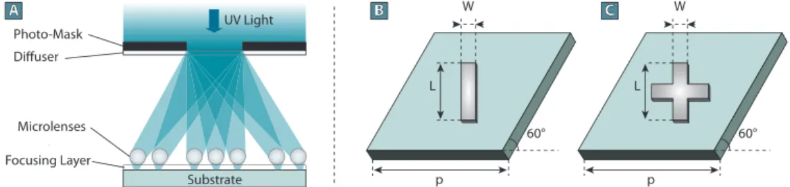
The TEMPL fabrication method (see Fig. 1) takes advantage of an array of microspheres behaving as an array of microlenses, and for which every sphere projects the image of a macroscopic photomask onto a substrate, thus allowing to perform projection lithography with reduction factors of the order of 10 000 × [24]. We have shown that it is possible to pattern those microspheres in any desirable pattern, and thus to fabricate a non-periodic array of microstructures which distribution is set by the distribution of the microspheres, and which local structures are a replica of the structure of the photomask. Our objective, for this paper, is to illustrate the concept of positional gradients and how it allows to design interesting optical materials, but keeping in mind the constraints of the TEMPL fabrication technique, to ensure that the device we propose could be fabricated without much effort. The constraints are essentially two-fold: i) the resolution of the microstructures is limited to that of TEMPL which is of the order of 400 nm, and ii) the distance between identical neighboring structures is limited by the assembly of the microlens array, and the lower limit is therefore that of a close-packed array of microspheres, i.e. with reticular distances equal to the nominal diameter of the microspheres used for TEMPL (in our previous work that is d ~5 µm).
Based on our observation that the arrangement of the microstructures had a strong influence on their resonant frequencies, we simulated periodic hexagonal tilings of microresonators (see Fig. 1) as a proxy for the local behavior of the non-periodic arrays, and studied the variation of their optical spectra as a function of the pitch of the lattice. All of the simulations were performed with CST Microwave Studio, using the frequency-domain solver.
p 60° W L p 60° W L BB A UV Light C Substrate Focusing Layer Microlenses Photo-Mask Diffuser
Fig. 1. Schematic representation of the TEMPL fabrication method (A) and unit cell representations of the simulated periodic materials consisting of silver bars (B) and crossbars (C) on a CaF2 substrate.
In order to have metasurfaces with sharp resonances – which in turn translates in sharp phase signals – we designed resonators made of silver, since the damping coefficient of silver is smaller than that of gold [1]. To ensure a good overall transmittance of the device in the infrared, we used CaF2 as the carrier dielectric substrate. The silver material was simulated
with a Drude model using literature parameters [25] with ωp = 2175 THz and a damping
frequency of ωT = 4.35 THz. To ensure that the designs could potentially be fabricated, we
limited our study to extremely simple local resonant structures (bars and crosses) and adjusted their dimensions to those of the biggest samples fabricated in our previous paper. In particular, we chose to design 50 nm thick dipole antennas of length L = 3500 nm and a width
w = 900 nm. Crossbar structures were obtained as the union of two of those bars at an angle
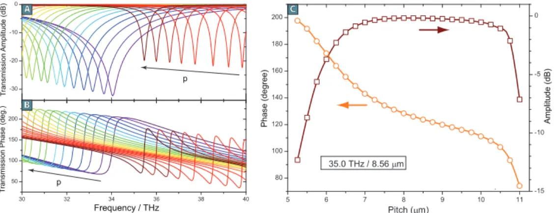
of 90° (see Fig. 1). The resulting spectra are shown in Figs. 2(a) and 2(b), and one can see that in the spectral region we studied, there are two resonant frequencies that were both red-shifted as we increased the pitch of the lattice from 5.25 μm to 11 μm (pitches adapted to the dimensions of the microspheres we used in our experimental study, which had a nominal diameter of 5 μm). Similarly to what is observed in the design of Memarzadeh et al. [16], the interplay between the phase-changes due to the two resonant frequencies, in the spectral region laying in between them, yielded a gradual change of phase delay while maintaining a reasonably high transmission amplitude. The variation of the resulting transmitted phase and amplitude is shown in Fig. 2(c), and with an attenuation range of 0 to −5 dB, one can get a continuous modulation of the phase delay over a range of c.a. 100 degrees. We note however that formally speaking, metasurfaces imply sub-wavelength spacing of the functional units and the device we propose here include, for the most spaced-out features, distances of the order of lambda. Frequency / THz T ransmission Amplitude (dB) Amplitude (dB) T
ransmission Phase (deg.)
Phase (degree) p p A B C
Fig. 2. Transmission (A) and phase (B) spectra for hexagonal arrays of silver microbars on CaF2 presenting two resonant frequencies that are both red shifted as the pitch varies between 5.25 µm and 11 μm in 0.25 µm increments and (C) phase and amplitude modulation at 35 THz – i.e. between the two resonant frequencies – as a function of the pitch of the arrays.
The phase modulation achieved with such a design is far from being spectacular (for general applicability one would want a full 2π phase space) which limits its applicability to small (a few mm2) devices with rather long (a few cm) focal lengths, according to Eq. (1):
2 2 2 2 2 ( , )x y π f x y π ϕ λ λ + = − (1)
where φ is the transmitted phase, λ is the operating wavelength, and x and y are the Cartesian coordinates in the plane of the lens, with respect to its center. For a 2 × 2 mm2 flat
lens with an operating frequency of 35 THz, Eq. (1) can be satisfied in all points of the device, provided that the focal length f is at least 10 cm. The limitations in achievable phase changes arise mostly from the π phase space obtained for a single resonant mode and the damping of the oscillators. We therefore believe that it is possible that using sharp fano-type resonances or stacking multiple thin-layer devices could increase the available phase space to achieve better designs.
For a hexagonal tiling of microbars, the transmitted phase changes monotonously with the lattice spacing (see Fig. 3) and it is therefore possible to design a gradient metasurface in which the phase gradient required for the design of a lens – according to Eq. (1) – can be obtained by mapping a gradient of lattice spacing in order to satisfy Eq. (1) in every point of the array. An illustration of such a device is given in Fig. 3. Locally, in any point of the metasurface, the symmetry is pseudo-hexagonal, but the pitch of that hexagonal tiling is
modulated continuously in a radial fashion from the center of the device. This design should yield polarization-dependent flat lenses as evidenced by the variation of the simulated transmission spectra as a function of the angle between the incident polarization and the main direction of the dipolar microbars (see Fig. 4(a)).
5.5 11
p (
μm)
Fig. 3. Hypothetical flat lens consisting of a gradient metasurface with local hexagonal symmetry but with a radial pitch modulation.
Nevertheless, it can easily be adapted to a polarization-independent device by patterning cross structures instead of bars. As expected, due to the symmetry of the resonant micropattern, the optical behavior is then independent of the incident polarization (see Fig. 4(b)). The resonant frequencies of the crossbar design are slightly blue-shifted with respect to those of the initial bar design (when conserving the overall dimensions), and one can therefore expect that with such a design, it would be necessary to use a different spatial array of micro-structures to have a device obeying Eq. (1).
Frequency / THz Frequency / THz T ransmission Amplitude (dB) T
ransmission Phase (degree)
A B P = 6500 P = 11000 P = 6500 P = 11000 Amplitude / dB Frequency / THz Phase / degree Pitch / µm D C
Fig. 4. Variations in transmission amplitude for the two resonant modes as a function of incident polarization for bar-shaped (A) and crossbar-shaped (B) micro-resonators for an incident polarization angle varying between 0 and 60° in 10° increments, with respect the longitudinal direction. The inserts correspond to the electric field intensity distribution for the two modes involved. (C-D) Comparison of the optical signature of hexagonal arrays of 3.5 µm bar-shaped microstructures and 4.0 µm cross-shaped microstructures (C) and the transmitted phase vs. pitch curves for such arrays (D).
Besides, it would probably perform at a different frequency than the initial device. Nevertheless, one of the main advantages of template-encoded microlens lithography is precisely its ability to produce meta-surfaces with varying local designs in a fast, iterative manner, and one could easily proceed to optimizing the behavior of the system by performing small adjustment to the geometry of the photomasks. Since those masks have millimeter-scale dimensions, they can be produced and adjusted in a matter of minutes. We show that by adjusting slightly the length of the crossbars (from 3.5 µm to 4.0 µm) the resonant frequencies of the crossbar design can be adjusted to match better with those of the bar design and in particular, the resulting phase vs. pitch curves can be made to match with minor deviations (see Fig. 4(c) and 4(d)).
Those two devices can therefore be fabricated with the same non-periodic array of micro-lenses (using different photomasks) to yield similar light-focusing abilities. The design we present here only yields moderate phase changes, and therefore is limited to flat lenses with relatively long focal distances, but it presents a series of advantages over those consisting in a change of the local micro-patterns. For example, the modulation of the phase response of the array of microstructures is a continuous function of the pitch of the array (see Fig. 2(c)), and therefore allows a semi-continuous spatial control of the phase, by interpolation of the pitch-dependent phase and amplitude curves. Also, those designs could be fabricated using the TEMPL lithography method, which was specifically designed to allow for fast prototyping of non-periodic meta-surfaces. This ensures the feasibility of fabricating functional designs based on positional gradients, and of fast iteration and optimization between them by using the same microlens arrays with a simple change of macroscopic photomask.
3. Summary
Altogether, we demonstrate here an original concept for the fabrication of IR optical devices by designing non-periodic positional gradients that, we hope, will allow us to develop original experimental devices in the near future. While some of structures we present here may fall short of the formal definition of metasurfaces, we believe that further development based on this concept could identify designs evidencing similar behavior at shorter lateral spacing. The overall idea is that the phase response of flat optical devices based on metasurfaces could be controlled by patterning a non-periodic distribution of identical resonant microstructures instead of using the conventional method that consists in engineering a phase profile by patterning regular arrays of different local microstructures. We chose to illustrate it with designs for IR metalenses that are either polarization dependent or independent, but it is a more general concept that could in principle be used for general wave-front engineering [13, 17].
Funding
Marie Curie IOF FP7 (SAM-TunEGaIn PIOF-GA-2012-28412); French National Research Agency (ANR) Investment for the Future Programme IdEx Bordeaux (ANR-10-IDEX-03-02).
Acknowledgments
We warmly thank Dr. Alex Nemiroski and Dr. Mahiar M. Hamedi, as well as Prof. Luca del Negro for useful discussions around microlens lithography and non-periodic optics.