Fabrication and characterization of MEMS
alkali vapor cells used in chip-scale atomic
clocks and other atomic devices
Thèse présentée à la Faculté de Sciences de l’Université de Neuchâtel pour
l’obtention du grade de Docteur ès Sciences par :
Sylvain Karlen
Acceptée sur proposition du jury :
Prof. Gaetano Mileti, Université de Neuchâtel, Directeur de thèse
Prof. Nico de Rooij, EPFL, Neuchâtel, Rapporteur
Dr. John Kitching, NIST, Boulder, Colorado (USA), Rapporteur
Dr. Steve Lecomte, CSEM SA, Neuchâtel, Rapporteur
Dr. Pierre Waller, ESTEC, Noordwijk (NL), Rapporteur
Dr. Christoph Affolderbach, Université de Neuchâtel
Dr. Jacques Haesler, CSEM SA, Neuchâtel
Imprimatur pour thèse de doctorat www.unine.ch/sciences Faculté des Sciences
Secrétariat-décanat de Faculté Rue Emile-Argand 11 2000 Neuchâtel – Suisse Tél : + 41 (0)32 718 21 00 E-mail : secretariat.sciences@unine.ch
IMPRIMATUR POUR THESE DE DOCTORAT
La Faculté des sciences de l'Université de Neuchâtel
autorise l'impression de la présente thèse soutenue par
Monsieur Sylvain KARLEN
Titre:
“ Fabrication and characterization of MEMS
alkali vapor cells used in chip-scale atomic
clocks and other atomic devices
”
sur le rapport des membres du jury composé comme suit:
• Prof. Gaetano Mileti, directeur de thèse, Université de Neuchâtel, Suisse
• Prof. Nico de Rooij, EPFL, Neuchâtel, Suisse
• Dr John Kitching, NIST, Boulder, Colorado, United States
• Dr Steve Lecomte, CSEM, Neuchâtel, Suisse
• Dr Pierre Waller, ESA-ESTEC, Noordwijk, Netherlands
• Dr Christoph Affolderbach, Université de Neuchâtel, Suisse
• Dr Jacques Haesler, CSEM, Neuchâtel, Suisse
Abstract
Atomic clocks are timekeeping devices that can achieve extreme performance in terms of stability and accuracy. Behind this name, hides a variety of different systems which size and complexity can be considerably different depending on their applications. The primary frequency standards used for the realization of the second and the clocks mounted on the Galileo satellite positioning system are two well-known examples.
In recent years, considerable efforts lead to miniaturization and reduction of the power consump-tion of such systems, giving rise to the first chip-scale atomic clocks (CSACs). The performance of these devices is potentially superior to high-performance quartz of comparable size. Their manufac-turing is made possible by the use of micro-technology-specific manufacmanufac-turing processes techniques and the use of a purely optical interrogation scheme called coherent population trapping (CPT). At the heart of a CPT clock is the micro-fabricated (MEMS) cell. It consists of a sealed cavity having an optical access and containing an alkali metal vapor as well as a buffer gas. It should however be noted that the use of such MEMS cells is not limited to CSACs but can be extended to other atomic sensors such as atomic gyroscopes and atomic magnetometers.
The present thesis deals with two main subjects of study concerning micro-manufactured atomic cells. First, various aspects related to cells fabrication are reviewed and new micro-fabrication tech-niques are studied. In a second step, the performances of atomic cells manufactured with these techniques are measured for their use in CSACs and atomic gyroscopes.
The first micro-fabrication technology proposed here is the application of copper-copper thermo-compression as an alternative hermetic sealing technology. This method allows to overcome some of the limitation inherent to the established anodic bonding. By limiting the cavity contamination and allowing the bonding of other alternative materials, it potentially allows to lengthen the cell lifetime and improve the long-term clock frequency stability. In particular a preliminary study on the man-ufacturing of the sapphire-sapphire cells is presented and a study of the residual gas contamination inside the cavity is realized.
The second technique of micro-fabrication presented here is the application of an aluminum oxide coating on the inner walls of the cells. This coating allows to reduce the reaction between the alkali metal and the cell walls and to improve their lifetime which is particularly interesting in the case of cells filled by UV-decomposed rubidium azide for which the amount of alkali metal is limited. In this context, a new method for measuring the partial pressure of nitrogen by Raman spectroscopy is presented and compared with a similar measurement carried out by atomic spectroscopy. The results made with this novel technique are used in a lifetime study of cells filled by rubidium azide decomposition and sealed by anodic bonding.
The use of rubidium micro-pills as an alkali metal source is then studied. Cells filled with this method are characterized with respects to their application in CSACs. In particular, a new argon-neon buffer gas mixture developed for this filling method is assessed and the dependence of the atomic frequency to the temperature and its thermal inversion point are studied.
The latest technology studied here is the use of gold micro-disks as preferential nucleation sites for rubidium. By condensing the rubidium out of the laser light-path, these micro-structures prevent the
migration of alkali metal droplets and the induced clock frequency instabilities. Long-term stability studies are therefore presented to highlight this phenomenon and demonstrate the effectiveness of this technology.
Finally, a preliminary characterization of the Xe relaxation time in MEMS cells in presented in view of their use in atomic gyroscopes.
Keywords:
Alkali metal atomic vapor cells, rubidium, microfabrication, atomic clocks, atomic spectroscopy, Raman spectroscopy, image analysis, buffer gas, MEMS, CSAC, atomic gyroscope
Résumé
Les horloges atomiques sont des gardiens de temps pouvant atteindre des performances extrêmes en termes de stabilité et de précision. Sous ce terme, se cache cependant une grande variété de systèmes très différents dont la taille et la complexité peuvent varier considérablement en fonction de leurs applications. On citera par exemple les étalons primaires de fréquence utilisés pour la réalisation de la seconde ou les horloges embarquées dans le système de positionnement par satellite Galileo.
Ces dernières années, des efforts importants de miniaturisation et de réduction de la consommation ont donné naissance aux toutes premières horloges atomiques miniatures dont les performances sont potentiellement supérieures à des quartz de haute performance de taille comparable. La fabrication de telles horloges est rendue possible par l’utilisation de techniques de fabrication spécifiques à la micro-technologie et d’un schéma d’interrogation purement optique appelé piégeage cohérent de population. La partie centrale d’une telle horloge est la cellule micro-fabriquée. Celle-ci consiste en une cavité ayant un accès optique et contenant une vapeur de métal alcalin ainsi qu’un gaz tampon. On notera en outre que leur utilisation n’est pas limitée aux horloges miniatures, mais peut être étendue à d’autres senseurs atomiques tels que les gyroscopes atomiques et les magnétomètres atomiques.
La présente thèse de doctorat s’articule autour de deux principaux sujets d’étude concernant les cellules atomiques fabriquées. Premièrement, différents aspects liés aux techniques de micro-fabrications sont passées en revue et de nouvelles techniques sont étudiées. Dans un second temps, les performances de cellules atomiques fabriquées selon ces techniques sont mesurées afin d’évaluer leur utilisation en micro-horloge ainsi qu’en gyroscope.
La première technologie de micro-fabrication proposée ici est l’application de la thermocompression cuivre-cuivre comme méthode alternative à la soudure anodique pour le scellage hermétique. Cette technique permet de réduire les contaminations internes à la cavité ainsi que d’utiliser des matériaux différents que le silicium et le borosilicate comme constituants de la cellule, allongeant potentiellement leur durée de vie et leur stabilité sur le long-terme. La contamination gazeuse des cellules scellées par thermocompression cuivre-cuivre est en particulier étudiée et une étude préliminaire sur la fabrication de cellules saphir-saphir est présentée.
La deuxième technique de micro-fabrication étudiée est l’application d’un revêtement d’oxyde d’aluminium sur les parois intérieures des cellules. Celle-ci permet de réduire la réaction entre le métal alcalin et les parois des cellules et/ou d’agir comme barrière étanche entre la cavité et le verre et l’extérieur et ainsi d’améliorer leur durée de vie. Cette technologie est en particulier utilisée dans le cas de cellules remplies par décomposition d’azoture de rubidium pour lesquelles la quantité de métal alcalin est limitée. Dans ce cadre, une nouvelle méthode de mesure de la pression partielle d’azote par spectroscopie Raman est présentée et comparée à une mesure similaire réalisée par spectroscopie atomique. Ces résultats sont utilisés dans le cadre d’une étude de durée de vie de cellules remplies par cette méthode et scellées par soudure anodique.
L’utilisation de micropilules rubidium comme source de métal alcalin est ensuite étudiée. Des cellules de ce type sont caractérisées selon plusieurs aspects. En particulier un nouveau mélange de gaz tampon argon-néon développé pour cette méthode de remplissage est examinée et la dépendance de la fréquence atomique à la température et le "point d’inversion" thermique sont étudiés.
La dernière technologie décrite est l’utilisation de micro-disques en or comme point de nucléation du rubidium. En condensant le rubidium hors du chemin optique du laser, ceux-ci permettent d’éviter la migration de gouttelettes de métal alcalin et les instabilités de fréquence d’horloges induites. Des études de stabilité long-terme sont présentées pour mettre en évidence phénomène et prouver l’efficacité de cette technologie.
Finalement, une étude préliminaire sur le temps de relaxation du xénon dans des cellules micro-fabriquées est présentée en vue de leur utilisation dans des gyroscopes atomiques.
Mots clés :
Cellules atomiques à vapeur de métal alcalin, rubidium, micro-fabrication, horloges atomiques, piégeage cohérent de population, spectroscopie atomique, spectroscopie Raman, analyse d’image, gaz tampon, gyroscopes atomiques
Acknowledgement
I would like to thank all the people who have helped, guided, advised or supported me, directly or indirectly, during the realization and the writing of this thesis:
• First and foremost, I would like to express my sincere gratitude to Dr. Jacques Haesler and Dr. Steve Lecomte, my supervisors at CSEM where I performed most of my research. Their availability, enthusiasm and expertise helped me in all the time of research and writing of this thesis. I could not have imagined having better advisors and mentors for my PhD study. • My sincere thanks goes to my thesis director and supervisor at the University of Neuchâtel,
Prof. Gaetano Mileti, for the continuous support of my study and related research, for his advices and great knowledge. His guidance greatly helped me in the structuring of my research and writing of this thesis.
• Besides my supervisors, I would like to thank the rest of my thesis experts committee: Prof. N. de Rooij, Dr. John Kitching, Dr. Pierre Waller and Dr. Christoph Affolderbach , for their insightful comments and encouragement, but also for the questions which encouraged me to widen my research from various perspectives.
• A very special thank goes to my colleagues from the Time and Frequency sector at CSEM and in particular Dr. Laurent Balet, Dr. Gilles Buchs, Dr Dmitri Boiko and Dr. Stefan Kunderman whose availability, kindness and motivation helped me with the technical aspects of my thesis and more generally all my colleagues from the Systems division at CSEM.
• I would also like to show my gratitude to Dr. Thomas Overstolz and Dr. Jean Gobet who supervised and guided me through all the technical aspects of MEMS fabrication and charac-terization. Their huge expertise in the domain allowed to orient my research in a much faster path toward its goal. The results presented here could not have been obtained without their help.
• A special thank also goes to the technical staff of the clean room and to my other colleagues of the Micro & Nano Systems division at CSEM in particular Giovanni Bergonzi but also Mehretab Amine, Florence Rigoletti, Sylviane Pochon, Pierre-André Clerc, Stéphane Ischer, Angélique Bionaz, Dr. Mohammad Mehdi Dadras, Silvia Biselli and Dr. Kaushik Vaideeswaran. Their knowledge and availability was an invaluable help.
• During my stay at ESTEC, I had the chance to collaborate with the time and frequency best-in-class people in the space domain. Thereby, I would like to thank Dr. Pierre Waller and Marco Belloni but also Dr. Piero Angeletti and the other members of the RF Equipment & Technology Section at ESA ESTEC for their warm welcome and the vast experience they shared with me during the three months I spent with them.
• During my PhD study, I also had the chance to collaborate directly with the members of the Time and Frequency Laboratory at the Universtiy of Neuchâtel and to use their research facilities. Thereby, I would like to thank Dr. Matthieu Pellaton, Dr. Renaud Matthey, Dr. Stéphane Schilt, Mohammadreza Gharavipour and William Moreno for the experience they shared with me and for the fruitful discussion we had.
• Last but not least, I want to thank my family and my friends (some are also colleagues) for their support, love and affection through the years spent on my PhD study but also before and after that.
Sylvain Karlen
This work could not be realized without the financial support of CSEM internal funding, financed by the canton of Neuchâtel and the Swiss confederation and of the European Space Agency (ESA) under the Networking/Partnering Initiative (NPI), ESA Contract No. 4000112650/14/NL/GLC.
Contents
Imprimatur i Abstract iii Résumé v Acknowledgement vii Table of contents ixList of figures xiii
List of tables xvii
Author’s contribution xix
Abbreviations xxi
1 Introduction 1
1.1 Scope and objective . . . 1
1.2 Basic operating principle of an atomic clock . . . 3
1.3 Chip-scale atomic clock and MEMS atomic vapor cells: State of the art . . . 4
1.3.1 Early development . . . 4
1.3.2 Internal alkali dispenser . . . 5
1.3.3 Low-temperature bonding for cells with anti-relaxation coating . . . 6
1.3.4 Functionalized cells . . . 6
1.3.5 Long light-path microfabricated cells . . . 6
1.3.6 Atomic vapor cells for magnetometers . . . 6
1.3.7 Other related publications . . . 7
1.4 Summary . . . 7
2 Physics of Rb atomic vapor cells 9 2.1 Coherent Population Trapping: Description of the phenomenon . . . 9
2.2 Structure of the Rb atom . . . 10
2.2.1 Fine structure . . . 11
2.2.2 Hyperfine structure . . . 12
2.2.3 Zeeman splitting . . . 12
2.3 Optical absorption of rubidium . . . 14
2.3.1 Relative transition strength . . . 14
2.3.3 Absolute absorption . . . 16
2.4 Spectroscopy of the CPT resonance . . . 17
2.4.1 CPT amplitude and linewidth . . . 17
2.4.2 Ground state relaxation in Rb cells . . . 18
2.5 Atomic clock frequency stability . . . 19
2.5.1 Allan deviation . . . 19
2.5.2 Short term frequency stability . . . 19
2.5.3 Frequency shift and long-term stability . . . 20
2.5.4 Influence of the physical parameters on the short term stability . . . 23
2.6 Requirements for rubidium cells for chip scale atomic clock . . . 24
2.6.1 Overall clock requirements . . . 24
2.6.2 Critical review of the requirements . . . 26
2.7 Nuclear magnetic resonance in alkali vapor cells . . . 29
2.7.1 Nuclear magnetic gyroscopes: general principle . . . 29
2.7.2 Spin-exchange optical pumping . . . 30
2.7.3 The alkali metal used as magnetometer . . . 31
2.7.4 Detection of the Xe relaxation . . . 32
2.8 Conclusion . . . 33
3 Microfabrication of atomic vapor cells 35 3.1 Review of fabrication techniques and materials . . . 35
3.1.1 Materials . . . 35
3.1.2 Bonding technology . . . 39
3.1.3 Dispensing technique . . . 44
3.1.4 Getters and anti-diffusion surface coating . . . 48
3.2 Cu-Cu thermocompression bonded cells . . . 49
3.2.1 Substrate structuration . . . 50
3.2.2 Copper metalization . . . 50
3.2.3 Thermocompression bonding . . . 51
3.2.4 Optimization of the bonding process . . . 52
3.2.5 Sapphire cells . . . 55
3.2.6 Complete cell realization . . . 57
3.3 Alkali dispensing . . . 61
3.3.1 Alkali azide decomposition . . . 61
3.3.2 Dispensing micro-pill . . . 61
3.4 Anti-diffusion surface coating . . . 63
3.5 Gold micro-discs . . . 63
3.5.1 Working principle . . . 63
3.5.2 Gold surface structuration . . . 64
3.5.3 Cell fabrication . . . 65
3.5.4 Microscope imaging . . . 65
3.6 Conclusion . . . 67
4 Spectroscopic characterization of MEMS atomic vapor cells 69 4.1 CPT hyperfine frequency spectroscopy . . . 69
4.1.1 Setup description . . . 69
4.1.2 Determination of cell intrinsic frequency . . . 71
4.1.3 Temperature dependence of Ar - Ne cells frequency . . . 73
4.1.4 Contrast and FWHM of Ar - Ne cells . . . 75
Contents
4.1.6 Pressure determination for Ar - N2 cells . . . 77
4.1.7 Contrast and FWHM of Ar - N2cells with isotopically selected87Rb . . . 78
4.2 Nitrogen partial pressure determination by Raman spectroscopy . . . 79
4.2.1 Description of measurement . . . 79
4.2.2 Comparison of results . . . 81
4.3 Vacuum level assessment by Doppler-free absorption spectroscopy . . . 82
4.3.1 Setup description . . . 82
4.3.2 Cu-Cu thermocompression bonding cells . . . 83
4.4 Preliminary measurement of Xe relaxation . . . 85
4.5 Conclusion . . . 87
5 Analysis of RbN3-filled MEMS cells lifetime 89 5.1 Alkali consumption model . . . 89
5.2 Measurement of metallic rubidium amount . . . 90
5.3 Calibration of droplets volume and measurement of the initial consumption . . . 91
5.4 Cell lifetime estimation . . . 92
5.5 Conclusion . . . 93
6 Clock measurement of long-term stability 95 6.1 Clock setup . . . 95
6.1.1 Description of the setup . . . 95
6.1.2 Laser head characterization . . . 97
6.2 Long term measurement on cells with and without gold micro-discs . . . 105
6.2.1 Evidence of instabilities due to Rb droplets migration . . . 105
6.2.2 Comparison between measurement with and without gold micro-discs . . . 109
6.3 Conclusion . . . 112 7 Conclusion 113 7.1 Major results . . . 113 7.2 Future outlook . . . 114 Bibliography 129 Curriculum vitae 131
List of Figures
1.1 Basic operating principle of a passive atomic clock . . . 3 1.2 Coherent population trapping and double resonance interrogation scheme . . . 3 2.1 Three level system considered for the explanation of the coherent population trapping
phenomena . . . 9 2.2 Gross, fine and hyperfine structure of Rb D lines in absence of external magnetic field 14 2.3 Noise sources affecting the short term frequency stability in function of the optical
intensity . . . 21 2.4 Ground population relaxation rate in function of the buffer gas pressure . . . 24 2.5 Barometric relative frequency shift coefficient in a cylindrical cell for Pyrex and sapphire 28 2.6 Full clock frequency stability requirements: ESA requirements and extrapolation on
full time range based on the most stringent requirements . . . 29 2.7 Polarization of idealized Rb vapor by D1 optical pumping withσ+light . . . 30 2.8 Alkali metal dipole ensemble in three cases depending on the magnetic field . . . 32 2.9 Oscillation of the alkali metal magnetic moment in zero and low field configurations . 33 3.1 Permeability of quartz and Pyrex®to H
2and He versus wall temperature . . . 37
3.2 3D model of a two Cu-Cu thermocompression cell filled with a Rb dispensing micro-pill 49 3.3 Thermocompression cell layers design: cavity, cavity and channels DRIE, TTV release
and Cu structuration . . . 50 3.4 Cr Cu etch test: Cu layer nearly fully under-etched at the time Cr etching is completed 51 3.5 Simplified thermocompression bonding test process . . . 52 3.6 Example of a bonding sample of run 2 after the pull test: The Cu layer did not adhere
to the glass substrate . . . 53 3.7 SEM analysis of a test wafer with Cr adhesion layer after bonding tentative at 400°C . 55 3.8 SEM cross-section measurement made on a sample bonded at 400°C . . . 56 3.9 Bonding test of silicon on sapphire: silicon substrate broken due to the too high CTE
difference . . . 56 3.10 Through-hole cavities and 100µm deep, 100µm wide micro-channels machined in a
500 µm thick sapphire wafer . . . 57 3.11 Full microfabrication process of the Cu-Cu thermocompression cells . . . 59 3.12 Monitoring of the bonding parameters during the second bonding step of a Cu-Cu
thermocompression wafer . . . 60 3.13 Picture of the first realization of a Cu-Cu thermocompression atomic vapor cell: cell
after dicing and wafer-level view . . . 60 3.14 Schematic view of the micro-pill activation setup . . . 62 3.15 Example of a cell with excess Rb due to a too high laser intensity and too long
activation time . . . 62 3.16 Au-Rb phase diagram - Copyright ©1986, American Society for Metals. Reprint by
3.17 Anodic bonded cell with Au micro-discs layers design: cavity, cavity and channels
DRIE, Au structuration . . . 64
3.18 Microfabricated cell with Au microdiscs . . . 65
3.19 Microfabrication process of the anodically bonded cells with Au discs tested in the frame of the present work . . . 66
3.20 Measurement cavity of a MEMS cell with Au micro-discs: cavity right after activation, same cavity after heating of the cell on a hot plate during 4 hour, same cavity after a thermal treatment of 1h at 180°C. . . 67
4.1 Buffer gas pressure measurement setup used for the hyperfine shift measurement technique . . . 70
4.2 Zeeman spectrum measured on a (natural) RbN3filled Ar-N2 MEMS cell . . . 71
4.3 CPT signal measured on an anodic bonding, natural Rb, dispensing micro-pill, Ar-Ne MEMS cell . . . 72
4.4 0-light shift extrapolation of CPT clock frequency shift for a natural Rb, dispensing micro-pill, Ar-Ne MEMS cell . . . 73
4.5 Temperature dependence of the buffer gas frequency shift for run 1 . . . 74
4.6 Temperature dependence of the buffer gas frequency shift for run 2 . . . 74
4.7 CPT spectroscopic parameters for a cell filled with 150 mbar Ar-Ne buffer gas (run 1), measured on the85Rb isotope of natural Rb . . . 75
4.8 CPT spectroscoic parameters for a cell filled with 100 mbar Ar-Ne buffer gas (run 2), measured on the85Rb isotope of natural Rb . . . 76
4.9 CPT signal measured on a Cu-Cu thermocompression bonding, natural Rb, dispensing micro-pill, Ar-Ne MEMS cell . . . 77
4.10 Fitting of the Ar - N2buffer gas shift example on a natural RbN3 filled MEMS cell . . 77
4.11 CPT spectroscopic parameters for a87Rb cell filled with Ar-N 2buffer gas . . . 78
4.12 Scheme of the Raman spectroscopy experiment - Copyright © 2017 SAGE Publication. Reprint by permission of SAGE Publication. . . 79
4.13 Example of Voigt profile used to fit the Raman Q branch of N2- Experimental data: courtesy of Jean Gobet, CSEM . . . 80
4.14 Experimental µ-Raman spectra used for N2 pressure measurement: Calibration in atmosphere, calibration in Ar and measurement inside a sealed MEMS cell cavity -Experimental data: courtesy of Jean Gobet, CSEM . . . 81
4.15 Comparison between the N2 partial pressure determined by Raman spectroscopy and the N2 partial pressure determined by CPT spectroscopy and Tukey mean-difference plot - Raman experimental data: courtesy of Jean Gobet, CSEM . . . 82
4.16 Doppler-free absorption spectroscopic setup . . . 83
4.17 Doppler-free absorption spectrum example: data, fit and full spectrum . . . 84
4.18 0-light extrapolation of the selected Doppler-free fitted linewidth . . . 84
4.19 Picture of the Xe spin relaxation time measurement setup . . . 85
4.20 Schematic of the Xe spin relaxation time measurement . . . 86
4.21 Xe NMR signal measured in a MEMS cell and FFT of the signal . . . 86
5.1 Example of the evolution of the amount of rubidium for two cells with and without Al2O3coating . . . 90
5.2 Image recognition of Rb droplets size in MEMS atomic vapor cell: microscope image of a cell and extraction of drop radius by image recognition software - Microscope image: courtesy of Jean Gobet, CSEM - Copyright © 2017 Optical Society of America. Reprint by permission of Optical Society of America. . . 91
5.3 Example of the droplets evolution over time for a cell- Microscope image: courtesy of Jean Gobet, CSEM - Copyright © 2017 Optical Society of America. Reprint by permission of Optical Society of America. . . 91
List of Figures
5.4 Spherical cap model used for Rb drop volume estimation . . . 91
5.5 Estimation of Rb initial consumption: The contact angleθ is adapted such that the slope is 1 for the non-0 values of the measured Rb quantity . . . 92
5.6 Estimation of the activation energy by fitting of the rubidium consumption rates of cells at different temperatures . . . 93
6.1 Schematic view of the long-term measurement setup: laser power and frequency servo loops and parameters monitoring . . . 96
6.2 Schematic view of the physical implementation of the long-term measurement setup . 96 6.3 Fabry-Pérot and Optical spectrum analyzer setup . . . 97
6.4 Laser temperature necessary to reach the 87Rb D1 line as a function of the laser injection current for the long-term setup laser . . . 98
6.5 Laser spectrum and SMSR definition . . . 98
6.6 SMSR dependency to the laser injection current for the long-term setup laser . . . 99
6.7 Laser linewidth measurement: data from the Fabry-Pérot interferometer and Lorentzian fit. . . 100
6.8 Laser beam profiles at cell position for the long-term setup laser . . . 100
6.9 Laser power dependance to the injection current for the long-term setup laser . . . 101
6.10 Laser power dependance to the temperature for the long-term setup laser . . . 101
6.11 Laser wavelength dependance to the injection current for the long-term setup laser . . 102
6.12 Laser wavelength dependance to the temperature for the long-term setup laser . . . . 103
6.13 Dependance of the Laser sidebands intensity to the injected RF power for the long-term setup laser . . . 103
6.14 Dependance of the Laser sidebands intensity to the injection current for the long-term setup laser . . . 104
6.15 Dependance of the Laser sidebands intensity to the temperature for the long-term setup laser . . . 105
6.16 Comparison between the output power and the relative clock frequency for the MEMS cell without Au micro-disc . . . 107
6.17 Allan Variance measured for the MEMS cell without Au micro-disc and calculated influence of the different experimental parameters . . . 108
6.18 Allan Variance measured for the MEMS cell with Au micro-discs and calculated influ-ence of the different experimental parameters . . . 110
6.19 Comparison between two clocks realized with cells containing or not gold micro-discs . 111 6.20 Comparison between the two clock frequency along the long-term measurement . . . . 112
List of Tables
1.1 Summary of the different types of MEMS atomic vapor cells characterized in the frame of the present work . . . 2 1.2 Comparison of the long-term frequency stability achieved by the different research
groups in the world . . . 8 2.1 Relative abundance and first and second order Zeeman shifts for85Rb and87Rb . . . . 14
2.2 Strength factor for the transitions for the87RbD1 line -C2
F . . . 15
2.3 Optical broadening coefficients of typical gases for the D1 and D2 lines of Rb . . . 16 2.4 Buffer gas collision cross section for Rb for population relaxation . . . 18 2.5 Rubidium diffusion constant in different buffer gases at T0=100°C and P0=760 torr . 18
2.6 Collisional shift coefficients for87Rb atT0= 333K . . . 22
2.7 Full clock specification target . . . 25 2.8 Gyromagnetic ratio for Rb and Xe most common isotopes . . . 30 3.1 Summary of the different Rb-metal systems for the most common solder metals . . . . 38 3.2 Comparison of the most common glass-silicon bonding technology . . . 39 3.3 Summary of the different chemical reactions used for the production of alkali metals . 45 3.4 Bonding test runs and pull test results . . . 54 3.5 Dependency of the buffer gas frequency shift to temperature for Rb at 95°C . . . 62 6.1 Clock frequency dependance to parameters for a MEMS atomic vapor cells filled with
87RbN
3and sealed by anodic bonding . . . 106
6.2 Clock frequency dependance to parameters for a MEMS atomic vapor cells with Au micro-discs filled with natural Rb dispensing micro-pill and sealed by anodic bonding . 109
Author’s contribution
Articles in peer-reviewed journals
[1] S. Karlen, J. Gobet, T. Overstolz, J. Haesler, and S. Lecomte. Lifetime assessment of RbN3-filled
MEMS atomic vapor cells with Al2O3 coating. Optics express, 25(3):2187–2194, 2017.
[2] S. Karlen, J. Gobet, T. Overstolz, J. Haesler, and S. Lecomte. Quantitative micro-Raman spec-troscopy for partial pressure measurement in small volumes. Applied Specspec-troscopy, 71(12):2707– 2713, 2017.
International conferences with proceedings
[1] S. Karlen, J. Gobet, T. Overstolz, and J. Haesler. Non-destructive MEMS atomic vapor cells characterization by Raman spectroscopy and image analysis. In 29th European Frequency and
Time Forum (EFTF), York, United Kingdom, 2016. IEEE.
[2] S. Karlen, J. Haesler, T. Overstolz, G. Bergonzi, and S. Lecomte. Cu-Cu thermocompression bonding as an innovative sealing method for MEMS atomic vapor cells. In ESA Workshop on
Microwave Technology and Techniques (MTT), Noordwijk, The Netherlands, 2017.
[3] S. Karlen, G. Buchs, T. Overstolz, N. Torcheboeuf, E. Onillon, J. Haesler, and D. Boiko. MEMS atomic vapor cells for gyroscope applications. In International Frequency Control Symposium
(IFCS), Joint with the 31st European Frequency and Time Forum (EFTF), pages 315–316,
Be-sançon, France, 2017.
[4] S. Karlen, J. Haesler, T. Overstolz, G. Bergonzi, and S. Lecomte. MEMS atomic vapor cells sealed by Cu-Cu thermocompression bonding. In International Frequency Control Symposium (IFCS),
Joint with the 31st European Frequency and Time Forum (EFTF), pages 625–627, Besançon,
France, 2017.
[5] J. Haesler, K. Kautio, L. Balet, S. Karlen, T. Overstolz, and B. Gallinet. Ceramic based flat form factor miniature atomic clock physics package ( C-MAC ). In ESA Workshop on Microwave
Technology and Techniques (MTT), Noordwijk, The Netherlands, 2017.
[6] J. Haesler, K. Kautio, L. Balet, S. Karlen, T. Overstolz, and B. Gallinet. Ceramic based flat form factor miniature atomic clock physics package ( C-MAC ). In International Frequency Control
Symposium (IFCS), Joint with the 31st European Frequency and Time Forum (EFTF), pages
55–56, Besançon, France, 2017.
[7] G. Buchs, S. Karlen, T. Overstolz, N. Torcheboeuf, E. Onillon, J. Haesler, and D. Boiko. Nuclear spin decoherence time in MEMS atomic vapor cells for applications in quantum technologies. In
[8] J. Haesler, L. Balet, S. Karlen, T. Overstolz, B. Gallinet, S. Lecomte, F. Droz, K. Kautio, P. Karioja, and M. Lahti. Ceramic based flat form factor miniature atomic clock physics package ( C-MAC ). In 6th International Colloquium on Scientific and Fundamental Aspects of GNSS /
Galileo, Valencia, Spain, 2017.
Articles in preparation
[1] S. Karlen, J. Gobet, F. Droz, T. Overstolz, J. Haesler, and S. Lecomte. Reduction of light-shift induced long-term frequency instabilities in alkali vapor cell clock by Au microdiscs.
[2] S. Karlen, J. Haesler, T. Overstolz, G. Bergonzi, and S. Lecomte. Rubidium MEMS atomic vapor cells sealing by Cu-Cu thermocompression bonding.
Abbreviations
AM Amplitude modulation
BHF Buffered hydrofluoric acid
CAD Computer aided design
C-MAC Ceramic miniature atomic clock
CMOS Complementary metal-oxide-semiconductor
CO Cross-over
CPT Coherent population trapping
CSAC Chip-scale atomic clock
CSEM Centre suisse d’électronique et de microtechnique
CTE Coefficient of thermal expansion
DBR Distributed Bragg reflector
DFB Distributed feedback laser
DC Direct current
DRIE Deep reactive ion etching
ESA European space agency
ESTEC European space research and technology center (ESA)
FFT Fast Fourier transform
FIB Focused ion beam
FM Frequency modulation
FoM Figure of merit
FWHM Full width at half maximum
KOH Potassium hydroxide
LS Light-shift
LTCC Low temperature co-fired ceramic
LTF Laboratoire temps-fréquence (University of Neuchâtel)
MAC Miniature atomic clock
MAC-TFC MEMS atomic clocks for timing, frequency control and communications
MEMS Microelectromechanical system
mTS Miniaturized Timing Source
MVD Molecular vapor deposition®
NEG Non evaporable getters
NMP N-Methyl-2-pyrrolidone
NMR Nuclear magnetic resonance
NMRG Nuclear magnetic resonance gyroscope
NTC Negative temperature coefficient (thermistor)
OCXO Oven-controlled crystal oscillator
PD Photodiode (or photodetector)
PER Polarization extinction ratio
PID Proportional integral derivative (controller)
PP Physics package
RF Radio frequency
RIE Reactive ion etching
RQ Requirement
SEM Scanning electron microscope
SEOP Spin-exchange optical pumping
SMSR Side mode suppression ratio
SOA State-of-the-art
TLP Transient liquid phase
TN Technical note
TTV Total thickness variation
UV Ultra-violet
1
Introduction
1.1 Scope and objective
The present work represents the outcome of the research performed on the subject of MEMS atomic vapor cells for chip-scale atomic clocks and other atomic devices at CSEM SA (Centre Suisse d’Électronique et de Microtechnique), a private, non-profit Swiss research and technology organi-zation. It was realized under the supervision of the University of Neuchâtel between August 2014 and December 2017 under the financing of CSEM internal funding, financed by the canton of Neuchâ-tel and the Swiss confederation and by the European Space Agency (ESA) under the Network-ing/Partnering Initiative (NPI). In the frame of this program, a 3 month internship at ESA ESTEC (European Space Research and Technology Center) in Noordwijk, the Netherlands was performed.
MEMS (microelectromechanical systems) atomic vapor cells consist in sealed cavities having an optical access. They are filled with an alkali metal vapor and possibly with other gases. Cur-rent applications are found in chip-scale atomic clocks (CSACs) [1], atomic magnetometers [2] and atomic gyroscopes [3]. Here, various aspects related to cells fabrication are reviewed and new micro-fabrication techniques are studied. Moreover, the performances of atomic cells manufactured with these techniques are measured for their use in CSACs and atomic gyroscopes. The different types of MEMS cells characterized in the frame of the present work are summarized in Tab. 1.1
In the first chapter of this document, a general overview of the working principle of an atomic clock is given. A particular attention is given to the two main interrogation techniques for atomic vapor cell clocks. The different scientific publications on the subject of microfabricated atomic vapor cells for chip scale atomic clock and other atomic devices are then reviewed. The early developments realized in the USA from 2002 to 2008 with the first anodically bonded atomic vapor cell are described. The focus is then given on one of the main research directions taken in Europe which is the use of internal alkali metal dispenser for the cell filling. The researches undertaken on low-temperature bonding and in particular indium bonding for cells with anti-relaxation coatings is then reviewed. The cell functionalization technique proposed by CSEM is then discussed as well as the research made on long light-path cells. Finally, an overview of the publications that were not treated so-far is realized.
The second chapter of this document presents the theoretical aspects in relation with the MEMS atomic vapor cells for CPT atomic clocks and atomic gyroscopes. A general description of the coherent population trapping (CPT) phenomena is given. The structure of the Rb atom is then presented. Details on the optical absorption of rubidium are then given as well as the different relevant aspects for the spectroscopy of the CPT resonance. The link is made with the atomic clock frequency stability and the influence of the different parameters. Based on the requirements for a full chip-scale atomic clock given by ESA, the requirements for a MEMS atomic vapor cell are extracted. The impact of these requirements on particularly relevant technological aspects are deduced. Finally, the theoretical aspects in relation with nuclear magnetic resonance gyroscopes and in particular the
Bonding
technology Isotope Fillingmethod Buffergas Coating Other Chap.Sec. /
Anodic 87Rb RbN
3 Ar-N2 - - 5.1, 4.1.7
Anodic 87Rb RbN
3 Ar-N2 Al2O3 - 5, 6.2.1
Anodic natural Rb RbN3 Ar-N2 Al2O3 - 4.1.6, 4.2
Anodic natural Rb dispensing
micro-pill Ar-Ne Al2O3 - 4.1.3, 4.1.4
Anodic natural Rb dispensing
micro-pill Ar-Ne Al2O3 Au micro-dics 6.2.2
Cu-Cu
thermo-compression natural Rb dispensingmicro-pill Ar-Ne Al2O3 - 4.1.5
Cu-Cu
thermo-compression natural Rb dispensingmicro-pill - Al2O3 - 4.3
Anodic natural Rb RbN3 N2-Xe Al2O3 4 mm diameter
cavity 4.4
Table 1.1: Summary of the different types of MEMS atomic vapor cells characterized in the frame of the present work. "RbN3" stands for RbN3 UV-decomposition. If not otherwise mentioned, the
measurement cavity is 2 mm diameter. A simple cavity design is used with RbN3UV-decomposition
and a two cavity design is used with dispensing micro-pills.
measurement of xenon nuclear spin decoherence time is reviewed.
The third chapter of this document focuses on the microfabrication of atomic vapor cells. A detailed literature review on microfabrication techniques applied to MEMS atomic vapor cells is given. In particular the materials, bonding technologies, alkali dispensing methods, getters and anti-permeation techniques are review. Based on the conclusion of the requirements and of the literature review, different cells design are proposed and their microfabrication is described. In particular, Cu-Cu thermocompression as sealing method, alkali azide and Rb micro-dispensing pills as filling method, Al2O3 as anti-permeation barrier and CSEM patent pending gold micro-discs as alkali preferential
condensing spots are explored.
The fourth chapter describes the different spectroscopic characterization realized on MEMS atomic vapor cells which fabrication is described in the third chapter. The methods used to char-acterize the gas content of MEMS cells is presented: first CPT hyperfine frequency spectroscopy is used. Ar-Ne cells are measured in order to determine the buffer gas pressure as well as its depen-dance to temperature and to find the thermal inversion point. The CPT contrast and linewidth are moreover measured for different temperature and light intensity and the optimal working conditions are determined for Ar-Ne and Ar-N2cells. A preliminary measurement of a CPT signal in Cu-Cu
ther-mocompression bonding cell is presented as well. Secondly, micro-Raman spectroscopy is presented. This technique is used as a fast technique to measure the N2partial pressure inside Ar-N2RbN3filled
cells. The results are compared with CPT hyperfine frequency spectroscopy results made on same cells. Saturated absorption spectroscopy measurements used to assess the vacuum level in evacuated Cu-Cu thermocompression bonded cells are then presented. Finally, preliminary measurements of Xe nuclear spin decoherence time in cells dedicated to gyroscope application are outlined as well as the setup used for it.
The fifth chapter describes the lifetime estimation made on Al2O3 coated MEMS atomic vapor
cells filled with RbN3UV decomposition and sealed by anodic bonding. The main failure mode being
identified as disappearing of metallic alkali metal inside the cell, first a consumption model used to estimate the evolution of the alkali metal amount inside the cell is presented. The image analysis
1.2. Basic operating principle of an atomic clock method used to measure this amount over time is then presented and a total lifetime is estimated.
The sixth and last chapter describes the long-term frequency stability measurement realized of MEMS atomic vapor cells in clock operation. A first measurement realized on a classical MEMS cell evidences that the main source of long-term instabilities is due to migration of alkali droplets on the cell window. Therefore, a second measurement shows that the Au micro-disc solution proposed in the third chapter allows to circumvent this limitation and enhance the long-term frequency stability of CPT clocks realized with microfabricated atomic vapor cells.
1.2 Basic operating principle of an atomic clock
The basic operating principle of a vapor cell atomic clock is shown on Fig. 1.1. It consists of a local oscillator (quartz) and a group of atoms (Rb or Cs). The output frequency of a quartz is servo controlled and locked to the frequency of an atomic transition between two atomic levels of the atoms. The frequency stability of the atoms is therefore transferred to the quartz giving the atomic clock its excellent frequency stability over time.
~
Local oscillator
Atoms
Output
Figure 1.1: Basic operating principle of a passive atomic clock
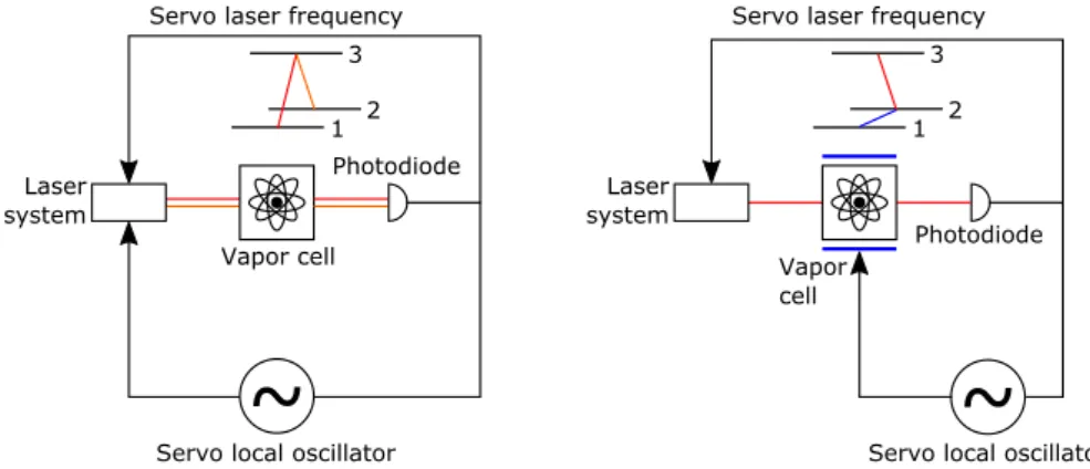
The selected atomic transition is typically the transition between the hyperfine ground-states levels of the atoms. The quartz frequency (in the MHz range) must therefore be converted to the GHz range in order to interrogate the hyperfine frequency of the atoms. Moreover, in cell clocks, a third level is required in order to interrogate the atoms. This third level is typically an excited state of the atom separated from the ground states by an optical transition. Two interrogation schemes are commonly used for interrogation: Double Resonance (DR) or Coherent Population Trapping(CPT).
~
Vapor cell Laser system 1 2 3Servo local oscillator Servo laser frequency
~
Vapor cell Laser system 1 2 3Servo local oscillator Servo laser frequency
Photodiode
Photodiode
Figure 1.2: Coherent Population Trapping interrogation scheme (left) and Double Resonance inter-rogation scheme (right) - The fluorescence can also be detected in the case of CPT.
an optical field (see Fig. 1.2 right). The microwave field, created by multiplication of the quartz frequency, is resonant with the atom hyperfine frequency. The optical field is used to interrogate the absorption between one of the ground states and the excited state and is locked to this transition. Due to absorption, the light field depopulates the observed ground state level which increases the transmission. When the microwave frequency is resonant with the hyperfine frequency, the observed ground state level is repopulated and the transmission decreases. This phenomenon creates an absorption peak on which the quartz frequency can be servo controlled. A detailed description of the phenomena can be found in [4].
In the CPT interrogation scheme, a bichromatic optical field with a frequency difference in the GHz range is applied to the atoms (see Fig. 1.2 - left). The microwave frequency is obtained by the multiplication of the quartz frequency and the generated optical fields are servo controlled to be resonant with the optical transition between the ground states and the excited state. When the frequency detuning between the two components of the bichromatic light field is resonant with the hyperfine frequency, a coherent effect traps the atoms in a so-called dark state. As a consequence, the absorption reduces. As in the DR scheme, the quartz frequency can the be servo controlled to this peak. A detailed description of this effect can be found in Chap. 2.
These two continuous-wave (CW) interrogation techniques imply a high level of coupling between the microwave frequency and the optical field which implies a transfer of laser instabilities to the clock transition. Pulsed schemes were therefore proposed inspired by the Cs beam tube working principle [5]. Pulsed schemes however require a more complex setup with an acousto-optical modulator (AOM) or any other light shutters for the clock operation. They are therefore not excellent candidate for chip-scale atomic clock with a high level of integration and will not be described here.
1.3 Chip-scale atomic clock and MEMS atomic vapor cells:
State of the art
1.3.1 Early development
The early development of a chip-scale atomic clock were realized in 2002 [6]. The requirements for the overall device were a volume of 1 cm3, a short term frequency stability of1·10−11at 1h integration
time and a total power consumption of 30 mW. As the total clock dimensions are relatively small, these requirements are transferred to the atomic cell for which a maximal volume of 5 mm3 is
allowed. Such small cells cannot be realized with the conventional glass blowing technology. The MEMS technology is therefore the best way to produce such small size cells. Anodically bonded cells with a stacking of glass, DRIE etched silicon and glass were then realized. As the filling technique of the cells was still not developed, these cells were linked to an external glass blown tube and filled using cesium with conventional distillation techniques.
The first fully microfabricated atomic vapor cell was realized by NIST in 2004 [7]. As for the first prototypes, the cell was composed of an etched silicon wafer, anodically bonded to two Pyrex wafers. Two etching techniques were compared (DRIE and KOH) as well as two cesium filling techniques: Barium azide decomposition technique (see Sec. 3.1.3.2) and direct dispensing (see Sec. 3.1.3.3). End of 2004, cells of the second type were used to build the first microfabricated atomic clock ever demonstrated [1], and later the same year the first microfabricated magnetometer based on MEMS atomic vapor cells was demonstrated [2].
As the Barium azide decomposition technique showed some long term stability issues, in 2005 a new filling technique was tested by NIST with rubidium which basically moved the barium azide decomposition to the outside of the cell [8]. This improved the cell purity and therefore its long term performances. A relative drift value of 5 · 10−11/day could then be reached. In 2007 finally, a new
1.3. Chip-scale atomic clock and MEMS atomic vapor cells: State of the art 3.1.3.2).
On a commercial point of view, the SA.45s CSAC was released in 2011 by the commercial company Symmetricom1with a total volume of 16 cm3, a full clock short term frequency stability of 2.5 · 10−10τ−1/2 and a frequency drift of9 · 10−10/month with a total power consumption of 115 mW
[6, 10, 11, 12, 13, 14]. Recently, another commercial product was proposed by AccuBeat, Israel [15]. However this product relies on small glass-blown cells.
Shortly after the first researches undertaken by NIST, Teledyne technology Inc. (USA), another company, started the development of atomic vapor cells for atomic clocks. In 2004, a micro-machined chip-scale atomic clock project sponsored by DARPA was reported [16]. The atomic cells were realized with the standard anodic bonding of glass-silicon-glass technique. The design of the Cesium-filled cell was realized such that the alkali-metal containing cavity was surrounded by vacuum-filled cavities for a better thermal management and a better pressure homogeneity. As for the first prototype of NIST, the cells were filled with the help of an external glass tube. In 2008, a new design of the chip-scale atomic clock was reported [17]. The external glass tube approach was forsaken and the Rb filling was realized by a "tube free filling method". No new publication were reported after that on this project to my knowledge.
1.3.2 Internal alkali dispenser
Research on chip scale atomic clocks were undertaken in Europe through various projects since 2006: MACQS (2009-2014 financed by SNF), CIMENT (2006-2008 financed by CUS), mUSO (2007-2009 financed by ESA), MAC-TFC (2008-2011 financed by EU through the 7th framework program). On the cell point of view, two main research directions were taken in these projects: The first, driven by the MAC-TFC project, explored the use of micro alkali dispenser inside anodically bonded cells. The second, driven in the other projects, explored, among others, Indium as bonding techniques for cell microfabrication with an external alkali dispensing technique.
The first reporting of the realization of a miniature atomic vapor cell in Europe was made in 2007 by Douhai et al. [18, 19, 20]. The cesium cells were realized with the standard Pyrex-silicon anodic bonding technology. The cells were designed with two cavities, one for the filling and one for the laser probing. An internal alkali dispenser used for the cesium filling is placed in the filling cavity (see Sec. 3.1.3.1). A buffer gas mixture of N2-Ar was added. A characterization of these cells was reported
in 2010 and showed a short term frequency stability of 5 · 1010τ−1/2 [21]. The Wroclaw University
of technology developed in parallel cells using the same approach [22] and glass transmissive cells [23]. Recently, the relatively large dispensing pill was replaced by a Cs dispensing paste in novel cells [24, 25]. Finally, atomic vapor cells filled with87Rb dicromate were reported by Ermak et al. [26].
They were characterized in a clock setup and showed a potential short term frequency stability in the order of5 · 10−11τ−1/2 [27, 28].
In 2011, due to incompatibilities of N2with the dispensing micro-pills, the buffer gas mixture was
replaced with a single Ne back-filling which possesses an inversion temperature of approximately 80°C for cesium [29]. The same year, modifications in the cell design and an optimization of the anodic bonding parameters was realized. New cells were produced in which the filling cavity was linked to the probing cavity with micro-channels [30]. Characterization of these cells with optimized buffer gas pressure was realized and showed a short term frequency stability of 3.8 · 1011τ−1/2 and a long term
stability below 10−11until 5000 s [31].
A new design was proposed in 2013 [32] in which getter was added inside the cell to the previous version. This reduced the impurity pressure to less than 4 · 10−2 mbar as compared to the 2 mbar
measured previously. However no long term study was undertaken.
Finally, the intrinsic frequency of a getter free cell filled with a Cs dispenser was measured in long term and a maximal relative drift of −7.8 ± 0.6 · 10−11/day was measured [33]. A value in the
order of −4.4 · 10−12/day was measured in a preliminary study on a cell filled with dispensing paste
[24]. In the first case, the drift was attributed to the Ne permeation through the cell windows. As a solution, aluminosilicate glass (ASG) was proposed as a potential solution by Dellis et al. [34] but no long-term frequency stability measurements were reported to my knowledge.
1.3.3 Low-temperature bonding for cells with anti-relaxation coating
In 2010, a new indium bonding technique for MEMS vapor cells was proposed by Pétremand et al. [35]. The advantage of this method compared to anodic bonding is the low bonding temperature making it compatible with wall coating instead of buffer gas. Cells were realized by indium bonding of glass to silicon. Absorption spectrum and CPT were recorded but no information was given on the cell lifetime. This method was adapted in 2011 by Veccio and al. for the bonding of LTCC based cells [36, 37]. The cell lifetime was limited to 20 days in this case. In 2012, an improved design of indium bonded cells was proposed by Strässle et al. [38, 39]. These cells were tested for hermeticity and an upper leak rate limit of 1.5 · 10−13 mbar l/s was found. A reaction of Rb with Inwas nevertheless observed inside the cell which discarded indium as a bonding method [39]. However tests on octadecyltrichlorosilane wall coating as substitute to the buffer gas were realized and its anti-relaxation properties were demonstrated [40].
1.3.4 Functionalized cells
Research on MEMS atomic vapor cells is realized at CSEM since 2009. Atomic vapor cells realized at CSEM were the first proposed at a wafer scale to my knowledge. They are based on anodic bonding of borosilicate glass to a silicon core and are filled with Ar/N2mixture. Two filling techniques were
tested [41]: Direct alkali dispensing and alkali salt decomposition. The second technique was retained for the next developments. The Ar is filled inside the cell prior to the bonding whereas the N2comes
from the UV decomposition of RbN3.
In addition to the cell fabrication, CSEM explored the functionalization of the atomic vapor cell window [42, 43, 44, 45]. Resistive heaters, magnetic coils and a temperature sensor are integrated directly onto both cell windows using two metallic structured layers separated by a thin insulating dielectric layer.
1.3.5 Long light-path microfabricated cells
Increasing the lightpath of the laser inside a MEMS cell is a good mean to improve the short term frequency stability. This was first realized in 2009, with a new design for which distributed Bragg reflectors (DBR) were placed on the inside walls of the cells. This allows a second light-path through the cells with the output of the laser at the same side as the input [46, 47].
In 2014, anodically bonded cells with a thick glass core were proposed by Pétremand et al. [48]. Cells were realized with a stacking of glass, silicon, thick glass core, silicon and glass in order to overcome the cell length limitation due to the maximal etching thickness of silicon. With this technique, cells with a thickness of 4 mm were realized.
Recently, Chutani et al. proposed a new design using microfabricated gratings and mirrors in order to route the light in a path perpendicular to the cell window [49].
Finally, perforated hollow core fibers filled with alkali were moreover reported as containers for atomic absorption spectroscopy [50, 51].
1.3.6 Atomic vapor cells for magnetometers
In addition to atomic clocks, atomic vapor cells can be used for the fabrication of atomic magne-tometers. Such magnetometers have application in biomedical imaging [52]. Atomic vapor cells array
1.4. Summary were reported by Woetzel et al. [53, 54]. These atomic vapor cells are made by a classical anodically bonded stacking of borosilicate, silicon and borosilicate. They are filled by CsN3decomposition. Due
to the filling method, the amount of Cs is limited by the amount of buffer gas required (see Sec. 3.1.3.1). This also limits the lifetime of the cells to a few hours, as the operating temperature is much higher than for atomic clocks. Different anti-permeation wall coatings were tested in order to improve the lifetime. Al2O3 showed promising results [55].
In 2007, a new type of vapor cell fabrication based on chip-scale micro-glass blowing was proposed [56]. Such cells were later characterized by Ji et al. in combination with an anti-relaxation coating for magnetometers applications [57, 58, 59].
Atomic vapor cells for magnetometers using Potassium were reported in several publication of Tsujimoto et al. The cells are filled using alkali metal source tablet [60, 61, 62]: The alkali metal is released by a chemical reaction, either KN3 decomposition or reaction of KCl with BaN6. The
tablet is used in order to increase the generation yield and to prevent splashing. This technology was further improved by other microfabrication means and different tablet fabrication designs were proposed [63, 64]. In the frame of the same projects, cells sealed using glass-frit over micro-channels were investigated [65, 61]. The micro-channels are used to evacuate the unwanted gas created during the decomposition process and to back-fill a precise buffer gas mixture. However, no experimental demonstration of this technique was reported yet.
1.3.7 Other related publications
MEMS atomic vapor cell fabrication was also studied by other groups in the world which were not cited here above: At University of Princeton, fabrication of MEMS atomic vapor cells was reported [66]. The cells were fabricated using anodic bonding and direct alkali dispensing. An interesting alternative filling method was proposed by Gong et al. in 2006 [67]. The alkali metal was dispensed inside the cell by electrolysis of alkali enriched glass. At Cornell University another method using alkali wax packets was reported by Radhakrishnan et al. [68]. Finally, small all-glass Rb cells sealed with a CO2lasers was reported by Losev et al. [69]. These cells are made of a cylindrical glass tube
with length and diameter of 5 mm and sealed with a window having a thickness of 0.5 mm.
In China, the first microfabrication of atomic vapor cells was reported in Beijing in 2010 [70]. These cells were realized by anodic bonding of glass-silicon-glass and filled with barium azide. An alternative filling technique was reported by Wei et al. [71]. This filling technique used the reaction of Ca and RbCl inside the cell which takes place above the softening point of Pyrex, therefore leading to a deformation of the cell wall. Another filling technique was proposed by Chen et al. which used the barium azide decomposition technique together with TiH2 decomposition in order to fill the cell
with Rb and H2buffer gas [72, 73]. This decomposition takes also place at high temperature which
has the same deformation effect as the previous technique. Finally, cells realized using alkali azide decomposition in a double cavity design was reported by Ji et al. [74]. Recently, a first prototype of a complete chip-scale atomic clock was demonstrated in Shanghai [75].
1.4 Summary
The drift performances reported in literature for chip-scale atomic clocks are summaries in table 1.2. Based on these results, the following conclusions can be drawn:
• The commercial product SA-45s clock of Symmetricom provides a relative drift value of
3 ·10−11/day and uses anodically bonded MEMS atomic vapor cells. However details on the
manufacturing process are not given by the manufacturer.
dispensers. The limitations are attributed to gas permeation in the cell windows.
• Wafer-scale fabrication of MEMS atomic vapor cells filled with RbN3 offers potential cost
reduction as compared to other methods. However, the limited lifetime of cells filled with this method requires complementary technological steps.
• Different technologies were developed in order to increase the laser lightpath inside the cell and improve the short-therm frequency stability.
• Indium cannot be used for atomic vapor cells as it reacts with the alkali metal.
Reference Frequency drift reported Technology used
[8] −2 · 10−8/day Anodic bonding and BaN6 + CsCl internal
decom-position
[8] 5 · 10−11/day Anodic bonding and BaN6+ RbCl external
dispens-ing
SA.45s CSAC ≤ 3 · 10−11/day entire clock performance
[33] −7.8 ± 0.6 · 10−11/day anodic bonding, internal alkali dispenser, 0-LS
ex-trapolated
[24] −4.4 · 10−12/day anodic bonding, internal alkali dispensing paste,
0-LS extrapolated
Table 1.2: Comparison of the long-term frequency stability achieved by the different research groups in the world
2
Physics of Rb atomic vapor cells
2.1 Coherent Population Trapping: Description of the
phe-nomenon
Coherent population trapping is a phenomena commonly used for atomic vapor cell clock operation (see Chap. 1.2). It is best described in a semi-classical treatment of the atom-photon interaction [76]. In a first approach, a three level system is considered where an excited level |3〉 is coupled to
two lower levels |1〉and|2〉. The decay rates are neglected in this simple model (see Fig. 2.1).
Figure 2.1: Three level system (Λ-scheme) considered for the explanation of the coherent population trapping phenomena
Two optical frequencies of a bichromatic laser excite the|1〉 → |3〉and|2〉 → |3〉transitions whose
Rabi frequencies are:
Ω1,2=ε 1,2d1,2
ħ (2.1)
withd1,2 the dipole matrix element of the considered transition andε1,2the electric field. The total
electric field writes asε(t) = ε1e−i (ω1t +φ1)+ ε2e−i (ω2t +φ2) in the rotating wave approximation and the
Hamiltonian writes as:
H = H0+ Hint (2.2)
withH0 the unperturbed Hamiltonian andHint the interaction hamiltonian defined as:
and Hint= −ħΩ1 2 e −i (ω1t +φ1)|3〉 〈1| +ħΩ2 2 e −i (ω2t +φ2)|3〉 〈2| + c.c. (2.4)
Let us now define an orthogonal basis {|NC 〉,|C 〉,|3〉} with |C 〉 a coupled state and |NC 〉 an
non-coupled state as:
|C 〉 =q 1 Ω2
1+ Ω22 ³
Ω1e−i E1t /ħ|1〉 + Ω2e−i E2t /ħ+i (φ2−φ1)|2〉 ´ . (2.5) and |NC 〉 =q 1 Ω2 1+ Ω22 ³
Ω1e−i E1t /ħ|1〉 − Ω2e−i E2t /ħ+i (φ2−φ1)|2〉´. (2.6)
The transition probability of the |NC 〉state to the|3〉 state is given by: 〈3|Hint|NC 〉 = ħΩ1Ω2
2 q
Ω2 1+ Ω22
e−i (E1/ħ+ω1)t −i φ1³1 − eiδRt −i δφ´ (2.7)
withδR= (ω1−ω2)−(E2−E1)/ħthe 2 photons Raman frequency detuning andδφ= φ2−φ1the optical
frequency phase difference. Therefore, when the phase difference is a multiple of 2π and when the
Raman frequency detuning is equal to 0, no excitation of the|NC 〉state to the|3〉state is possible.
For an atom prepared on the|NC 〉state, the Schrödinger equation is: d
dt|NC 〉 = 1
i ħ(H0+ Hint) |NC 〉 = 0 (2.8)
This is the so-called CPT effect. When the difference between the two laser frequencies is exactly equal to the hyperfine frequency of the atoms, a part of those are trapped in a so-called dark state. In this particular state, the atoms cannot be brought into an excited state by the light and the transparency becomes maximal.
As said above, this description is only a first approach. It does not take into account the different relaxation of the excited state, essential to populate the dark state. For a more detailed approach, see section 2.4
2.2 Structure of the Rb atom
In the following, an overview of the Rb atomic structure is given. This element is commonly used in cells atomic clocks for the following reasons:
• It can easily be vaporized into a relatively dense vapor
• The two isotopes have a nucleus magnetic field (odd number of protons and neutrons) which produces an hyperfine splitting
• Since it has a single valence electron, the electronic structure is fairly simple
• It has a transition in the GHz domain which is technologically easily accessible and provides a stable frequency reference
The occupied orbitals of rubidium atom are 1s22s22p63s23p63d104s24p65s. As they are in a closed
2.2. Structure of the Rb atom an hydrogen-like electron. Here we will focus on the transitions between the ground state of this electron 5s and its first excited state 5p. The sub-structure of those levels arises from three level of correction to the gross structure predicted by the quantum mechanics of non-relativistic electrons: the fine structure, the hyperfine structure and the Zeeman splitting.
2.2.1 Fine structure
The fine structure arises from three corrective terms to the non-relativistic Coulomb interaction Hamiltonian: the kinetic energy relativistic correction term, the spin-orbit term, and the Darwinian term. Given the unperturbed Hamiltonian:
H0=
p2
2m− Z e2
r (2.9)
we have the unperturbed energy level:
En= Z2
2n2 (2.10)
and the eigenstates (including the spin):
|n, l , ml, ms〉 (2.11)
which are 2n2degenerated. The fine structure Hamiltonian writes as:
HFS= HRelativistic+ HD ar w i ni an+ HSO (2.12) with HRelativistic = −α 2 8 p 4 (2.13) HD ar w i ni an = α 2 8 ∇ 2V (2.14) HSO = α 2 2 1 r dV d r L · S (2.15) (2.16) where L is the orbital angular momentum and S the spin angular momentum. The relativistic and Darwinian terms are negligible as compared to the spin-orbin interaction. We define the total angular momentum of the electron as:
J = L + S (2.17)
The corresponding quantum number J must lie in the range|L − S| ≤ J ≤ L + S. For the ground state
of Rb, L = 0 andS = 1/2 so J = 1/2 and for the first excited stateL = 1 and S = 1/2 so J = 1/2or J = 3/2. The total energy shift due to this correction is then given by:
∆EFS= (Z α)2(−En) 1 n2 µ 3 4− n J + 1/2 ¶ (2.18) The shift therefore only depends on J. In the case of the two Rb levels of interest (5s and 5p),
this leads to a splitting of the level 5p in two sub-level with J = 1/2 and J = 3/2. In the standard
spectroscopic notation, atomic levels are written asn2S+1LJwithLwritten as s,p,d etc. The levels of
transitions between theL = 0(5s) andL = 1(5p) state split then into two components defined as D1
for the transitions52s1/2→ 52p1/2 and D2 for the transitions52s1/2→ 52p3/2.
2.2.2 Hyperfine structure
The next shift of the energy levels arises from the interaction of the total magnetic moment of the electron with the magnetic moment of the atomic nucleus. A detailed treatment can be found in [77, 78]. Here, only an overview will be given where the effect of higher order interactions are not taken into account. Those are effects such as the electric quadrupole interaction or the magnetic octupole interaction which require a rigorous treatment.
The dominant magnetic dipole interaction between the nuclear dipole momentum µI and the
magnetic field produced by the electron Be is:
HHFS= −µI· Be (2.19)
The nuclear dipole momentum is related to the nuclear spin byµI= gIµNI/ħwhere Iis the nuclear
angular momentum, gI is the nuclear g-factor and µN is the nuclear magneton. For a particular
electronic energy level, we can assume thatBe is proportional toħJand the interaction Hamiltonian
becomes:
HHFS= A
ħ2I · J (2.20)
Where Ais the hyperfine structure constant. Now, given the total atomic angular momentum:
F = J + I (2.21)
with the eigenstates|F, mF〉, the scalar productI · S writes as:
I · S =1
2¡F 2
− S2− I2¢
(2.22) and the total energy shift due to the hyperfine correction is then given by:
∆EHFS= 1
2A[F (F + 1) − I (I + 1) − J(J + 1)] (2.23)
F must lie in the range|J − I | ≤ F ≤ J + I and each level is2F + 1degenerate in the absence of an
external magnetic field (see below). The value of the nuclear angular momentum is different for87Rb
and 85Rb: I = 3/2 andI = 5/2 respectively. For both however, J = 1/2 for the 52s
1/2 ground state, J = 1/2 for the52p1/2 D1 excited state and J = 3/2for the52s3/2 D2 excited state. For example, for 87Rb,F = 1or F = 2for the ground state as well as for the excited state.
2.2.3 Zeeman splitting
When an external magnetic field is applied, the degeneracy of the hyperfine is removed. The inter-action Hamiltonian describing the interinter-action with an external magnetic field writes as:
HB=µB
ħ (gSS + gLL + gII) · B (2.24)
wheregS,gLandgI are respectively the electron spin, the electron orbital, and the nuclear g-factors.
For a magnetic field oriented in thez direction, the Hamiltonian writes as:
HB=µB

![Figure 3.1: Permeability of quartz and Pyrex ® to H 2 and He versus wall temperature - data taken from [108]](https://thumb-eu.123doks.com/thumbv2/123doknet/14879981.643997/61.892.169.767.147.444/figure-permeability-quartz-pyrex-versus-wall-temperature-taken.webp)
![Table 3.2: Comparison of the most common glass-silicon bonding technologies adapted from [124]](https://thumb-eu.123doks.com/thumbv2/123doknet/14879981.643997/63.892.160.785.443.677/table-comparison-common-glass-silicon-bonding-technologies-adapted.webp)

![Figure 3.16: Au-Rb phase diagram [119] - Copyright ©1986, American Society for Metals](https://thumb-eu.123doks.com/thumbv2/123doknet/14879981.643997/88.892.211.624.152.474/figure-au-phase-diagram-copyright-american-society-metals.webp)


