A Circular Electrostatic Zipping Actuator for the
Application of a MEMS Tunable Capacitor
by
Xue'en Yang
B.S. Mechanical Engineering
University of Cali fomia, Berkeley (1999)
M.S. Mechanical Engineering
Massachusetts Institute of Technology (2001)
Submitted to the Department of Mechanical Engineering in partial fulfillment of the requirements for the degree of
Doctor of Philosophy in Mechanical Engineering at the
MASSACHUSETTS INSTITUTE OF TECHNOLOGY
August 2005 ,.
r~~te(l1\Qtr ~,~
{© 2005 MassaThusetts Institute of 'technology
MASSACHUSETIS INSTITUTE OF TECHNOLOGY All Rights Reserved
Signature redacted
Author ... ;,.,.. ... ""'V" ••• ~ ••••••••••••••••••••••••••••••••
Department of Mechanical Engineering August 22, 2005
JUL 1 4
2006
LIBRARIES
ARCHIVESSignature redacted
Certified by ... ~ ... Ai~~~d~~ii:.si~~~ ~,Professor, Department of Mechanical Engineering Thesis Supervisor
A
Signature redacted
Accepted by ... ~""""""., ... .Lallit Anand Professor, Department of Mechanical Engineering Chairman, Department Committee on Graduate Studies
A Circular Electrostatic Zipping Actuator for the Application of a
MEMS Tunable Capacitor
by
Xue'en Yang
Submitted to the Department of Mechanical Engineering on August 22, 2005, in partial fulfillment of the requirements for the
Degree of Doctor of Philosophy in Mechanical Engineering
Abstract
Micromechanical circuits such as MEMS switches, tunable capacitors (varactors) or reso-nators in general have lower loss and consume less power than their CMOS counterparts and have seen an increase of applications in high-value communication systems as well as low-cost commercial communication networks. Significant advances have been made in the areas of MEMS switches. However, MEMS resonators that operate in GHz range, have high quality factor and are highly tunable are still under active pursue. In this thesis, we study the design of a tunable capacitor that can be integrated with a resonant cavity to form a tunable electromagnetic cavity resonator. The design, fabrication, modeling and testing of a proof-of-concept MEMS tunable capacitor are presented.
The tunable capacitor consists of a circular fulcrum that acts as a pivot for a thin silicon plate. The outer plate is an electrostatic, circular zipping actuator that bends the center plate through the fulcrum. By doing so, it opens the gap of the capacitor, which is formed
by two smooth surfaces, one being the center plate, that are initially separated by a
dielec-tric layer. The design is enabled mainly by the deep reactive ion etching and anodic bond-ing microfabrication techniques.
The structure of the device is modeled using both numerical methods with Matlab bound-ary value problem (BVP) and finite element analysis with ANSYS. The Matlab results match well with the ANSYS results for the before pull-in and the zip-in actuation stages. The Matlab model is used to perform parametric design studies.
Two types of assembly methods are used to construct the final devices: wafer-level and die-level. Depending on how they are assembled, the devices operate in different actuation stages. A laser interferometer system is used to measure the center displacement of the plate and an impedance analyzer is used to measure the capacitance change. Testing
results are comparable with the ANSYS simulations.
Based on the lessons learned from the proof-of-concept tunable capacitor, a design of the electromagnetic cavity resonator with an integrated tunable capacitor is proposed.
Thesis Committee: Alexander H. Slocum
Thesis Chair and Supervisor, MacVicar Professor of Mechanical Engineering Jeffrey H. Lang Professor of Electrical Martin A. Schmidt Professor of Electrical Engineering Engineering Michael H. Perrott
Acknowledgments
When I was choosing a research project for my Ph.D. thesis, I thought, "Wouldn't it be fun to work with Alex Slocum?" That started my most "adventurous" roller-coaster jour-ney throughout my study, and all, but for the good of it. Alex would always amaze me with his boundless creativity, endless energy, and yet incredibly humane heart. He has the rarely seen passion of being both an innovator and an educator. I have to admit that he travels with speed of light and I have light years to catch up. Nevertheless, I am very thankful for his support and understanding throughout my study. He is the person that I will always look up to.
I am also very fortunate to have Prof. Jeffrey Lang, Prof. Martin Schmidt and Prof.
Michael Perrott in my thesis committee. I owe many thanks to Prof. Jeffrey Lang, who I have had many discussions with and is always patient to questions and always beside me when it comes the time to tackle problems. I am very grateful to Prof. Martin Schmidt, whom I always consult for sage advice. I would also like to thank Prof. Michael Perrott for his advice and encouragement.
There have been many people who helped me in different ways for my thesis work. I need to thank James White, Hong Ma and Jian Li for their inspiration of the project idea, and David Wentzloff for his contributions to anything electromagnetic. Hanqing Li deserves my most respect for his many valuable inputs and unconditional help and advises related to fabrication. The people who have made my research more lively include Lodewyk Steyn for his generous help with the Pogo pins and the die-level anodic bond system; Alex Sprunt and Alexis Webber for their valuable inputs, and Ole Nielsen for all the casual discussions. I especially have to thank Kate Thompson. It was her who made
ANSYS available to many students in the institute, and it was her who taught a lot of us its
basics. She was undoubtedly the ANSYS "queen." I also need to thank the rest of the PERG and Schmidt group members for their friendship. Life would have been dull with-out them.
Many thanks also to Hong Ma, Prof. Antoniadis Dimitri and Prof. David Perreault for providing the instruments for capacitance measurement, and Prof. Martin Culpepper and his students for letting me use the laser interferometer system that was moved to their lab. There will never be enough thanks for the dedicated MTL staff - Kurt Broderik, Dennis Ward, Bob Bicchieri, Dave Terry, et al. A lot of thanks belong also to the machine shop staff, especially Victor Dubowsky in the GTL machine shop, whom I always enjoyed con-versation with and whom I wish for the best luck after retirement. I also have to thank Steve Haberek and Bob Nuttal in the Pappalardo lab for their help using their machine tools, and Gerald Wentworth in the LMP machine shop for his generous help with the Water Jet. Lastly, I need to thank Wayne Ryan for sharing his expertise in soldering.
I should also express my gratitude to Prof. Joel Voldman and Prof. Carol Livermore,
who provided me a TA opportunity for 6.777 for a second time. I truly enjoyed their class.
I especially have to thank Carol for generously sharing her experience with me - in my
opinion, she is the role model for all women engineers/professors.
I owe the most to my family. I could not see an end to my thesis work until into my life
came the beginning of a new life -my daughter Claire. She has changed my life by divid-ing it into two worlds, each of which is often enclosed to itself, and then binddivid-ing them together into one reality that is surprisingly harmonious. She is the beacon in my life, and my source of strength and determination and all other emotions. Not any less important to me is Simon's love and sacrifice. Nothing is more soothing than seeing him cooking, doing laundry, biking Claire to school and taking a bath for Claire. Je t'aime, Simon! We did not do this thesis alone - it would have been impossible without our families, who besides being very proud grandparents, provide unconditional help and support to us. To my parents and Mado et Marcel, I do not know how I could ever express my gratitude.
This thesis is dedicated to my grandma and is woven with memories of her. Nothing I did or will do could ever compare with what she did throughout her life. I will always miss her.
The printout of this thesis is delayed and so I must append one more part to the acknowledgements. Before I had the chance to print this thesis out, my mother was diag-nosed with Glioblastoma Multiforme - the most malignant type of brain cancer. In a strange way, I had been denying the possibility of a serious illness and had chosen to listen to my mother's "doing fine; don't worry" message over the phone, while I was entirely focused on my work -but deep down, I always felt that I was competing with something. Only when I finished I realized that it was the tumor that I tried to outrun. I'm left power-less to try to prove that my mother would have had much greater chance of survival if I would have been there for her much earlier. There is only one thing I know for sure, she sacrificed herself, even long before the tumor was there, for me to fulfill my dream.
Table of Contents
A cknow ledgm ents ... 5
Table of Contents ... 7 List of Figures...9 List of Tables...15 N om enclature...17 1. Introduction...23 1.1 The N anogate ... 23
1.2 Electrostatic zipping actuator for a tunable capacitor ... 25
1.3 Magnetically Coupled Electromagnetic Cavity Resonator ... 26
1.4 Tunable capacitor ... 27 1.4.1 A nalog-Tuned Capacitors... 29 1.4.2 D igital-Tuned Capacitors ... 33 1.5 Integrated LC Resonator ... 36 1.6 Summary ... *****.... *...*"'****'***'"************" .. .. .. . .. .. . .. .*... 37 1.7 Thesis Organization ... 38
2. D esign and Fabrication ... 39
2.1 Design .. .. t... 39 2.2 Fabrication Process... 41 2.2.1 Top W afer ... 42 2.2.2 Device W afer... 42 2.2.3 Bottom W afer... 44 2.3 Fabrication Results. ... ... 45
23.1 A lum inum D eposition ... 45
2.3.2 Fulcrum Etch ... 46
2.3.3 Plate and Tethers ... 49
2.3.4 Plate Bow ... 51
2.3.5 Bottom M etal...53
23.6 Sum m ary of Fabrication Results... 54
2.4 A nodic Bond and W afer A ssem bly... 55
2.4.1 A nodic Bond W ith O xide... 55
2.4.2 Oxide As A Dielectric Layer For Touch Mode Operation... 59
2.4.3 W afer-Level A ssem bly... 61
2.4.4 D ie-Level Bonded D evice ... 65
2.4.5 Clam ped D evice ... 68
2.5 Packagmg ... 68
2.6 Sum m ary ... 71
3. M odeling and Sim ulation... 73
3.1 M athem atical M odeling ... 74
3.1.1 M odeling of A ctuator... 75
3.1.2 M odeling of Fulcrum ... 79
3.1.3 M odeling of Center Plate... 81
3.2 Solution U sing M atlab ... 81
3.2.1 Form ulation w ith BV P4C ... 82
3.2.2 M atlab Results... 87
3.3 M O S Structure A nalysis... 92
3.4 A N SY S Sim ulation ... 94
3.4.1 M odel Setup... 95
3.4.2 Sim ulation Results... 98
3.5 Discussions...103
3.5.1 Boundary Condition ... 103
3.5.2 Electrostatic Force...107
3.6 Capacitance Tuning...108
3.7 M atlab Design Study...110
3.8 Design Layout ... 114
3.9 Design with Slits...115
3.10 Sum m ary ... 116
4. Testing Results...119
4.1 Test Setup ... 120
4.1.1 Capacitance M easurement...121
4.1.2 Displacem ent M easurement ... 124
4.1.3 The ZM I System ... 124
4.1.4 Laser Setup ... 125
4.2 Testing Results...128
4.2.1 W afer-Level Bonded Device ... 130
4.2.2 Die-Level Bonded Device ... 145
4.3 Sum m ary ... 147
5. Sum m aries, Conclusions and Future W ork...149
5.1 Sum m aries...149
5.2 Conclusions ... 151
5.3 Future W ork...153
5.3.1 Theory of the LC Resonator...155
5.3.2 Proposed Fabrication Process...160
5.4 Contributions...163
Appendix A M ask Layout and Drawings...169
Appendix B Process Flow ... 187
Appendix C M atlab Scripts...195
Appendix D AN SYS Codes...223
List of Figures
Figure 1.1. Operation principle of the Nanogate showing a) undeflected mode and b) deflected
m ode. (Courtesy of J. W hite)... 24
Figure 1.2. Schematic of the conceptual design of the tunable LC tank. (Courtesy of J. White)...25
Figure 1.3. Cross-sectional schematic of the cavity resonator with magnetic coupling [5]. ... 27
Figure 1.4. Parallel plate tunable capacitor by Young & Boser... 30
Figure 1.5. Three-plate tunable capacitor by Dec & Suyama...30
Figure 1.6. Zipper actuator operation with increasing voltage. ... 31
Figure 1.7. The shapes of the optimized bottom electrode for (a) linear C-V characteristics, (b) lin-ear f-V, and (c) maximum tuning range. ... 31
Figure 1.9. Summary of published analog-tuning capacitors [14]-[25]... 32
Figure 1.8. Simulation results of the tunable capacitor using the shapes in Figure 1.7, showing (a) C-V and (b) f-V characteristics... 32
Figure 1.10. The Goldsmith bistable capacitor...33
Figure 1.11. Top view of the fabricated capacitor. ... 33
Figure 1.12. Configuration of the variable capacitor using individual MEMS capacitors...34
Figure 1. 13. Cross section of the CPW shunt MEMS switched capacitor...35
Figure 1.14. 2-bit circuit m odel... 35
Figure 1.15. Top and cross-sectional view of the capacitor...36
Figure 1.16. Capacitance ratio vs. Voltage. ... 36
Figure 2.1. Cross-sectional schematic of the design of the tunable capacitor (dimensions not to scale)...4 0 Figure 2.2. 3-D bisected view of the tunable capacitor (dimensions not to scale). ... 40
Figure 2.3. Process schematic for the top wafer. ... 42
Figure 2.4. Schematic of the fabrication steps for middle wafer. ... 43
Figure 2.5. Schematic of the fabrication steps for the bottom wafer. ... 45
Figure 2.6. Cross-sections of the fulcrum showing the etch profiles for a), without overetch, and b), w ith 8.5 m inutes of overetch. ... 48
Figure 2.7. Top view of fulcrum and surrounding guard rings in the mask layout (not to scale)...49
Figure 2.8. Cross-sections of the fulcrum with guard rings showing the etch profiles for (a), without overetch, (b), with 4 min. overetch, (c), with 8.5 min. overetch, and (d) with 28.5 min. overetch ... 50
Figure 2.9. Mechanical simulations in ProMechanica showing a), first resonant mode and b), second
resonant mode of the fulcrum, membrane and tether structure. ... 51
Figure 2.10. a) 3-D images and b) a cross section of the silicon plate without fulcrum...52
Figure 2.11. a) 3-D images and b) a cross section of the silicon plate after bonded fulcrum to top g lass w afer. ... 53
Figure 2.12. a) 3-D images and b) a cross section of the silicon plate with enclosed fulcrum after bonded fulcrum to top glass wafer...54
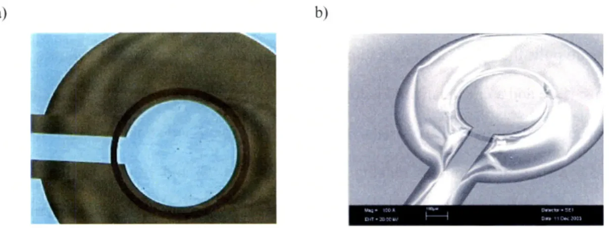
Figure 2.13. a) A top view of the center capacitor area taken from a microscope and b) a micrograph of the same device taken from SEM...55
Figure 2.14. Circuit model of anodic bonding silicon to glass with oxide as intermediate layer...58
Figure 2.15. Cross-sectional schematic of the device after wafer-level bond. ... 62
Figure 2.16. Surface profiles and cross-sections for a wafer-level bonded device...64
Figure 2.17. Cross-sections of the tunable capacitor as fabricated showing a), the device area and b) the fulcrum area... 64
Figure 2.18. Die-level anodic bond setup. ... 66
Figure 2.19. Surface profiles of the plate after die-level bond... 67
Figure 2.20. Cross section schematic of the clamped device...68
Figure 2.21. Schematic of the first package... 69
Figure 2.22. Schematic of the second package. ... 70
Figure 2.23. a), the assembled chip enclosed in the plastic housing, and b), the plastic housing is sandwiched between two PCB's with BNC connectors. ... 70
Figure 2.24. Picture of the new package ... 71
Figure 3.1. Simplified cross-sectional schematic of the actuator structure showing the three regions used in M atlab m odeling. ... 75
Figure 3.2. Simplified schematic of the actuator structure. ... 76
Figure 3.3. Boundary conditions of the outer membrane for the three cases a) before pull-in, b) zip-in and c) release. ... 78
Figure 3.4. Boundary conditions for a) the cylindrical fulcrum and b) the center plate...80
Figure 3.5. Simulation results for the plate and fulcrum before pull-in...89
Figure 3.6. Simulation results for the zip-in case...91
Figure 3.7. Simulation results for the release case... 92
Figure 3.8. MOS structure analysis showing a) depletion thickness and b) surface potential of sili-con as function of applied voltage ... 94
Figure 3.9. Flow chart of the data flow algorithm of the ESSOLV macro (ANSYS manual, Chapter
2, coupled-field guide)... 96
Figure 3.10. Schematic of the actuator used in FEM model...97
Figure 3.11. Deflection profiles of silicon plate for different sweep voltages...99
Figure 3.12. The end deflection of the plate as function of sweeping voltage comparing Matlab to A N S Y S . ... 100
Figure 3.13. Center deflection of plate after zip-in comparing Matlab to ANSYS. ... 101
Figure 3.14. Electrostatic hysteresis of the zipping actuator. ... 102
Figure 3.15. Deflection profile of the plate simulated with an applied voltage of 160 V...104
Figure 3.16. Zoomed-in plot of the deflection from 1350 to 1500 mm...104
Figure 3.17. Plots of the radial strain vs. plate thickness for radius r = 1700, 1650, 1600 and 1550 m m ... 10 6 Figure 3.18. Plots of the radial strain vs. plate thickness for radius r = 1500, 1460, 1420 and 1350 m m ... 10 7 Figure 3.19. Capacitance change of the a) capacitor and b) actuator as actuation voltage sweeps up and dow n ... 109
Figure 3.20. ANSYS model used in capacitance simulation. ... 110
Figure 3.21. The effect of fulcrum thickness on a) pull-in voltage and b) the moment transmission ratio and c) center deflection. ... 111
Figure 3.22. The effect of air gap on a) the pull-in voltage and b) the center deflection. ... 112
Figure 3.23. The combining effect of fulcrum thickness and air gap thickness for a) pull-in voltage and b) center displacement for two different plate thickness at a pin-down position of 1750 m m ... 113
Figure 3.24. The effect of fulcrum thickness and gap thickness on a) pin-down position and b) cen-ter displacement at two different plate thickness using 40V...114
Figure 3.25. Design of the plate with slits cut at the outer plate...116
Figure 4.1. Schem atic of the test setup. ... 120
Figure 4.2. a) Magnitude and b) phase plots of the center capacitor comparing the measurement to a series L C R m odel...122
Figure 4.3. Capacitance model of the device...123
Figure 4.4. Sim plified m odel. ... 123
Figure 4.5. Schematic of the optical probe. (source: ZMI optical probe accessory manual OMP-023 8B ) ... 125
Figure 4.6. Exploded view of the original design for the probe fixture...126 Figure 4.7. Schematic of the laser interferometer experiment set up...127 Figure 4.8. Picture of the test setup with the new package...129 Figure 4.9. Capacitance of the capacitor measured by HP 4294A as bias voltage scans from -40 V
to 40 V, then 0, and then 40 V to - 40 V twice, compared with measurement by HP
42 84A . ... 13 1
Figure 4.10. The actual geometry of the capacitor as predicted by the Wyko image and initial ca-pacitance. ... 132
Figure 4.11. Capacitance of the actuator measured by HP 4294A as bias voltage scans from 40 V to -40 V, then 0, and then -40 V to 40 V, and repeat to -40 V again...133 Figure 4.12. Displacement of the plate center measured using the laser interferometer as bias
volt-age is applied to the CAP and GND terminals for two tests...135 Figure 4.13. Capacitance change and center displacement when bias voltage is applied between the
CAP and GND terminals; the thicker lines are for test I in Figure 4.12 and the thinner
lines are for test 2...136 Figure 4.14. Displacement of the plate center measured using the laser interferometer as bias
volt-age is applied to the ACT and GND terminals for two tests. ... 137
Figure 4.15. Capacitance change and center displacement when external voltage is applied between the ACT and GND terminals. In the plot, test 1 and test 2 as shown in Figure 4.14 are plotted the sam e color...138 Figure 4.16. SEM photo of the cross-section showing the actual profile of the fulcrum. ... 139
Figure 4.17. The factors that are considered in the ANSYS model for the wafer-level-bonded
de-v ice...13 9
Figure 4.18. Deflection of the plate of device 9_1 using the Wyko interferometer showing a) 3-D im age and b) a cross-section...141 Figure 4.19. Profile of the plate at a cross-section after translation...142 Figure 4.20. A cross-section of the plate as fabricated comparing the Wyko measurement to
AN-SY S sim ulation...143
Figure 4.21. Center displacement of the plate vs. actuation voltage comparing laser experiments to various AN SY S sim ulations...144 Figure 4.22. Center displacement of the plate predicted by ANSYS...145 Figure 4.23. Capacitance of the actuator as bias voltage is applied to actuator of the
die-level-bond-ed device. ... 14 6
Figure 5.1. A design of the new electrostatic actuator...154
Figure 5.2. Axisymmetric 2-D equivalent model of the new actuator design. ... 154
Figure 5.3. The deflection profile of the plate with the new design using ANSYS...155
Figure 5.4. A 2-D cross section of the conceptual LC tank...156
Figure 5.5. Simplified schematic of the LC resonator. ... 156
Figure 5.6. Lumped parameter model of the LC tank...158
Figure 5.7. Magnitude response as capacitance is tuned from its initial value (the curve to the left) to the final value (the curve to the right). ... 160
Figure 5.8. Fabrication process of the new LC cavity resonator. ... 162
List of Tables
Table 3.1. Dimensions used in design and modeling...75
Table 3.2. Boundary conditions for the actuator, fulcrum and center plate after normalization. ...84
Table 3.3. Boundary functions used in Matlab BVP4C for the three stages a) before pull-in, b) zip-in and c) release ... 86
Table 3.4. Dim ensions used in the m ask layout...115
Table 5.1. Dimensions used in the simulation of the new actuator design...154
Table 5.2. Dimensions used and parameters derived in the Matlab simulation...159
Table A. 1. Dimensions and the designs used for each device in the mask layout. All dimensions are in m m . ... 170
Nomenclature
Greek
J9
a constant for the fulcrum 3 axial deflection of the fulcrum£ permittivity of air
COX permittivity of oxide 0 phase of the impedance
A wavelength of the laser measurement beam
p sheet resistivity of silicon
UA u electrical conductivity of gold
'7Si electrical conductivity of silicon
PO vacuum permeability
v Poisson ratio
normalized value
0 rotation at the joint between the fulcrum and the plate
to frequency
co0 resonant frequency
Roman
a inner radius of the actuator
A normalized value
b outer radius of the actuator
c thickness of the oxide insulator
C capacitance
C1 capacitance between the silicon plate and the central capacitor metal surface
C2 2 capacitance between the silicon plate and the actuator metal surface
C12 mutual capacitance between the capacitor and actuator metal surfaces
Ccap measured capacitance between the CAP and GND terminals
Cact measured capacitance between the ACT and GND terminals
C, final capacitance
Cg initial capacitance
COX capacitance across the oxide layer during anodic bond
CP I parasitic capacitance between the actuator metal surface and all other sur-faces except the actuator metal surface
Cp2 parasitic capacitance between the actuator metal surface and all other sur-faces except the capacitor metal surface
Cscr capacitance across the space charge layer
d depth of the cavity resonator
D flexural rigidity of the plate
Df flexural rigidity of the fulcrum
E young's modulus of silicon
f
frequency-fo resonant frequency
F electrostatic force
F, the nominal vacuum wavelength of one polarized laser beam
F2 the nominal vacuum wavelength of the other polarized laser beam
g initial air gap of the actuator
h thickness of the top plate
L inductance
I current
m width of metal interconnect
M, bending moment per unit length acting at the joint by the outer plate
M2 bending moment per unit length acting at the joint by the fulcrum
M3 bending moment per unit length acting at the joint by the center plate
Mr radial bending moment per unit length of the plate
Mt tangential bending moment per unit length of the plate
MX bending moment per unit length of the fulcrum of a section perpendicular to the x axis.
Mq, bending moment per unit length of the fulcrum of an axial section
p displacement measured by the laser interferometer
Q
shear force per unit length of the plateQ
quality factorr radius of the plate
ro outer radius of the bottom electrode
R normalized radius of the outer plate, also series resistance
R 'normalized radius of the center plate
R, radius of capacitor
R2 radius of toroid
Rc resistance of capacitance
RL resistance of toroid
Rglass resistance across the glass wafer
ROX leakage current resistance during anodic bond
Rscr leakage current across the space charge layer
ra radius of the fulcrum
rc radius of the capacitor
s radial pin-down position of the plate after zip-in
t thickness of the fulcrum
V actuation voltage
w vertical displacement of the plate
W normalized vertical displacement of the plate
WAit skin depth of gold
x axial coordinate of the fulcrum
X normalized axial coordinate of the fulcrum
y radial deflection of the fulcrum
Y normalized radial deflection of the fulcrum z vertical deflection of the center plate
Z normalized vertical deflection of the center plate
magnitude of the impedance ACT BOE BOX BVP CAP DI DRIE FEM GND LC LPCVD MEMS MOS MTL MTR ODE PCB PECVD PSI RF SEM SO' STS UWB VCO Iz Acronyms
the terminal that connects to the bottom electrode of the actuator buffered oxide etch (HF)
buried oxide
boundary value problem
the terminal that connects to the bottom electrode of the capacitor deionized water
deep reactive ion etch finite element analysis
the terminal that connects to the silicon plate inductor-capacitor
low pressure chemical vapor deposition micro-electro-mechanical system metal-on-semiconductor structure
microsystems technology laboratories at MIT maximum tuning ratio
ordinary differential equation printed circuit board
plasma enhanced chemical vapor deposition phase-shifting interferometry for the Wyko system radio frequency
scanning electron microscopy silicon on insulator
deep reactive ion etcher from Silicon Technology Limit ultra wide band communication
voltage controlled oscillator
VSI vertical-scanning interferometry for the Wyko system
ZMI Zygo motion interferometer system
Chapter
1
Introduction
In this thesis, design, fabrication, modeling and testing of a proof-of-concept MEMS tun-able capacitor are presented. The capacitor, together with a separate project on an exter-nally actuated, tunable cavity resonator, is origiexter-nally a joint effort in the development of a
MEMS tunable electromagnetic cavity resonator. The idea of such a cavity resonator is
inspired by the Nanogate and the electrostatic ziping-actuated micro relay, two devices that have been developed in our group. In this chapter, we will first elaborate on our inspi-rations for a cavity resonator and motivations for developing the tunable capacitor. And then literature research on tunable capacitor as well as resonators will be presented.
1.1 The Nanogate
The concept of implementing a tunable capacitor with circular zipping actuation traces back to a micro fluidic valve developed by J. White in our group [1]. The structure of the valve is dubbed "the Nanogate." It is a silicon-based MEMS device capable of nanometer-scale control over separation of two mm-nanometer-scale polished surfaces. The separation between the surfaces can range from contact to several microns, controllable with nanometer reso-lution.
Chapter 1: Introduction
The function of the Nanogate can be illustrated by the two cross-sectional schematics as shown in Figure 1.1. In the figures, the axis of revolution is through the center of the device. The device comprises a circular silicon diaphragm that is supported by a circular fulcrum as shown in Figure 1.1 a). The fulcrum acts as the torsional spring and allows the diaghragm to bend when a deflection is applied on the periphery by an external piezoelec-tric servo actuator, as shown in Figure 1.1 b). The center boss is hence lifted away from the glass base, creating a fluidic path. The device is fabricated by anodically bonding an etched silicon wafer to a Pyrex glass substrate. The lever-fulcrum action of the structure allows precise control of the gap opening. The opening and closing motion of the Nan-ogate has been measured in increments as small as 2.4 nm, the resolution of the laser mea-surement unit [2]. A capacitor sensor that measures the gap separation by detecting the capacitance change has also been developed in the group [3].
a) b)
No Appied DeNcion ScnApplied
DeDnon
rOe hasparke dtheh u -aon Periphery
Silicon Diaphs n zPpezpsleglrac Semo Silicon Diaphgrat
Torsion Spring ao rdin Sprg
Pyrx 7740 Base Par wit e
Oplical Probe ~ 5mm
Innteewwroriet4-Figure 1. 1. Operation principle of the Nanogate showing a) undeflected mode and b) deflected mode. (Courtesy of J. White)
The observation that the high-aspect-ratio gap of the Nanogate can be precisely con-trolled has sparked the idea of a high tuning-ratio capacitor. A laterally-moving electro-static zipping actuator using two opposing actuation surfaces etched with deep reactive ion etching techniques designed to actuate a micro relay was also developed in our group [4]. Combining these two ideas, a tunable capacitor with embedded actuator becomes a
Section 1.2: Electrostatic zipping actuator for a tunable capacitor
solid concept. In the next section, we will explain how the device could be transformed from a micro fluidic valve to a tunable electronic device.
1.2 Electrostatic zipping actuator for a tunable capacitor
The Nanogate valve uses an external piezoelectric actuator to apply a deflection to the periphery of the circular lever. While this is acceptable for a valve which will be installed in a much larger system, an external actuator will not be practical for a tunable capacitor that will be used inside a wireless transceiver, for example. If the actuator can be embed-ded into the device, lots of space can be saved. This can be best done by using the silicon diaphragm as an electrostatic zipping actuator.
It follows that we can design a capacitor that is formed by two smooth surfaces ini-tially separated by a dielectric layer. It can be tuned by applying voltage to a zipping actu-ator that is electrically isolated from the capacitor. The actuation causes one capacitor surface to pry apart from the other and controls the gap between the surfaces in the nanometer range. Furthermore, it is possible to integrate an inductor within the device to form an integrated LC tank. A preliminary concept is shown in Figure 2, where a variable capacitor is located at the center of the device. A single-turn inductor is embedded in the lever-fulcrum structure. The inductor operates as a resonant cavity, with a
Q
on the order of a hundred.Electrostatic Zipper 8C
Variable Nn
-Capacitor inuOtr
Figure 1.2. Schematic of the conceptual design of the tunable LC tank. (Courtesy of J. White).
The concept of an integrated, electrostatically actuated tunable capacitor and that of an electromagnetic resonator tuned by external piezoelectric transducer are being studied independently. In this thesis, only the tunable capacitor will be presented. We will intro-duce briefly the work of the resonator using a single-turn, toroidal inductor by another col-league. In the following sections, we will explore the applications for a tunable capacitor and a tunable LC tank or resonator.
1.3 Magnetically Coupled Electromagnetic Cavity Resonator
The quasistatic electromagnetic cavity resonator consists a parallel-plate capacitor sur-rounded by a single-turn, toroidal inductor. It is fabricated using processes such as KOH etch, shallow reactive ion etch, sputtered gold metallization and thermal compression
wafer bonding [5].
Figure 1.3 shows a cross-sectional view of the concept of the cavity resonator. The tor-oidal cavity is formed by joining two KOH-etched wafers using thermal compression bonding of gold surfaces. Gold covers the entire the cavity for high-Q operation. The cen-ter capacitor plates are pushed to close the gap by an excen-ternal piezoelectric transducer. Experiments showed that the resonator exhibited
Q
ranged from 110 to 240 with a fre-quency tuning range from 2.5 GHz to 4.0 GHz. However, because the current design uses a wire loop to magnetically couple the EM field in the cavity, it requires a delicate pick-and-drop process, which limits the practicality of the design. What can be done to improve the function of the device include 1) use electrical coupling to the capacitor instead of magnetic coupling through wire loop and 2) incorporate an integrated tunable capacitor to replace the external transducer.Chapter 1: Introduction 26
Section 1.4: Tunable capacitor 27
SI
Figure 1.3. Cross-sectional schematic of the cavity resonator with magnetic coupling [5].
1.4 Tunable capacitor
A tunable capacitor (or varactor) is a widely used component in transceiver circuits for RF
communication devices. Its applications include low noise amplifiers, band pass filters, voltage-controlled oscillators (VCO), etc. Traditional solid-state varactors are made with p-n or Schottky-barrier junction types of semiconductor structures. A voltage bias applied to the p-n or Schottky diodes modifies the charge in the junction and hence changes the junction capacitance. These kinds of solid-state varactors, however, have large losses and a low tuning range (typically 30% or less), which are often the limiting factors in RF cir-cuit design [6]. As the RF electronics consumer market continues to grow, there is a clear demand for new generations of consumer electronics to operate over a wide variety of Internet Protocol networks and standards, and as a result, they must possess multimode, multiband capabilities [7]. One solution that could make a frequency-hopping transceiver design a reality is to develop a new generation of tunable capacitors that have a large tun-ing ratio, high quality factor, linear response to RF power, low power consumption, and occupy a small space. Tunable capacitors fabricated with MEMS technology have shown
28Ch te1:Itouto many merits in this respect.
MEMS tunable capacitors are mechanical devices that use various actuation methods,
such as electrostatic or thermal actuation, to physically move the position of the plates or the dielectric constituents of a capacitor. For a parallel plate type of capacitor, if we define the plate area as A, the gap between the plates as g, and the permittivity of the media between the plates as c, then the capacitance is expressed as,
C6A c~s- (1.1)
g
If we define the unbiased capacitance as c,, and the capacitance after tuning as c,,
then the tuning range is defined as [6],
C-C C (1.2)
C, C,
and MTR is the maximum tuning range that can be achieved with the tuning capacitor. Another commonly used measure of capacitance change is the capacitance ratio, which is defined as the ratio of Cf: C;.
For a resonator with an inductor L and a capacitor C in series or in parallel, the reso-nant frequency is coo -- L. If we would use this resonator for the application of Ultra
Wide Band (UWB) communication, which requires tuning from 3.1-10.6 GHz with a 500 MHz band, we would need a tuning range of the capacitance that exceeds 11. Such a tun-ing range is impossible with solid-state varactors, but within reach ustun-ing MEMS technolo-gies. However, the figures of merits of a tunable capacitor include more than simply the tuning range. The Quality factor
Q,
which determines the loss of power in the device, isChapter 1: Introduction
Section 1.4: Tunable capacitor
critical to the performance of any band pass filter or VCO.
Q
is directly related to the par-asitic resistance R in the circuit for series and parallel LC resonators respectively,Qseries = (1.3)
o),, R C
QPar,le, = w, R C (1.4)
Furthermore, it is also desirable for the capacitor to attain linear response or remain constant to RF power. In summary, it is important to evaluate the overall system perfor-mance when designing a tunable capacitor component.
Reports on MEMS tunable capacitors with tuning range greater than the traditional solid-state varactors have proliferated in recent years. A few of the papers also demon-strated the system performance of tunable filters or VCO's using MEMS tunable capaci-tors. Tunable capacitors can be roughly grouped into two types, analog-tuned and digital-tuned. Three different technologies are identified so far for building these capacitors: based on parallel-plate approach (by changing the vertical gap), interdigital design (by changing the horizontal gap), and fixed capacitor with switch (digital) type [8].
1.4.1 Analog-Tuned Capacitors
We will show examples of analog-tuned capacitors and summarize the findings of part of the vast amount of literature available on this topic using a chart.
Young & Boser reported an electrostatic-actuated analog-tuned capacitor with two parallel plates as shown in Figure 1.4 [9]. The actuation voltage was 5 V but a tuning range of only 16% was achieved. They later integrated the capacitor and an off-chip inductor and demonstrated a functional VCO with frequency tunable from 707 to 721 MHz [10]. Dec & Suyama reported a three-plate analog-tuned capacitor with 2-4 V actua-tion voltage and a tuning range of 1.87 [11]. The schematic of the capacitor is shown in 29
Figure 1.5. The VCO circuit built using this capacitor and a spiral inductor achieved a quality factor of about 20 at 1-2 GHz [12].
Figre abe aacti S..parrpte g T r Fi. plate tspaitg
AIR - 0 _ _ _ PhClweskst k/ x'Ikt2
byAL &+ Bose. YId, D c &+uaa
HungaLda si uaio(nFsa edpplat fe
Sw~Fixed
Fxdplate
Figure 1.4. Parallel plate tunable capacitor Figure 1.5. Three-plate tunable capacitor by
by Young & Boser. Dec & Suyamna.
Hung and Senturia conducted simulation and shape-optimization for an electrostatic zipping-actuated tunable capacitor [13]. A cantilever type zipper actuator is used and capacitance tuning is achieved in the zipping regime, as shown in Figure 1.6. By chang-ing the shape of the bottom electrode, it is shown that optimized performance of the capac-itance, such as linear C-V characteristics, or linear f-V characteristics, can be achieved. Hung reported an automated procedure for simulation, optimization and layout for the design of the bottom electrodes. The simulation was done using a finite-difference approx-imation. Using his method, the layouts for the bottom electrodes for three different optimi-zation criteria are shown in Figure 1.7. The simulated performance is plotted in Figure 1.8.
A chart is used to summarize the published tuning capacitors as shown in Figure 1.9.
The maximum and minimum capacitances for analog-tuning capacitors are plotted against maximum actuation voltage, comparing the different actuation method.
Section 1.4: Tunable capacitor 31
Cantilever Botttom conductor
Insulator
(a) Cantilever bending (before pull-in)
(b) Cantilever tip pull-in
Zipping motion
(c) Zipping regime
Figure 1.6. Zipper actuator operation with increasing voltage.
17[A1iTA1FEFI
(a) (b)
[iLi7~HI
(c)
Figure 1.7. The shapes of the optimized bottom electrode for (a) linear C-V characteristics,
(b) linear f-V, and (c) maximum tuning range.
31
Chapter 1: Introduction 2 1.8 1.6 1,4 12 08 0.6 0.4 0.2 (a) 2.5 3 G U. 3.5 1200 1150 1100 1050 - 1000-950 900~ 850 800-750 700 1.5 2 2.5 Bias voltage (V) (b)
Figure 1.8. Simulation results of the tunable capacitor using the shapes in Figure 1.7, showing (a) C-V and (b) f-V characteristics.
14 -- -- --- - --- -- ---
--- --- -- --- -- -- ----
-- ----
-- --
--- --
---T
b Drve Ac ationZipping Ac ation-MUMP's liel P Gap Desi
10 2 30 40 10 60
Canti
70 80 Actuation Votlage (V)
Figure 1.9. Summary of published analog-tuning capacitors [14]-[25].
32
--- Linear C-V
--+-- Linear frequency
- Maximize tuning range
U C C) 0 0.5 1 1.5 2 Bias voltage (V) Linear C-V --Linear frequency k
&Maximize tuning range
A-A 3 3.5 12-10 8 0. 0 0. 6 -4 2 0 0 I I
Section 1.4: Tunable capacitor
1.4.2 Digital-Tuned Capacitors
We will also show examples of digital-tuned capacitors and compare them with the ana-log-tuned capacitors.
Goldsmith et al from Raytheon Systems Corporation reported an RF MEMS variable capacitor with a 22:1 tuning range with digital capacitance selection, using bistable
MEMS membrane capacitors with individual tuning ranges of 70:1 to 100:1 [26]. A
cross-section of the individual capacitor in both actuated and unactuated states is shown in Fig-ure 1.10. The substrate is high resistivity silicon substrates (>10 kQ cm) to reduce para-sitic loss. The buffer layer is a 1 pm thick silicon oxide layer. The bottom electrode is a layer of refractory metal less than 0.5 tm thick to provide good conductivity as well as smooth contact surface. The interconnects are 4 tm thick aluminum and the membrane is a thin aluminum layer less than 0.5 pm thick for good conductivity and mechanical prop-erties. A top view of the capacitor is shown in Figure 1.11. The capacitor has a ratio of on-state to off-on-state capacitance range from 70:1 to 100:1, a pull-in voltage range from 30 to
55 V, and a switch time range from 3 to 6 ps.
MetallIc M ran Top View
Thick Metal
Diewo Lw Electrode Membrane
Undercut Access SIgnu Holes Electrode Dielectric IN
Figure 1.10. The Goldsmith bistable capaci- Figure 1.11. Top view of the fabricated
tor. capacitor.
A varactor is constructed using these switchable MEMS capacitors as the control
ele-ment. The configuration for a 6-bit varactor is shown in Figure 1.12. Each bit contains one 33
Chapter 1: Introduction
or more MEMS capacitors in series with a fixed capacitor, which is used to yield the desired capacitance for each bit. In this example, the bits contain 16, 8, 4, 2, 1 and 0.5 pF of capacitances. Each capacitor is actuated by a control voltage, which is decoupled from the RF signal through a 5 kW thin-film resistor. The capacitance of the varactor ranges from 1.5 pF with none of the bits actuated to 33.2 pF with all of the bits actuated. And a linear capacitance response in between these two values is obtained. The quality factor of the varactor is less than 20 at 1 GHz. The same group later demonstrated a 4-bit capacitor for 6 pole tunable filter using the same technology [27]. Goldsmith's example showed one of the early efforts in achieving desired capacitance characteristics by optimizing the cir-cuit design. However, a high actuation voltage and low quality factor were the limiting factors for wider applications of the bistable membrane capacitor.
keauphig Figure 1. 12. Configuration of GA Pr 4A PF I-74 p :F~p DC
the variable capacitor using individual MEMS capacitors.
Rizk and Rebeiz reported a digital type RF MEMS switched capacitor built in a CPW
configuration [28]. A 2-bit capacitor array is constructed using the switched capacitors. In
Secton .4: unale cpactor35
this design, a MEMS shunt bridge is fabricated over an MIM capacitor that allows for high capacitance ratio and also ensures a fixed down-state capacitance. A cross section of the switched capacitor is shown in Figure 5. Here the substrate is a 400-pm thick high-resis-tivity silicon wafer (2-3 kn cm). The pull-down electrodes are 0.6 pm thick layer of Ti/ Au/Ti layers. The dielectric is 0.2 pm thick silicon nitride. The MEMS bridge is fabricated using a 0.8 pm thick sputtered layer of gold using PMMA as sacrificial layer. The center conductor, the ground planes and the anchors are electroplated with 2 pm of gold. A
2-bit digital capacitor array is constructed using 300 fF and 600 fF switched capacitors. An equivalent circuit model is shown in Figure 6. The array is suitable for a digital tunable matching network at 0.5-3 GHz.
Z. ,
Bump MIM capacitor
MEMS bridge ,,Cl ,C
Figure 1.13. Cross section of the CPW shunt MEMS Figure 1.14. 2-bit circuit model.
switched capacitor.
Hoivik et al. reported a digitally controllable variable capacitor [29]. In this case, electrostatic actuation is used for analog tuning of the capacitor. Individual capacitor plates are connected to the bond pads using beam flexures of different widths as shown in Figure 1.15. As applied voltage is increasing, the top capacitor plates move towards the substrate in a cascading manner depending on the stiffness of the individual support beam. The device is fabricated using MUMPs technology. It includes three layers of polysilicon, two layers of oxide and one layer of gold. A plot of the capacitance ratio vs. voltage is shown in Figure 1.16.
Chapter 1: Introduction
Capacitance raft v& Vo~, 4.5 . 4 - . 3 25 -2 0.0 5.0 10.0 15.0 20.0 25.0 30.0 35 voltage Bottom Electrod
Figure 1.15. Top and cross-sectional view of the capacitor.
Figure 1.16. Capacitance ratio vs. Voltage.
In general, analog-tuned capacitors use lower actuation voltage and allow continuous frequency tuning; however, they possess lower tuning ranges than digital-tuned capaci-tors. On the other hand, digital-tuned capacitors have lower quality factors, and a lot of research effort will still be needed in achieving the desired frequency characteristics.
1.5 Integrated LC Resonator
Although a lot of work has been done to improve the performance of tunable capacitor with either analog- or digital-tuned functions, few paper reports on integrated LC resona-tor on a chip. This is because on-chip spiral type of inducresona-tors are often very lossy due to large resistance resulted from long spiral wires. Ketterl et al. reported a micromachined tunable CPW resonator which consists of a CPW spiral inductor with an electrostatic
zip-36
Individual plates snapping down
Section 1.6: Summary 37
ping cantilever type tunable capacitor [30]. Frequency tuning between 3 and 7 GHz was achieved with 40 V actuation voltage. However, the quality factor was between 17 and 20. There is a demand for a high-Q, highly tunably LC tank, conceivably in the wireless com-munication applications.
Portable wireless communication transceivers today continue to rely on off-chip reso-nator components (e.g., Surface Acoustic Wave, or SAW, filters) for high frequency selec-tivity and low noise performance. However, these off-chip passive components often occupy substantial space and consume substantial power. In a RF front end receiver, for example, a voltage controlled oscillator (VCO) generates a design frequency that upon mixing with the pre-filtered and amplified incoming radio signal, down converts the high frequency carrier signal to intermediate frequency (IF) before further signal processing. Currently, this is commonly done using off-chip LC tanks, and a charge-pump PLL (phase lock loop) implemented with an off-chip crystal frequency reference is needed in order to control the frequency and reduce phase noise. There could be substantial advantage in replacing the off-chip LC tank with IC-integrated on-chip LC tank in terms of space and power consumption. It is foreseeable that the RF transceiver architecture we use today will have to be re-designed to maximize the use of micromechanical circuits, e.g., MEMS var-actors, switches and resonators, etc. [31]. A lot of research is also being done on microme-chanical resonators, which possess exceptionally high Q and thermal stability, but often with very low tunability.
1.6 Summary
In this chapter, we have explained the enabling technologies for the concept of a tunable
LC tank, which are the Nanogate structure and the zipping actuator developed in our
group. The idea of the LC tank prompted separate studies on the single-turn inductor and
the tunable capacitor with integrated actuator. This thesis presents the study on the tunable capacitor. The chapter also provides an overview for the application of tunable capacitors and compares the many reported tunable capacitors in the literature, which can be grouped into several actuation methods in general. Our design of the tunable capacitor takes a rather different approach compared to the literature, because it is designed to be an inte-grated part of a cavity resonator. Lastly, we show that there is potential application for an integrated LC tank in the future wireless transceiver design.
1.7 Thesis Organization
We will start the thesis work by a chapter on design and fabrication. This is not because they proceed modeling, rather, the design, fabrication and modeling processes for a MEMS device are often entangled and there is no exception here. However, in particular to this thesis work, the reader should keep in mind that it is initially enabled by known technologies or designs, although it is driven by applications as well. Therefore, an intro-duction to the design and fabrication of the device will give a good overview on why the specific design is chosen and why we think we can make it. Having such knowledge would be essential to the understanding of the modeling and simulation, which is intro-duced the next. We will then present the testing of the device and compare the test results with the simulation results. The goal is to understand the function of the designed tunable capacitor, and from there, propose improved design schemes for an integrated cavity reso-nator, which will be described in the last chapter.
Chapter 1: Introduction 38
Chapter
2
Design and Fabrication
We have mentioned about the design concept of the tunable capacitor in the previous chapter. In this chapter, we will put the concept into a solid design and describe the micro-fabrication process that supports the design. The actual micro-fabrication process, like with any other MEMS device, is an iteration process where both design and fabrication have to compromise until they find an agreement. We will present the fabrication results and describe some important fabrication issues and how they are resolved. The assembly and packaging methods will be presented last.
2.1 Design
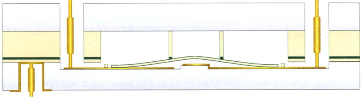
Based on the ideas of the Nanogate and the zipping actuator described in the previous chapter, a design of the electrostatically actuated tunable capacitor is devised. A cross-sec-tional schematic of the original design is illustrated in Figure 2.1. A 3-D bisected sche-matic of the device is shown in Figure 2.2. We will first briefly describe the structure of the device as well as its functions by referring to these two schematics.
40 Chapter 2: Design and Fabrication
Actuator Electrode Zipping Actuator Oxide Insulator Fulcrum Capacitor Electrode
Glass Wafer Sol Wafer Glass
Two Grounded Electrodes for Bottom Gold Electrode Capacitor Top Metal Electrode Tethers Actuator and Capacitor With Oxide Insulator
Figure 2.1. Cross-sectional schematic of the design of the tunable capacitor (dimensions not to scale).
Pyrex Capacitor Fulcrum
Wafers SI Plate SO Wafer
Figure 2.2. 3-D bisected view of the tunable capacitor (dimensions not to scale).
As shown in Figure 2.1, the device consists of three wafers: a SOI (Silicon-On-Insula-tor) wafer sandwiched by two glass wafers that are anodically bonded together. In the cen-ter of the device is a circular plate that is supported by tethers that are connected to the outer walls. A cylindrical fulcrum, to be fabricated by the deep reactive ion etching tech-nique, acts as the pivot for the plate and divides the plate into the outer actuator region and the center capacitor region. The top of the fulcrum is bonded to the top glass wafer for structural rigidity. The SOI layer is used as the zipping actuator because of its uniform
thickness and the low stress of single-crystal silicon. Metal (aluminum) is deposited on the
SOI layer facing the bottom glass wafer as electrodes for both actuator and capacitor.
Sili-con dioxide is used as dielectric material and it can be deposited on top of the metal by chemical vapor deposition. The bottom wafer contains the bottom electrodes for the actu-ator and the capacitor. The actuactu-ator electrode is etched into the glass to form the gap of the actuator. Gold is deposited on top of the etched pit as actuator and capacitor electrodes. Voltage is applied between the top and the bottom actuator electrodes. At a certain voltage threshold, the outer plate snaps down. With increasing actuation voltages, the plate zips along the radial direction and results in the separation of the two capacitor surfaces. It is known that gold adheres to oxide poorly, making it necessary to use an adhesion layer such as chromium when depositing gold onto silicon or oxide surface [32]. With such property, the plate does not bond to the gold surface although the two surfaces are in close contact during operation. Thus the design makes it possible to have two initially closely-contacted surfaces that can be pried apart. By changing the gap between the two plates of the capacitor, the capacitance can be tuned.
The actual fabricated device, however, is a simpler version that is without the top metal electrode due to facilities and cost constraints, which will be explained in the next section.
2.2 Fabrication Process
The device uses 2 glass wafers and 1 silicon wafer that are anodically bonded together. The top and bottom wafers are 500-pm thick Pyrex® Borosilicate 7740 wafers from Com-ing Inc. The middle wafer is a SOI wafer that has 340 pm thick handle, 1.5 jpm thick bur-ied oxide and 10 or 20 ptm thick SOI layer. Both the handle and SOI are Boron doped with a resistivity of 5-18 mn cm.
A total of 7 chrome masks were used for the fabrication of the device although 9 were
designed. The wafer layout and all the masks used are shown in Appendix A, which also includes a list of the dimensions and different designs used in the layout. A detailed fabri-cation log can be found in Appendix B. Fabrifabri-cation steps for the three wafers are listed below, and fabrication results will be presented in the next section.
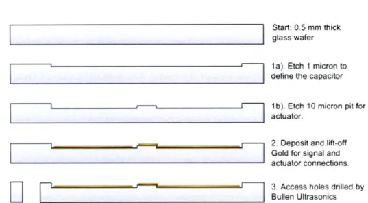
2.2.1 Top Wafer
The top glass wafer contains access holes for the electrodes that are 3.25 mm in diameter. The holes are drilled by Bullen Ultrasonics Inc., which creates cutting tools for the holes and uses ultrasonically-induced vibrations delivered to the tool to achieve microscopic grinding [33]. The process schematic is shown in Figure 2.3.
Start: 0.5 mm thick
glass wafer
D
. Drill holes forelectrode access by Bullen Ultrasonics
Figure 2.3. Process schematic for the top wafer.
2.2.2 Device Wafer
The middle wafer contains the structural plate that acts as the zipping actuator and the ful-crum that acts as the torsional spring. We will show the fabrication plan for the original design with metal. The schematic of the original fabrication process is shown in Figure 2.4, with fabrication steps followed.
Chapter 2: Design and Fabrication 42
Section 2.2: Fabrication Process 43
I
I
I
I
-Ii..u~1
Ii II
El
AD M
7g
a-Schematic of the fabrication
Start: S0l, 10/20 pm
Sol; 1.5 pm oxide, -340 pm handle 1. Thermal oxidation for 500 nm.
2. DRIE front side for the actuator for 10/20 um.
3. Target mount the front side to 4* wafer and DRIE back side for the fulcrum for -340 um in STS1. Dismount.
4. Strip surface oxide in BE.
5. Regrow thermal oxide.
6. E-beam aluminum using lift-off, or use a wafer shadow mask.
7. PECVD oxide for 300 nm.
Then plasma etch oxide.
steps for middle wafer.
1. Oxide was thermally grown under wet conditions at 1100 C for 0.5 p.m. This oxide
layer was used as a hard mask to protect the silicon surface for later anodic bonding after a deep reactive ion etch. After oxide growth, alignment marks were etched on the bottom side with mask 1: ALIGN, and the top side was etched with mask 2: STREETS, which partitioned the devices for die sawing. Both sides had alignment marks for aligning the wafers when bonding to the top and bottom glass wafers.
2. Deep reactive ion etch was used to etch the SOI layer to define the plate and tethers. The mask used was mask 3: ACTUATORTOP.
El
Figure 2.4.:1
L j
I:j
L:j
Chapter 2: Design and Fabrication
3. The wafer was mounted to 4" quartz wafer and deep reactive ion etch was used to
etch the fulcrum. The wafers were dismounted in oxygen plasma and then cleaned in pira-nha solution. Mask 4: FULCRUM.
4. All oxide on the surface was stripped in BOE, including the oxide grown in step 1 as well as the exposed buried oxide.
5. Then thermal oxide was grown again, covering the whole wafer for about 0.3 pim. This oxide layer insulates the metal from the rest of the silicon in the device.
6. To deposit aluminum on the top surface, lift-off using photoresist can be one option,
which involves spraying photoresist on top of the wafer surface since spin deposition is not possible. Another option is to use a wafer shadow mask placed on top of the wafer using drops of photoresist as adhesive. Then e-beam evaporation is used to deposit alumi-num. Mask 5: METALTOP.
7. PECVD oxide for 300 nm then etch oxide in plasma. Mask 6: OXIDE.
The actual fabrication process omitted steps 6 and 7 because of practical reasons that will be explained in the section followed.
2.2.3 Bottom Wafer
Fabrication of the bottom wafer is shown in Figure 2.5. Two batches of the bottom wafer were fabricated; one with the center capacitor etched for 1 ptm, and the other without the initial etch. The rest of the process was the same for the two batches and the general fabri-cation steps are as follow.
1. For one batch, a 1-pim deep circular pit was first etched in BOE to define the height
of the capacitor plate as in step I a) in the figure. Mask 7: CAPACITORSEAT was used. For another batch, step 1 a) was omitted. For both batches, a 10 pim pit was etched to define the gap of the actuator using mask 8: ACTUATORBOTTOM.
![Figure 1.3. Cross-sectional schematic of the cavity resonator with magnetic coupling [5].](https://thumb-eu.123doks.com/thumbv2/123doknet/14310551.495279/27.918.206.727.177.400/figure-cross-sectional-schematic-cavity-resonator-magnetic-coupling.webp)