HAL Id: hal-00453804
https://hal.archives-ouvertes.fr/hal-00453804v3
Submitted on 13 Jan 2011
HAL is a multi-disciplinary open access
archive for the deposit and dissemination of
sci-entific research documents, whether they are
pub-lished or not. The documents may come from
teaching and research institutions in France or
abroad, or from public or private research centers.
L’archive ouverte pluridisciplinaire HAL, est
destinée au dépôt et à la diffusion de documents
scientifiques de niveau recherche, publiés ou non,
émanant des établissements d’enseignement et de
recherche français ou étrangers, des laboratoires
publics ou privés.
Direct observation of Oersted-field-induced
magnetization dynamics in magnetic nanostripes
Vojtech Uhlir, Stefania Pizzini, Nicolas Rougemaille, Vincent Cros, Erika
Jimenez, Laurent Ranno, Olivier Fruchart, Michal Urbanek, Gilles Gaudin,
Julio Camarero, et al.
To cite this version:
Vojtech Uhlir, Stefania Pizzini, Nicolas Rougemaille, Vincent Cros, Erika Jimenez, et al.. Direct
observation of Oersted-field-induced magnetization dynamics in magnetic nanostripes. Physical
Re-view B: Condensed Matter and Materials Physics (1998-2015), American Physical Society, 2011, 83,
pp.020406. �10.1103/PhysRevB.83.020406�. �hal-00453804v3�
nanostripes
V. Uhl´ıˇr,1, 2 S. Pizzini,1 N. Rougemaille,1 V. Cros,3 E. Jim´enez,4 L. Ranno,1 O. Fruchart,1
M. Urb´anek,2 G. Gaudin,5 J. Camarero,4 C. Tieg,6 F. Sirotti,7 E. Wagner,1 and J. Vogel1, ∗
1
Institut N´eel, CNRS and UJF, BP166, 38042 Grenoble, France
2
Institute of Physical Engineering, Brno University of Technology, 61669 Brno, Czech Republic
3
Unit´e Mixte de Physique CNRS/Thales, Route d´epartementale 128, 91767 Palaiseau cedex, France
4
Dpto. F´ısica de la Materia Condensada, Instituto “Nicol´as Cabrera” and IMDEA-Nanociencia, Campus Universidad Aut´onoma de Madrid, 28049 Madrid, Spain
5
SPINTEC, UMR8191, CEA/CNRS/UJF/GINP, INAC, 38045 Grenoble, France
6
ESRF, BP200, 38043 Grenoble, France
7
Synchrotron SOLEIL, L’Orme des Merisiers, Saint-Aubin, 91192 Gif-sur-Yvette, France We have used time-resolved x-ray photoemission electron microscopy to investigate the magne-tization dynamics induced by nanosecond current pulses in NiFe/Cu/Co nanostripes. A large tilt of the NiFe magnetization in the direction transverse to the stripe is observed during the pulses. We show that this effect cannot be quantitatively understood from the amplitude of the Oersted field and the shape anisotropy. High frequency oscillations observed at the onset of the pulses are attributed to precessional motion of the NiFe magnetization about the effective field. We discuss the possible origins of the large magnetization tilt and the potential implications of the static and dynamic effects of the Oersted field on current-induced domain wall motion in such stripes.
The possibility to manipulate the magnetic configura-tion of nanostructures by using electrical currents is a recent, exciting development in spintronics. Electrical currents can affect the magnetization of magnetic nanos-tructures both through the charge and the spin of the conduction electrons. In recent years it has been shown that Spin-Transfer Torque (STT) [1, 2] and Rashba spin-orbit torque effects [3] act on the magnetization, in addi-tion to the classical Oersted magnetic field (HOe). In
gen-eral, the combination of these effects should be taken into account in the description of the magnetization dynamics during the application of a current pulse. For instance, it was shown that the contribution of the Oersted field and not only STT is needed to explain the magnetization reversal in trilayered pillars induced by a current flowing perpendicular to the plane of the layers [4, 5]. For in-plane currents, HOe has been invoked to explain
magne-tization reversal in mesoscopic NiFe/Cu/Co/Au bars [6] and the resonant depinning of constricted domain walls (DWs) in NiFe/Cu/Co trilayers [7].
Several studies of the effect of current pulses on the magnetization of nanostripes, mainly concerning current-induced domain wall motion (CIDM), have been based on the observation of the domain structure before and after the application of a current pulse [8, 9]. How-ever, the effect of the Oersted field on the magnetiza-tion can only be investigated by direct, dynamic ob-servations during the current pulses. This has been achieved in this work, using time-resolved x-ray mag-netic circular dichroism combined with photoemission electron microscopy (XMCD-PEEM). Our results show that the current-induced field during nanosecond pulses causes both quasi-static and precessional effects on the NiFe magnetization. These effects may contribute to the
increased efficiency of current-induced domain wall mo-tion observed in such trilayers [10–12].
Stacks of Cu(2nm)/Ni80Fe20(5nm)/Cu(5nm)/Co(5nm)/
CoO(6nm) deposited on highly resistive Si(100) (ρ > 300 Ω.cm) were patterned in 400 nm wide zigzag stripes, with angles of 90◦ and 13 µm long straight
sections, combining electron beam lithography and ion-beam etching. Contact electrodes made of Ti/Au were subsequently deposited using evaporation and a lift-off technique. Prior to the XMCD-PEEM measurements, most of the 2 nm Cu protective layer was removed in-situ using Ar-bombardment, to increase the XMCD signal of the NiFe layer.
XMCD-PEEM measurements were performed at the synchrotron SOLEIL (TEMPO beamline), using a Fo-cus IS-PEEM. The magnetic configuration in the NiFe layer was imaged by measuring the Ni XMCD intensity, tuning the x-ray energy to the Ni L3 absorption edge
(852.8 eV). To optimize the magnetic contrast, the dif-ference between two consecutive images obtained with 100% left- and right-circularly polarized x-rays was com-puted. For each circular polarization, 60 images of 0.5 s were summed, after correction for possible image drifts.
Temporal resolution was obtained by synchronizing nanosecond current pulses applied to the nanostripes with the SOLEIL 8-bunch mode, where photon bunches arrive at the sample with a repetition rate of 6.77 MHz. The temporal evolution of the magnetic configuration in the nanostripes was obtained by recording images for dif-ferent delays between the current and photon pulses [13– 16]. If events are reproducible and reversible for each cur-rent pulse, the temporal resolution of this pump-probe technique is limited only by the duration of the pho-ton pulses (50-60 ps). The total acquisition time of 1
2 minute for each XMCD-image implies that sequences of
about 4 × 10⁸current (pump) and photon (probe) pulses
were averaged. In order to avoid electrical discharges, the voltage between the sample and the objective lens of the PEEM was set to 5.4 keV instead of the nominal 12 keV, limiting the spatial resolution to about 0.6 µm.
Figure 1 shows a series of XMCD-PEEM images of the NiFe magnetization acquired during the application of bipolar current pulses [Fig. 1]. The positive/negative part of the pulse is about 2 ns/1 ns long, with a maxi-mum amplitude of +7 mA/−9 mA. The latter value cor-responds to a current density of 1.5 × 10¹² A/m2
as-suming a homogeneous current distribution in the stack. Before and after the current pulses, the magnetization is aligned along the stripe axis and no domain walls are present, leading to an almost homogeneous XMCD inten-sity [Fig. 1(a)]. During the current pulses, the NiFe mag-netization tilts away from the wire axis, with a tilt angle ϕt. This tilt is anti-clockwise for a positive and clockwise
for a negative current direction, as can be inferred from the magnetic contrast in the differently oriented sections of the nanowire [Figs. 1(d) and (g)]. The approximate magnetization directions in two of the wire sections are indicated before the current pulses (a), and at the end of the plateau of the positive (d) and negative part of the pulses (g). In (d) and (g) also the electron flow directions are indicated. The delays between the beginning of the current pulse and the photon pulses at which the images were acquired are shown in Fig. 1(i) [17].
In order to obtain the tilt angle ϕt as a function of
time during the current pulses [Fig. 1(i)], the normalized XMCD-intensity in the bends of the stripe was deter-mined from the XMCD-PEEM images. The XMCD in-tensity is proportional to the cosine of the angle between the incoming x-rays and the local magnetization, thus for the bends IXMCD∝M cos(ϕt) cos(α), where M is the
magnetization and α is the angle between the x-ray inci-dence direction and the sample surface. This angle is con-stant (25◦) and we also suppose the magnetization
vec-tor has a constant amplitude. No change of the magnetic contrast due to current-induced heating was observed. At zero current, the magnetization is parallel to the stripe axis and thus ϕt = 0◦, giving IXMCD = M cos(α) = I0.
Then ϕt can be determined from the different images by
ϕt= arccos(IXMCD/I0).
The NiFe magnetization tilt induced by the transverse Oersted field is surprisingly large, with a value of about 75◦ at the end of the positive part of the pulse. For a
soft magnetic material such as NiFe, the magnetization direction in a nanostripe is mainly determined by mag-netostatic effects, which favor magnetization along the stripe axis. For a 5 nm thick, 400 nm wide stripe the transverse demagnetizing factor is about 0.023 [18]. In a first approximation, this would mean that a transverse field of 0.023 × µ0MS×sin 75◦= 22 mT (with µ0MS = 1
T for permalloy) would be required to obtain ϕt= 75◦.
FIG. 1. (color online) Time-resolved XMCD-PEEM images of the NiFe layer of a 400 nm wide nanostripe at time delays of (a) 0 ns, (b) 0.35 ns, (c) 0.45 ns, (d) 1.9 ns, (e) 2.3 ns, (f) 2.4 ns, (g) 3.3 and (h) 3.6 ns with respect to the beginning of the positive part of the bipolar current pulse [17]. These delays are indicated on the bipolar pulse plotted in (i), together with the magnetization tilt angle ϕt. The oscillations in ϕt at
the beginning of the positive and negative parts of the pulse indicate magnetization precession about HOe.
The Oersted field inside a stripe with rectangular cross-section is given by Bx= µ0Jz, where J is the current
den-sity and z is the distance from the stripe axis. A current of +7 mA corresponds to a current density of 1.17 × 10¹²
A/m2, yielding an average field acting on the NiFe
mag-netization of HOe= 7.4 mT if we assume a homogeneous
current distribution over the NiFe/Cu/Co trilayer struc-ture, and 11 mT for a current flowing entirely through the Cu and Co layers. With a field of 11 mT, the expres-sion given above yields a ϕt of only 28◦ instead of the
observed 75◦.
The most likely origin of the discrepancy between the observed and expected tilt angles is an overestimation of demagnetizing effects. The value of ϕt = 28◦ is
obtained assuming that the tilt is homogeneous over the stripe width. In reality, the demagnetizing effect is much smaller in the center than at the edges of
the stripe, leading to a larger tilt angle in the cen-ter. We carried out micromagnetic simulations using the OOMMF code [19] to obtain the magnetization profile of a 400 nm wide, 5 nm thick layer of Ni80Fe20 and for
NiFe(5nm)/Cu(5nm)/Co(5nm) trilayers under an Oer-sted field of 7.4 mT. The results obtained for NiFe (Co) using an exchange constant A of 1×10⁻¹¹J/m (3×10⁻¹¹
J/m), a spontaneous magnetization µ0MS of 1T (1.76T)
and a vanishing magnetic anisotropy constant K, are shown in Fig. 2. The blue (black) continuous line shows the demagnetizing factor (ϕt) for a single Py layer, as a
function of transverse position. The average tilt angle is 26.6◦with a maximum of 32◦in the center of the stripe.
As shown by previous studies, edge roughness can lead to a decrease of the transverse demagnetizing factor of several tens of percent [20]. The simulated magnetiza-tion profile obtained by adding a random lateral rough-ness of 4-8 nm (1-2 grid cells) at the stripe edges (dotted black line) leads only to a slight increase of the average tilt angle (to about 30◦). Edge roughness is therefore
not sufficient to explain the large experimental tilt. A better quantitative agreement with experiments can be obtained by taking into account the presence of the Co layer. Magnetostatic interactions between the NiFe and Co layers can significantly decrease the transverse demag-netizing effects with respect to single NiFe wires. Part of the magnetic charges on the edges of the NiFe layer can be compensated by mirroring effects on the edges of the Co layer, as shown by micromagnetic simulations [21]. Moreover, if the current is centered in the Cu layer the Co magnetization tilt induced by HOewill be opposite to
the one induced in the NiFe layer, further increasing the compensating effect of the Co magnetic charges. The av-erage tilt angle obtained for the NiFe layer in the case of a NiFe/Cu/Co trilayer is around 69◦, close to the
exper-imental value, with a Co tilt angle (not shown) of about -42◦. The NiFe magnetization tilt strongly depends on
the Co tilt angle. In the simulations of Fig. 2, the mag-netic anisotropy in the Co layer was taken to be zero, which is justified by the polycrystalline nature of the Co leading to the absence of an in-plane uniaxial anisotropy before patterning. A uniaxial Co anisotropy along the stripe axis of 50 kJ/m3 would lead to a Co tilt angle of
only -9◦, and a NiFe tilt of 42◦.
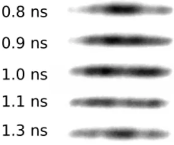
At the onset of the current pulse, fast oscillations of the magnetization are observed in the time-resolved im-ages [Fig. 1(i)]. These oscillations are due to the preces-sion of the magnetization about the effective field. Fig-ure 3 shows contrast-enhanced XMCD-PEEM images of the bottom section of the nanostripe of Fig. 1. Inho-mogeneities in the dipolar interactions with the Co layer and in edge roughness lead to inhomogeneous magnetic contrast in the sections of the spin-valve nanowire. Dif-ferent parts of the nanowire oscillate with difDif-ferent ini-tial phases of the precessional motion. The exchange interaction between the different parts, however, leads
0 50 100 150 200 250 300 350 400 0 10 20 30 40 50 60 70 80 90 0.00 0.05 0.10 0.15 0.20 0.25 0.30 T ilt a n g le ( d e g ) Transverse position (nm) D e m a g n e tiz in g fa c to r
FIG. 2. (color online) NiFe magnetization tilt angle as a function of the transverse position inside a 400 nm wide stripe, obtained using the OOMMF code, for a transverse Oersted magnetic field of 7.4 mT. The experimental NiFe tilt angle is indicated with a dashed line. Different cases were considered : a single, 5 nm thick NiFe layer without edge roughness (black), a 5 nm think NiFe with a random edge roughness of 4-8 nm (dotted black), and a NiFe(5nm)/Cu(5nm)/Co(5nm) trilayer (red). The demagnetization factor along the wire is also shown (blue, right y-axis)
to spatio-temporal variations of the magnetic contrast that resemble spin waves. The oscillatory and propaga-tive nature of these contrast variations is more clearly visible in the accompanying movie [17]. The excitation of spin-waves by the Oersted field in spin-valve trilay-ers was predicted by Kim et al. [22] and spin-wave-like features were observed using Lorentz microscopy on 30 nm thick NiFe nanostripes upon current injection [23]. Further micromagnetic simulations are necessary to un-derstand these oscillations quantitatively, but our results show that time-resolved XMCD-PEEM is a very suitable technique to observe such magnetization oscillations.
0.8 ns 0.9 ns 1.0 ns 1.1 ns 1.3 ns
FIG. 3. Time-resolved XMCD-PEEM images of the lower, 13 µm long section of the nanostripe, taken at the indicated delays after the beginning of the positive part of the current pulse. Spatio-temporal variations of the XMCD contrast at a frequency of about 2 GHz are visible [17].
In quasi-static measurements performed on similar nanostripes we have observed that current pulses with a density above 1.5 − 2 × 10¹²A/m2 can induce nucleation
of reversed domains in initially saturated nanostripe sec-tions [12]. Our present results suggest that the precession of the magnetization about HOe is possibly at the origin
4 of this local magnetization reversal, similar to the
mag-netization reversal [24] induced by transverse magnetic field pulses in magnetic nanostructures.
The magnetization tilt induced by the Oersted field and amplified by magnetostatic interactions should also have an influence on current-induced domain wall mo-tion in such trilayers [10–12]. The amplified Oersted field might stabilize transverse domain walls having their magnetization parallel to HOe, like it was observed for
field-induced domain wall motion in trilayer nanostripes in the presence of a transverse magnetic field [25, 26].
In conclusion, we provide direct, time-resolved micro-scopic evidence of the effect of current-induced fields on the magnetic configuration of magnetic nanostripes. We show that the combination of Oersted fields and strong dipolar interactions that may exist in nanostripes com-prised of several metallic layers produce and amplify a large tilt of the magnetization. The quasi-static and pre-cessional effects induced by the amplified Oersted field should be carefully considered when current pulses are applied to magnetic wires with different metallic layers, for instance to study current-induced domain wall mo-tion. On the other hand, the effect of the Oersted field on magnetization reversal or magnetic domain wall mo-tion in future spintronic devices can be tailored by tuning the thickness of the different metallic layers.
We acknowledge the invaluable technical and exper-imental help of P. Perrier, D. Lepoittevin, L. Del-rey, S. Pairis, T. Fournier, A. Hrabec, M. Bonfim and W. Wernsdorfer. We thank A. Anane, J. Grollier and R. Mattana for experimental help and useful discussions. We thank the European Synchrotron Radiation Facility (ESRF), and in particular the staff of beamline ID08, where several preliminary experiments were carried out. Nanofabrication was performed at the ‘Plateforme de Technologies Avanc´ees’ and at the Institut N´eel/CNRS ‘Nanofab’ facility, both in Grenoble. E.J. and J.C. ac-knowledge financial support through projects HF2007-0071, S2009/MAT-1726, and CSD 2007-00010. V.U. was financially supported by grants No. MSM0021630508, No. KAN400100701 and No. 2E13800101-MSMT, and by the project INGO No. LA287 of the Czech Ministry of Education. This work was partially supported by the ANR-07-NANO-034 ‘Dynawall’.
∗ jan.vogel@grenoble.cnrs.fr; http://neel.cnrs.fr/
spip.php?rubrique52&lang=en
[1] L. Berger, J. Appl. Phys. 55, 1954 (1984).
[2] J. Slonczewski, J. Magn. Magn. Mater. 159, L1 (1996). [3] I. M. Miron, G. Gaudin, S. Auffret, B. Rodmacq,
A. Schuhl, S. Pizzini, J. Vogel, and P. Gambardella, Na-ture Mater. 9, 230 (2010).
[4] Y. Acremann, J. P. Strachan, V. Chembrolu, S. D.
An-drews, T. Tyliszczak, J. A. Katine, M. J. Carey, B. M. Clemens, H. C. Siegmann, and J. St¨ohr, Phys. Rev. Lett. 96, 217202 (2006).
[5] K. Ito, T. Devolder, C. Chappert, M. J. Carey, and J. A. Katine, J. Phys. D - Appl. Phys. 40, 1261 (2007). [6] D. Morecroft, I.A. Colin, F.J. Casta˜no, J.A.C. Bland,
and C.A. Ross, Phys. Rev. B 76, 054449 (2007). [7] P.J. Metaxas, A. Anane, V. Cros, J. Grollier, C.
De-ranlot, Y. Lemaˆıtre, S. Xavier, C. Ulysse, G. Faini, F. Petroff, and A. Fert, Appl. Phys. Lett. 97, 182506 (2010).
[8] A. Yamaguchi, T. Ono, S. Nasu, K. Miyake, K. Mibu, and T. Shinjo, Phys. Rev. Lett. 92, 077205 (2004). [9] M. Kl¨aui, P.O. Jubert, R. Allenspach, A. Bischof, J.A.C.
Bland, G. Faini, U. R¨udiger, C.A.F. Vaz, L. Vila, and C. Vouille, Phys. Rev. Lett. 95, 026601 (2005).
[10] J. Grollier, P. Boulenc, V. Cros, A. Hamzic, A. Vaur`es, A. Fert, and G. Faini, Appl. Phys. Lett. 83, 509 (2003). [11] S. Pizzini, V. Uhl´ıˇr, J. Vogel, N. Rougemaille, S. Laribi, V. Cros, E. Jim´enez, J. Camarero, C. Tieg, E. Bonet, M. Bonfim, R. Mattana, C. Deranlot, F. Petroff, C. Ulysse, G. Faini, and A. Fert, Appl. Phys. Express 2, 023003 (2009).
[12] V. Uhl´ıˇr, S. Pizzini, N. Rougemaille, J. Novotn´y, V. Cros, E. Jim´enez, G. Faini, L. Heyne, F. Sirotti, C. Tieg, A. Bendounan, F. Maccherozzi, R. Belkhou, J. Grollier, A. Anane, and J. Vogel, Phys. Rev. B 81, 224418 (2010). [13] F. Sirotti, S. Girlando, P. Prieto, L. Floreano, G.
Panac-cione, and G. Rossi, Phys. Rev. B 61, R9221 (2000). [14] M. Bonfim, G. Ghiringhelli, F. Montaigne, S. Pizzini,
N.B. Brookes, F. Petroff, J. Vogel, J. Camarero, and A. Fontaine, Phys. Rev. Lett. 86, 3646 (2001).
[15] J. Vogel, W. Kuch, M. Bonfim, J. Camarero, Y. Pennec, F. Offi, K. Fukumoto, J. Kirschner, A. Fontaine, and S. Pizzini, Appl. Phys. Lett. 82, 2299 (2003).
[16] G. Sch¨onhense, H. J. Elmers, S. A. Nepijko, and C. M. Schneider, in: P. Hawkes (Ed.), Adv. Imag. Electron Phys. 142, 159 (2006).
[17] Movies with the complete image series corre-sponding to Figs. 1 and 3 can be found at http://neel.cnrs.fr/spip.php?article2474.
[18] A. Aharoni, J. Appl. Phys. 83, 3432 (1998).
[19] OOMMF User’s Guide, Version 1.0, M.J. Donahue and D.G. Porter, Interagency Report NISTIR 6376, NIST, Gaithersburg, MD (Sept 1999)
[20] R.D. Cowburn, D.K. Koltsov, A.O. Adeyeye, and M.E. Welland, J. Appl. Phys. 87, 7067 (2000).
[21] J. M. B. Ndjaka, A. Thiaville, and J. Miltat, J. Appl. Phys. 105, 023905 (2009).
[22] W.J. Kim, S.M. Seo, T.D. Lee, and K.J. Lee, J. Magn. Magn. Mater. 310, 2032 (2007).
[23] Y. Togawa, T.I. Kimura, K. Harada, T. Matsuda, A. Tonomura, Y. Otani, and T. Akashi, Appl. Phys. Lett. 92, 012505 (2008).
[24] H.W. Schumacher, C. Chappert, P. Crozat, R.C. Sousa, P.P. Freitas, J. Miltat, J. Fassbender, and B. Hillebrands, Phys. Rev. Lett. 90, 017201 (2003).
[25] M. T. Bryan, T. Schrefl, D. Atkinson, and D. A. Allwood, J. Appl. Phys. 103, 073906 (2008).
[26] S. Glathe, I. Berkov, T. Mikolajick, and R. Mattheis, Appl. Phys. Lett. 93, 162505 (2008).