HAL Id: hal-02487821
https://hal.archives-ouvertes.fr/hal-02487821
Submitted on 21 Feb 2020
HAL is a multi-disciplinary open access
archive for the deposit and dissemination of
sci-entific research documents, whether they are
pub-lished or not. The documents may come from
teaching and research institutions in France or
abroad, or from public or private research centers.
L’archive ouverte pluridisciplinaire HAL, est
destinée au dépôt et à la diffusion de documents
scientifiques de niveau recherche, publiés ou non,
émanant des établissements d’enseignement et de
recherche français ou étrangers, des laboratoires
publics ou privés.
Hardware Spiking Neural Networks: Slow Tasks
Resilient Learning with Longer Term-Memory Bits
Pierre Lewden, Adrien Vincent, Charly Meyer, Jean Tomas, Shidoush Siami,
Sylvain Saïghi
To cite this version:
Pierre Lewden, Adrien Vincent, Charly Meyer, Jean Tomas, Shidoush Siami, et al.. Hardware
Spik-ing Neural Networks: Slow Tasks Resilient LearnSpik-ing with Longer Term-Memory Bits. 2019 IEEE
Biomedical Circuits and Systems Conference (BioCAS), Oct 2019, Nara, Japan. pp.1-4,
�10.1109/BIO-CAS.2019.8918992�. �hal-02487821�
Hardware Spiking Neural Networks: Slow Tasks
Resilient Learning with Longer Term-Memory Bits
Pierre Lewden
∗, Adrien F. Vincent
∗, Charly Meyer
∗, Jean Tomas
∗, Shidoush Siami
†, and Sylvain Sa¨ıghi
∗∗ Laboratoire de l’Int´egration du Mat´eriau au Syst`eme, Univ. Bordeaux, Bordeaux INP, CNRS, Talence, France
Email:{pierre.lewden, adrien.vincent, charly.meyer, jean.tomas, sylvain.saighi}@ims-bordeaux.fr
† Communication and Networking Dept., IUT des Pays de l’Adour, Univ. Pau et des Pays de l’Adour, Pau, France
Email: [email protected]
Abstract—When aiming at efficient and low-power process-ing of event-based data, hardware implementations of spikprocess-ing neural networks that co-integrate analog silicon neurons with memristive synaptic crossbar arrays are a promising framework. Fully analog systems however commonly make it difficult to learn patterns with real-world timescales, which are typically beyond the millisecond, due to intrinsic constraints of the underlying technologies. In this work, we propose to alleviate this issue by supplementing each presynaptic unit with a single memory bit, which allows to implement a hardware-friendly Spike Timing-Dependent Plasticity. By simulation means on the N-MNIST dataset, we illustrate the potential of this concept and show its robustness to postsynaptic neuron variability. We also discuss how to circumvent challenges raised by initial weight distribution. These results could facilitate the emergence of embedded smart systems directly fed by event-based sensors.
Index Terms—neuromorphic systems, spiking neural networks, memristors, spike timing-dependent plasticity
I. INTRODUCTION
Brain-inspired neuromorphic systems have attracted signif-icant attention in the recent years [1], [2], offering better performance on cognitive memory-intensive tasks than con-ventional architectures limited by the von Neumann bottleneck [3]. In particular, leveraging Kirchhoff’s laws and Ohm’s law, neuromorphic architectures that rely on memristor-based synaptic arrays are candidates of choice to build highly inte-grated and low-power hardware implementations of Spiking Neural Networks (SNNs) with on-line learning capabilities. Among the possible learning rules, Spike Timing-Dependent Plasticity (STDP) naturally fits such hardware event-based systems and allows unsupervised learning, a major challenge for the processing of increasingly large volumes of data [4].
Implementing STDP in low-power analog or mixed-signal hardware however raises several challenges. First, depending on its complexity, the chosen STDP algorithm may not be hardware-friendly, inducing a consequential circuit or power overhead. Besides, the timescales that reasonably fit into integrated analog hardware are typically orders of magnitude shorter than the time constants of many real-time tasks.
Among the promising research works on hardware spiking neural networks that investigate fully CMOS solutions, some
Financial support from the French Agence Nationale de la Recherche (ANR) through MIRA project is acknowledged. This publication has received funding from the European Unions Horizon 2020 research innovation pro-gramme under grant agreement 732642 (ULPEC project).
have decided to focus on time-accelerated tasks [5], which alleviates the need for implementing a slow paced learning rule. Subthreshold CMOS architectures may offer solutions to implement STDP-capable synapses that could handle rea-sonably long timescales, as suggested by the Dynamic Neu-romorphic Asynchronous Processors (DYNAPs) architecture [6], at the expense of silicon area. Proof of concept of an experimental small-scale hardware architecture with TiO2
memristive synapses and on-line STDP-learning capabilities was recently reported by Prezioso et al. [7], with neurons that are however still implemented with discrete electronics and large capacitor values (∼ 100 nF). Highly integrated and low-power memristor-based hardware implementations of spiking neural networks with on-line learning capabilities still remain a challenging goal.
The following work derives from studies made to design a demonstrator of a smart vision sensor (European project ULPEC [8]) that co-integrates an event-based retinomorphic vision sensor [9] with a hardware spiking neural network implemented with analog CMOS neurons and a synaptic crossbar array of ferroelectric memristors. This paper makes several contributions in that context. First, we illustrate the need for a better match of the hardware time constants with the input event dynamics on a common event-based dataset (N-MNIST [10]) and we introduce an accordingly modified STDP learning rule that requires little CMOS overhead (Section III). We then show the resilience of the system to two common variability issues of the postsynaptic circuits (Section IV). Finally, we study challenges posed by the initial synaptic weights on the learning and discuss two possible solutions (Section V).
II. SYSTEMARCHITECTURE ANDMETHODOLOGY
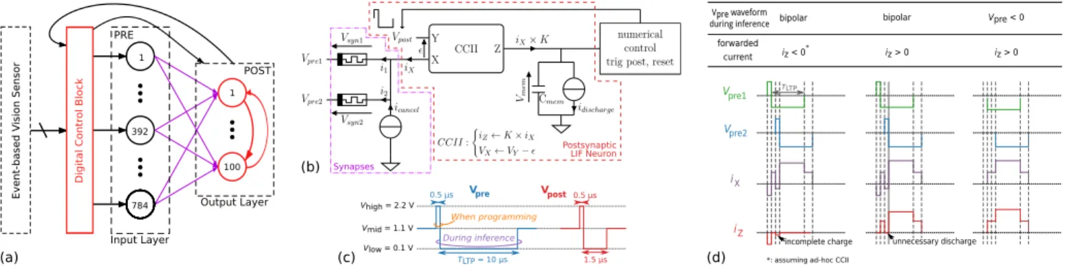
In this work, we study the architecture shown in Fig. 1(a) using a Python in-house simulator that allows high-level description of the behavior of each hardware building block.
Each output Leaky Integrate-and-Fire (LIF) neuron includes a second generation current conveyor [11], which allows to apply postsynaptic voltage pulses onto the memristive synapses (Fig. 1(b-c)). To save power the current conveyor only transmits current ifiX> 0. The output current iZ scales
iX by a factor K (constant in our simulations) in order to
Vpre1 Vpre2 iX iZ forwarded current iz < 0 iz > 0 iz > 0 Vpre waveform
during inference bipolar bipolar Vpre < 0
incomplete charge unnecessary discharge * Vmid = 1.1 V Vlow = 0.1 V Vhigh = 2.2 V V 0.5 µs 1.5 µs 0.5 µs TLTP = 10 µs pre V During inference When programming post 1 392 784 1 100 Event-based V ision Sensor Digital Contr ol Block PRE POST Input Layer Output Layer (a) (b) (c) (d) Postsynaptic LIF Neuron Synapses TLTP
*: assuming ad-hoc CCII
Fig. 1. Design overview. (a) System architecture: spiking neural network with Ninputs= 784 and Noutputs= 100 analog CMOS pre- and postsynaptic neurons
(numbered circles) fully connected through a single layer of memristive synapses with no selection device (purple arrows). An event-based vision sensor feeds the network while a digital control block supervises the analog neuron operation. (b) Circuit-level overview of one Leaky Integrate-and-Fire (LIF) postsynaptic neuron, which includes a second generation current conveyor (CCII) block that only forwards positive currents (i.e., iX> 0). In this sketch, two input pixels
are active and drive their respective memristor (devices on the left) while the rest of the memristive crossbar can be modeled as a current source (icancel). For
simplicity sake, we assume constant Vsyn= −1 V for active synapses. The control block on the right is actually part of the digital control block in (a). (c) The
pre- (left) and postsynaptic (right) voltage waveforms applied by the neurons. (d) Comparing input voltage waveform strategies for inference and illustrating the challenges of overlapping presynaptic waveforms, depending on Vprepolarity and the polarity of the current forwarded by the current conveyor.
Cmem ' 1 pF, while allowing to overcome the discharge
(∼ 100 V·s−1) due to the constant leakage currentidischarge=
100 pA over the timescale of the targeted patterns. An output event is generated when the membrane voltageVmemreaches a
threshold value (1 V in our simulations). Following a Winner-Take-All strategy, an output neuron that fires resets all the other output neurons. Besides, during training, a neuron that fired is reset until Nrefracother output neurons have fired (in
our simulationsNrefrac= 10), which prevents a single neuron
from overtaking all the activity.
To prevent the shadowing of input events due to overlapping presynaptic pulses (Fig. 1(d)), we split the presynaptic pulse waveform into two components (Fig. 1(c)) that are applied independently. Inference pulses of duration TLTP = 10 µs
are triggered by events received from the input visual sen-sor and can participate to synaptic long term potentiation. Shorter (0.5 µs) programming pulses can overlap with the low-amplitude part of a postsynaptic pulse for synaptic long term depression. From a circuit design viewpoint, the longer the time constants, the more chip area and energy is required.
If negative, the input voltage offsetε of the current conveyor (Fig. 1(b)) continuously charges the membrane capacitor, resulting in spurious output events. Thus, one must ensure a positive offset value, e.g., by adding a dedicated low-resolution digital-to-analog converter used to decrease the voltage offset at the network setup.
Many memristive technologies can have their conductance tuned by applying a voltage pulse beyond a threshold value [12]. Among them, ferroelectric memristors offer extremely low values of conductance [13]. For simplicity sake and simulation speed, here we consider that the memristive devices are programmed accordingly to
∆G =
+Apot× (Gmax− G0) for Vsyn≤ −1.2 V
−Adep× (G0− Gmin) for Vsyn≥ +1.2 V
0 otherwise
, (1) where G0, Gmin and Gmax are respectively the current, the
minimal and the maximal conductance values, Vsyn is the
voltage applied onto the memristor (Fig. 1(b)), andApot and
Adep are (dimensionless) learning rates. Eq. (1) is
reminis-cent of a multiplicative Spike-Timing Dependent Plasticity (STDP) learning rule implemented with rectangular program-ming pulses of constant amplitude and duration. The precise characteristics of the STDP should have only a limited impact on the insights provided by our study as several works have shown the high resilience of similar architectures to synaptic variability or STDP curves [14], [15]. Based on recent work on ferroelectric devices [16], we considerGminranging from1 nS
to10 nS and Gmax from0.1 µS to 1 µS. We use Apot =Adep
= 0.1, which allows single-epoch learning in our simulations. III. WHENONENEEDS ALONGERTERMINPUTMEMORY
In all our simulations, we replace the event-based visual sensor with the N-MNIST dataset, a conversion of the MNIST handwritten digit pictures to an event-based framework using a neuromorphic vision sensor [10]. Each one of the 60,000 (10,000) training (test) samples was generated through 3 consistent100 ms-saccades, resulting in 3 separate subclasses per digit class. Due to the limited amount of neurons in the hardware target, for each sample, we only use the data i) from the 28×28 central pixels ii) in the first saccade and iii) with ON polarity (i.e., increasing light events).
Fig. 2 illustrates a major issue of entirely implementing STDP through analog voltage overlapping. When an output neuron fires, because of the large mismatch between the analog hardware timescale (∼ TLTP= 10 µs) and the input event rate
(∼ 7000 events per second on average), only a handful of synapses are potentiated, and all the other ones are depressed. In our simulations, this leads to a∼ 0 % recognition rate.
To overcome this issue–unspecific to N-MNIST–we propose an STDP variation by introducing a digital control block (Fig. 1(a)) that allows tracking input activity and driving the programming events. To keep the CMOS overhead as low as possible, we use a 1-bit flag per presynaptic neuron that is set to ON when the neuron receives an input event. When a postsynaptic neuron fires, the synapses that are connected
0 1 2 3 4 5 6 7 8 9 Class 0 5 10 15 20 Max( Nev en ts in TLTP ) Overall Mean: 3.68TLTP= 0.01 ms
Fig. 2. For each digit class, statistics of the maximum amount of events (Nevents) that fall into a same long-term potentiation time window (TLTP)
over the first saccade of the 60,000 samples of the N-MNIST dataset. Gray large bars and black thin bars show the average value and the full range, respectively.
to it are then potentiated if their activity flag is ON and depressed otherwise. All presynaptic activity flags are then reset to OFF and we present the next digit sample. This form of STDP is thus entirely driven by postsynaptic events; each synapse connected to an output neuron that spikes is either potentiated or depressed, using separate pulses with constant duration and amplitude (translated into Eq. (1) first two lines in our simulations). This scheme is reminiscent of previous works in the literature [17], [18]. However, the time window that triggers long term potentiation is no more constant but depends on the last previous postsynaptic event. This makes the hardware implementation simpler: the timer needed for each presynaptic neuron is replaced with logic blocks.
Similarly to other works in the field, we focus on the subset of digits 5, 6 and 9 to reduce simulation time [19]. One epoch thus corresponds to 17,288 (2859) training (test) samples.
After training (for one epoch) and before testing, we dis-able output neurons that fired less than 10 times. For each remaining output neuron, if at least60 % of its last 10 events correspond to the same input class, we label it accordingly to the latter. Otherwise we disable the neuron. Empirically, this simple labeling strategy provides good agreement with labeling performed by a human, and the system achieves good selectivity (Fig. 3).
Without any device variability, the mean recognition rate is 92.4 % (Fig. 4(a)), close to the 93.68 % rate from the literature with a slightly different STDP and 400 output neurons [19].
1.0 0.0 0.2 0.4 0.6 0.8 Nor malized Condu ctan ce G /G max
(a) Output Neuron Label
Input
Sample Class
(b)
Fig. 3. Example of outcomes after one simulation run (Cmem = 1 pF,
ε = 0 mV, K = 1/125, initial weights uniformly distributed between Gmin = 10 nS and Gmax = 1 µS). (a) Some conductance maps used after
labeling. (b) Confusion matrix (on 2628 [218] correct [wrong] output events).
IV. IMPACT OFPOSTSYNAPTICNEURONVARIABILITY
In a hardware implementation, some dispersion will affect the characteristics of the postsynaptic neurons, like the current conveyor offset voltages or the membrane capacitor values.
The wider the range of offset voltages ε, the larger the currenticancel, which makes it harder for postsynaptic neurons
80 85 90 95 100 Recognition Rate (%) 0 1 2 3 4 0 (a) 0 1 2 3 4 0 20 40 60 80 100 Unlabeled Neurons (%) (b) Cmem= 1 pF Cmem∈ [0.8 pF, 1.2 pF]
Upper Bound for the Offset Voltage ε (mV)
Fig. 4. Impact of the current conveyor offset voltage (ε), without (black solid lines) and with uniformly distributed (gray dashed lines) dispersion of the postsynaptic neuron membrane capacitor values (Cmem). Random offset
voltages ε are uniformly drawn between 0 mV and the upper bound reported along the x-axis. Results without (with) membrane capacitor dispersion are averaged over 25 (125) one-epoch runs, combining 5 random sets of initial conductance values with 5 random sets of offset voltages (and with 5 random sets of membrane capacitors). The random sets are kept consistent between the simulations as much as possible. The other system parameters are the same as in Fig. 3. Symbols show the average values and the error bars show the full ranges. (a) The recognition rate, and (b) the fraction of output neurons (over Noutputs= 100 neurons) that are not used for classification after labeling.
to spike. This results in significantly less active and selective output neurons after training. Cadence®Virtuoso Monte Carlo
simulations of our current conveyor CMOS design suggest that the offset voltagesε may mostly lie between 1 mV and 2 mV. However, simulations of an even worse scenario (uniform distribution ofε from 0 mV to 4 mV) show that the recognition rate remains at87.3 % on average (solid black line in Fig. 4). Besides, adding a challenging uniform dispersion of the membrane capacitorCmem between±20 % around 1 pF
im-pacts only slightly more the performance (dashed gray line in Fig. 4). For example, the mean recognition rate drops to 86.9 % with the largest offset voltage dispersion.
The results in this section suggest that the mixed-signal architecture we propose should remain operational even with levels of postsynaptic circuit variability that are plausible in a hardware implementation, provided that the redundancy among output neurons is sufficient (Fig. 4(b)).
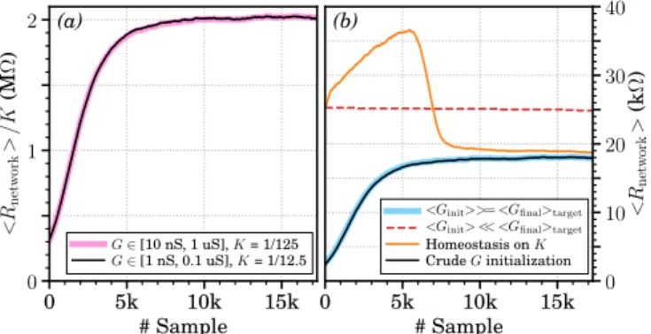
V. IMPACT OFINITIALWEIGHTDISTRIBUTION
The mean conductance values of the patterns learned by the system determine a (rough) suitable range for postsynaptic parameters like the current conveyor factor K. Hence it is to be expected that the final system performance depends on the initial conductance distribution. This section illustrates how < Rnetwork>, defined as the average resistance of the
Ninputsmemristors connected to each output neuron, evolves
in various situations and which challenges arise.
We typically scale the current conveyor factor K respec-tively to the average of the expected final conductance maps <Gfinal>target, in order to allow a reasonable triggering of
the output neurons after a successful learning. Then, starting from a smaller<Rnetwork> (i.e., <Ginit>≥<Gfinal>target)
allows output neurons to fire and to learn (thick blue line in Fig. 5(b), with a 92.3 % mean recognition rate after one
epoch). Besides in such a situation Fig. 5(a) shows that a system with 10 times more resistive synapses (solid black line) behaves similarly to a less resistive learning-capable system (thick pink line), provided thatK is made 10 times stronger; in both cases, the mean recognition rate is 92.3 %. If on the contrary <Rnetwork> is initially too large (i.e., <Ginit> <<
<Gfinal>target), the output neurons have difficulties to spike,
which results in unsuccessful one-epoch learning (dashed red line in Fig. 5(b)). 0 5k 10k 15k # Sample 0 1 2 < Rnet w ork > /K (M Ω ) (a) G∈ [10 nS, 1 uS], K = 1/125 G∈ [1 nS, 0.1 uS], K = 1/12.5 0 5k 10k 15k # Sample 0 10 20 30 40 < Rnet w ork > (k Ω ) (b)
<Ginit>>= <Gfinal>target <Ginit> << <Gfinal>target Homeostasis on K Crude G initialization
Fig. 5. Evolution of < Rnetwork> the average resistance value seen by
each output neuron. All results are averaged over five one-epoch simulation runs (ε = 0 mV and Cmem = 1 pF). (a) <Rnetwork> normalized by the
current conveyor factor K, when the synaptic crossbar is on average more resistive after the learning than initially. The thick pink line shows results with initial conductance values G uniformly distributed between 10 nS and 1 µS and K = 1/125 (average recognition rate [avgRR]: 92.3 %), while the thin black line corresponds to a case with ten times more resistive synapses and a factor K scaled accordingly (K = 1/12.5, avgRR: 92.3 %). (b) Illustration of challenges that arise when the synapses are initially more resistive on average than the patterns that would be learned after successful training. Conductance values can evolve between Gmin= 1 nS and Gmax= 1 µS. If not mentioned,
K=1/125. Solid thick blue line: a situation similar to (a), for reference purposes (avgRR: 92.3 %). All three other cases use initial conductance values that are uniformly distributed between Gminand Gmax/10. Dashed red line:
unchanged learning strategy (avgRR: 0 %). Solid orange line: applying some homeostasis onto K during the learning (starting from K = 1/12.5, avgRR: 92.4 %). Solid black line: half of the synapses are forcefully initialized to Gmaxbefore the learning (avgRR: 92.1 %).
A first approach to this challenge is to introduce an home-ostasis process for each postsynaptic neuron, e.g., on K. For example, starting with conductance values similar to the previous failed attempt but with K=1/12.5 and decreasing it by 0.001 (down to 1/125) each time the neuron spikes allows to reach a 92.4 % mean recognition rate (solid orange line in Fig. 5(b)). Another solution is to explicitly initialize the synapses to decrease <Rnetwork>. As an example, for each
output neuron, when initially arbitrarily programming half of the synapses to their maximum conductance value Gmax, the
system achieves92.1 % mean recognition rate (solid black line in Fig. 5(b)). Implementing the latter approach is likely to have a significantly smaller circuit-level overhead. Even the aforementioned crude memristor initialization allows to reach a good performance level; one could then simply leverage the programming blocks used for training to feed the digital control block with dedicated input events.
VI. CONCLUSION
To mitigate the short learning timescale of analog CMOS, we proposed adding a binary memory to each presynaptic
neuron. By simulation means, we illustrated the performance of our concept on the N-MNIST dataset and its resilience to neuron variability. We also studied how the initial synaptic weights impact the system operation, and how crude initial-ization or neuron homeostasis both mitigate this issue.
These results provide insights to build hardware spiking neural networks able to learn tasks with real-world timescales.
REFERENCES
[1] G. Indiveri and S. Liu, “Memory and information processing in neuro-morphic systems,” Proceedings of the IEEE, vol. 103, no. 8, 2015. [2] C. S. Thakur, J. L. Molin, G. Cauwenberghs, G. Indiveri, K. Kumar,
N. Qiao, J. Schemmel, R. Wang, E. Chicca, J. Olson Hasler, J.-s. Seo, S. Yu, Y. Cao, A. van Schaik, and R. Etienne-Cummings, “Large-scale neuromorphic spiking array processors: A quest to mimic the brain,” Frontiers in Neuroscience, vol. 12, 2018.
[3] Editorial, “Big data needs a hardware revolution,” Nature, vol. 554, no. 7691, 2018.
[4] Y. LeCun, Y. Bengio, and G. Hinton, “Deep learning,” Nature, vol. 521, no. 7553, 2015.
[5] S. Friedmann, J. Schemmel, A. Gr¨ubl, A. Hartel, M. Hock, and K. Meier, “Demonstrating hybrid learning in a flexible neuromorphic hardware system,” IEEE Transactions on Biomedical Circuits and Systems, vol. 11, no. 1, 2017.
[6] S. Moradi, N. Qiao, F. Stefanini, and G. Indiveri, “A scalable multicore architecture with heterogeneous memory structures for dynamic neuro-morphic asynchronous processors (DYNAPs),” IEEE Transactions on Biomedical Circuits and Systems, vol. 12, no. 1, 2018.
[7] M. Prezioso, M. Mahmoodi, F. M. Bayat, H. Nili, H. Kim, A. F. Vincent, and D. B. Strukov, “Spike-timing-dependent plasticity learning of coincidence detection with passively integrated memristive circuits,” Nature Communications, vol. 9, no. 1, 2018.
[8] Ultra-Low Power Event-Based Camera (ULPEC) H2020 project. [Online]. Available: http://ulpecproject.eu/
[9] C. Posch, T. Serrano-Gotarredona, B. Linares-Barranco, and T. Delbr¨uck, “Retinomorphic event-based vision sensors: Bioinspired cameras with spiking output,” Proceedings of the IEEE, vol. 102, no. 10, 2014.
[10] G. Orchard, A. Jayawant, G. K. Cohen, and N. Thakor, “Converting static image datasets to spiking neuromorphic datasets using saccades,” Frontiers in Neuroscience, vol. 9, 2015.
[11] G. Lecerf, J. Tomas, S. Boyn, S. Girod, A. Mangalore, J. Grollier, and S. Sa¨ıghi, “Silicon neuron dedicated to memristive spiking neural networks,” IEEE International Symposium on Circuits and Systems (ISCAS), 2014.
[12] D. Kuzum, S. Yu, and H.-S. P. Wong, “Synaptic electronics: materials, devices and applications,” Nanotechnology, vol. 24, no. 38, 2013. [13] A. Chanthbouala, V. Garcia, R. O. Cherifi, K. Bouzehouane, S. Fusil,
X. Moya, S. Xavier, H. Yamada, C. Deranlot, N. D. Mathur, M. Bibes, A. Barth´el´emy, and J. Grollier, “A ferroelectric memristor,” Nature Materials, vol. 11, no. 10, 2012.
[14] D. Querlioz, O. Bichler, P. Dollfus, and C. Gamrat, “Immunity to device variations in a spiking neural network with memristive nanodevices,” IEEE Transactions on Nanotechnology, vol. 12, no. 3, 2013.
[15] T. Serrano-Gotarredona, T. Masquelier, T. Prodromakis, G. Indiveri, and B. Linares-Barranco, “STDP and STDP variations with memristors for spiking neuromorphic learning systems,” Frontiers in Neuroscience, vol. 7, 2013.
[16] S. Boyn, J. Grollier, G. Lecerf, B. Xu, N. Locatelli, S. Fusil, S. Girod, C. Carr´et´ero, K. Garcia, S. Xavier, J. Tomas, L. Bellaiche, M. Bibes, A. Barth´el´emy, S. Sa¨ıghi, and V. Garcia, “Learning through ferroelectric domain dynamics in solid-state synapses,” Nature Communications, vol. 8, 2017.
[17] B. Nessler, M. Pfeiffer, L. Buesing, and W. Maass, “Bayesian compu-tation emerges in generic cortical microcircuits through spike-timing-dependent plasticity,” PLOS Computational Biology, vol. 9, no. 4, 2013. [18] D. Querlioz, O. Bichler, A. F. Vincent, and C. Gamrat, “Bioinspired programming of memory devices for implementing an inference engine,” Proceedings of the IEEE, vol. 103, no. 8, 2015.
[19] L. R. Iyer and A. Basu, “Unsupervised learning of event-based image recordings using spike-timing-dependent plasticity,” International Joint Conference on Neural Networks (IJCNN), 2017.