HAL Id: hal-01390969
https://hal.archives-ouvertes.fr/hal-01390969
Submitted on 2 Nov 2016HAL is a multi-disciplinary open access archive for the deposit and dissemination of sci-entific research documents, whether they are pub-lished or not. The documents may come from teaching and research institutions in France or abroad, or from public or private research centers.
L’archive ouverte pluridisciplinaire HAL, est destinée au dépôt et à la diffusion de documents scientifiques de niveau recherche, publiés ou non, émanant des établissements d’enseignement et de recherche français ou étrangers, des laboratoires publics ou privés.
Piezo-generator integrating a vertical array of GaN
nanowires
N Jamond, P Chrétien, F Houzé, Lu Lu, L Largeau, O Maugain, L Travers,
J-C Harmand, F Glas, E Lefeuvre, et al.
To cite this version:
N Jamond, P Chrétien, F Houzé, Lu Lu, L Largeau, et al.. Piezo-generator integrating a vertical array of GaN nanowires. Nanotechnology, Institute of Physics, 2016, 27, pp.325403. �10.1088/0957-4484/27/32/325403�. �hal-01390969�
Piezo-Generator Integrating Vertical Array of GaN Nanowires
N. Jamond1, P. Chrétien2, F. Houzé2, L. Lu3, L. Largeau1, O. Maugain1, L. Travers1,
J. C. Harmand1, F. Glas1, E. Lefeuvre3,M. Tchernycheva3, N. Gogneau1,*
1 Laboratoire de Photonique et de Nanostructures, CNRS, Université Paris-Saclay, Route de Nozay, F-91460 Marcoussis, France
2 Laboratoire de Génie Électrique et Électronique de Paris (GeePs), UMR 8507 CNRS-Centrale Supélec, Université Paris-Sud et UPMC, 11 rue Joliot-Curie, Plateau de Moulon, 91192 Gif-sur-Yvette, France
3Institut d'Electronique Fondamentale, CNRS UMR 8622, Université Paris-Saclay, 91405 Orsay, France
Keywords: GaN nanowires, Piezoelectricity, Piezo-generator, Energy harvesting
Abstract
We demonstrate the first piezo-generator integrating a vertical array of GaN NWs. We perform a systematic multi-scale analysis, going from single wire properties to macroscopic device fabrication and characterization, which allows to establish for GaN NWs the relationship between the material properties and the piezo-generation and to propose an efficient piezo-generator design. The piezo-conversion of individual MBE-grown p-doped GaN NWs in a dense array is assessed by atomic force microscopy equipped with Resiscope module yielding an average output voltage of 228 ± 120 mV and a maximum value of 350 mV generated per NW. In the case of p-doped GaN NWs, the piezo-generation is achieved when a positive piezo-potential is created inside the nanostructures, i.e. when the NWs are submitted to a compressive deformation. The understanding of the piezo-generation mechanism in our GaN NWs gained from AFM analyses is applied to design a piezo-generator operated under compressive strain. The device consists of NW arrays of several square millimeters in size embedded into spin-on glass with a Schottky contact for rectification and collection of piezo-generated carriers. The generator delivers a maximum power density of ∼12.7 mW/cm3. This value settles the new state of the art for piezo-generators based on GaN NWs and more generally on Nitride NWs, and offers promising prospects for the use of GaN NWs for high-efficiency ultra-compact energy harvesters.
Introduction
A new worldwide challenge consists in the development of autonomous micro-devices, such as sensors for environment or nomad electronics. Today, most of these micro-devices are still powered by batteries, which present the issues of a limited lifetime and a difficulty of miniaturization. Thanks to recent technological progress leading to the reduction of the power consumption of the micro-devices down to the mW or even to the µW level, the energy harvesting systems appear as a promising power source. Among the alternative sustainable energy resources, the mechanical deformations (e.g. vibrations, friction, body movements or sound) present the advantages of being ubiquitous, available at all time and more accessible than solar and thermal energies. The generators harvesting these ambient energies, found in the vicinity of the device, are based on piezoelectric materials [1-2].
One-dimensional nanostructures, such as nanowires (NWs) presenting piezoelectric properties, have recently emerged as excellent candidates to fabricate novel ultra-compact and efficient piezoelectric generators. Thanks to their superior mechanical properties [3-4] (larger elastic deformation, higher flexibility and resistance), higher sensitivity to applied force [4-5] and higher piezoelectric response [6-8] with respect to the bulk material, the NWs present key advantages to fundamentally improve the generator performance.
Since the first demonstration of electrical energy generated by bending single ZnO NWs [9], the mechanical to electrical energy conversion has been demonstrated for other piezoelectric 1D-nanostructures, such as CdS [10], CdSe [11], PZT [12], BaTiO3 [13],
KNBO3 [14] etc. These studies of nanogeneration of individual semiconductor NWs have
naturally lead to the development of micro- and millimetric NW-based piezo-generators. To avoid confusion existing in the literature, in this paper we define a “nanogenerator” as a single NW having the ability to convert a mechanical deformation into electrical energy; while we call “NW-based piezo-generator” a macroscopic device integrating an array of 1D
nanostructures (i.e. an array of nanogenerators) and generating piezoelectric energy in response to its deformation.
Piezo-generators integrating 1D-nanostructures have been intensively studied with the development of different designs, such as generators based on vertically aligned NWs [15-18] or horizontal NWs [17, 19] array, either on flexible [15, 19] or hard [16-18] substrates. Generators based on ZnO NWs [15-19], PVDF nano-materials [20], PZT nanofibers [21] and GaN NWs [22-23] have been developed with power density in the µW-mW/cm3 range. From
ZnO NWs based piezo-generator prototypes, self-powered nano-systems without external battery have been demonstrated including pH and UV [24], chemical [25] and biological sensors [26], commercial light-emitting diodes (LED) [27], liquid-crystal-display (LCD) screen [28] or wireless radio frequency data transmitter [29].
Compared to ZnO, the III-nitride NWs have been much less studied for piezo-generation in spite of their high piezoelectric coefficients [30]. The concept of nanogenerator for III-nitride nanostructures has been demonstrated for the first time in 2007 by bending GaN nanorods [31]. More recently, their strong piezo-generation responses have been reported, with output voltages ranging from several millivolts to 440 mV for GaN [22] and to 1 V [33] for InN single NWs. These outputs largely exceed those generated by other piezoelectric nanostructures and especially by single ZnO NWs (e.g. 45 mV [34] and 80 mV [35] for respectively n-doped and p-doped ZnO, which are the most widespread nanomaterials integrated into NW-based piezo-generators). To date, several groups have presented AFM characterizations of single piezoelectric properties of nitride NWs [32-33, 36-38]. On the basis of these nanogenerator demonstrations, obtained by atomic force microscopy, maximum power densities reaching few hundred of mW/cm2 have been estimated [32, 36], which
demonstrates the high promise of the III-Nitride nanostructures for efficient piezo-generators. However, despite these promising results, only few NW-based piezo-generators integrating
nitride NWs have been reported in the literature, delivering power density not exceeding few hundred of µW/cm3 (calculated from the published data) [22-23].
In this paper, we demonstrate the first piezo-generator integrating dense array of vertical GaN NWs as the converting medium. The array of self-assembled NWs was grown by PA-MBE on Si(111) substrate. The NW piezo-generation was first characterized at the nanoscale by using AFM microscope equipped with a modified Resiscope module yielding an average output voltage of 228 ± 120 mV generated per NW (the maximum value being 350 mV). We show that in the studied case of N-polar p-doped GaN NWs, the piezo-generation occurs when the nanostructures are submitted to a compressive strain, i.e. when a positive piezo-potential is created inside the NWs. The fine understanding of the relationship between the material properties and the piezoelectric generation gained from AFM analyses has been applied to design a piezo-generator operating under compressive strain. The fabricated device consists of NW arrays of several square millimeters in size embedded into spin-on glass with a Schottky contact for rectification and collection of piezo-generated carriers. The maximum power density produced by this prototype is 12.7 mW/cm3, which largely exceeds the one
delivered by the previously reported piezo-generators based on Nitrides NWs [22-23]. The delivered power is reproducible (i.e. it is obtained repeatedly for each loading cycle and for various frequencies). This result establishes the new state of the art for GaN NW-based piezo-generator performance.
Methods
Self-assembled GaN NWs were grown by plasma-assisted molecular beam epitaxy (PA-MBE) on n-type doped Si(111) substrate. The NW growth was performed at 760 °C under N-rich conditions with an N/Ga ratio of about 1.36, the active nitrogen being supplied by a radio-frequency plasma cell. During the growth, the Mg cell was kept at 400 °C in order to
induce a p-type residual doping of GaN NWs. Prior to the growth of GaN NWs, a 2.5 nm-thick AlN buffer layer was deposited, allowing for a better control of the NW nucleation, density and orientation [39-41]. This AlN interlayer could be considered as a potential barrier preventing the circulation of piezoelectric charges, however as discussed below this is not the case. To form this thin AlN interlayer, the deoxidized Si(111) substrate is firstly exposed at 600°C to an Al flux and secondly only to a nitrogen flux (by switching the Al/N shutters), forming then the AlN layer [42]. The pre-deposition of the Al adatoms on the Silicon surface induces the formation of the Al-Si eutectic of composition x = 0.126 [43]. During the nitridation phase, the Si adatoms are incorporated into the AlN layer, producing an efficient n-doping and thus yielding a conductive behavior (which is supported by the output voltages measurement presented below). The growth of this AlN interlayer following this procedure is beneficial for piezo-conversion since it prevents the formation of the insulating SiN layer between the GaN NWs and the Si(111) substrate, which annihilates the piezoelectric generation.
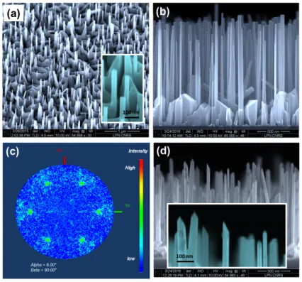
Figure 1a shows the typical p-doped GaN NW morphology. The GaN NWs grown under these conditions present a hexagonal cross section bounded by {10-10} planes [44] and they are vertically aligned as demonstrated by the XRD pole figure (Fig. 1c). Pole figures, which provide the in-plane orientation of NWs, were recorded by using the Bragg reflection of GaN (10-11) planes which are inclined by 62° from the [0001] direction (instrumental resolution of the measurements was 0.5°). The high diffracted intensity at the sample inclination for α = 62° established that the growth direction of the wire (c-axis) is normal to the Si(111) substrate surface.
The GaN NWs are characterized by a height of 1 µm ± 120 nm, a diameter of 45 nm ± 20 nm and a density of the order of 3x10⁹ NWs/cm². The NW heights have been determined from
AFM measurements in tapping mode, while the diameter and the density have been extracted from SEM images in top-view.
It is important to remind, that the GaN NWs are characterized by a wurtzite crystal structure, which does not have inversion symmetry. Within wurtzite material, the (0001) and (000–1) surfaces, namely metal polarity and N polarity respectively, are not equivalent and present different properties, such as different surface morphologies, optical and kinetic properties [45-47]. The polarity of the material is of crucial importance for the piezo-generation properties, since it sets the orientation of the internal polarization. The latter consists of the sum of the spontaneous polarization (PSP) and of the piezoelectric polarization (PPZ), which results from
the relative displacement of the Ga cations with respect to the N anions along the deformation direction when a stress is applied to the NW. In order to determine the polarity of our p-doped GaN NWs, we have dipped the nanostructures into a KOH aqueous solution. This etching treatment is known to reveal the polarity of GaN surfaces. In fact, hydroxide ions etch the Ga atoms but are repelled by the electronegativity of the nitrogen dangling bond. In consequence, the morphology of Ga-polar surfaces is preserved [48], while the N-polar surfaces are modified with the appearance of tilted {10-1-1} planes [49]. Figure 1d presents SEM image of the morphology of vertical array of p-doped GaN NWs etched for 5 min in 0.5 M KOH solution at 40°C. The observed pyramidal features on the top facet of all the NWs are the typical signature of etched N-polar surfaces. We can thus conclude that in our case, the GaN NWs are characterized by a Nitrogen polarity as previously evidenced by CBED observations and KOH etching [42]. In these conditions, PSP, which is oriented from N to Ga atoms, is
parallel to the growth direction and PPZ is anti-parallel (parallel) to the Z axis under
compression (stretching) along the c-axis. Consequently, the resulting piezoelectric potential created inside the nanostructures is positive under compressive strain and negative under tensile strain [50].
Figure 1: Tilted (a) and cross-section (b) SEM images of Mg-doped GaN NWs
grown by PA-MBE on Si(111) substrate. (c) X-ray pole figures for GaN NWs recorded by using the Bragg reflection of GaN (10-11) planes. The high diffracted intensity at the sample inclination for 62° from the [0001] direction demonstrates that the growth direction of the wire is normal to the substrate surface. (d) SEM image of Mg-doped GaN NWs after dipping into KOH etchant. The pyramidal top facet of the NWs is a signature of N-polar surfaces.
The piezoelectric properties of GaN NWs have been characterized with an atomic force microscope (AFM) equipped with a modified Resiscope module [51]. This technique combines the advantages of the nanometer scale resolution of the AFM and the real-time electrical measurements of the Resiscope. During scanning over the array of vertical NWs, the conductive AFM tip induces a local bending of the nanostructures. In response to this deflection and due to the piezoelectric effect, the NWs generate a voltage which is detected through the conductive AFM tip. We note that the used AM tip was coated with PtIr since this materials brings the best harvesting efficiency among the others available coatings [52]. Throughout the measurements, both the topographic and the electrical signals were recorded continuously and simultaneously. In this measurement method, the external electrical circuit
is connected via an ohmic contact formed between the NWs [53] and the substrate, and a Schottky contact formed between the NW top and the AFM tip [50]. No external voltage is applied and the voltage waveform generated by the NW is observed across a load resistance
RL of 1 GΩ.
The piezo-generator device integrating the vertical array of GaN NWs has been tested under bending. The bending was applied by a cylinder localized below the center of the device inducing a vertical movement, while the extremities of the device were clamped. The bending has been measured with a Keyence laser sensor, which allows a real-time monitoring of the displacement of the piezo-generator center, while the force applied by the cylinder on the sample has been computed by simulation from the displacement measurement. Finally, the electrical measurements have been performed with a Keysight MSOX3034T Oscilloscope, with an internal impedance of 1 MΩ, by connecting respectively the ground and the input of the oscilloscope to the ohmic and Schottky contacts of the piezo-generator.
Results and Discussion
Piezo-generator performance depends primarily on the piezoelectric properties of the active material, which in the present case consists of a layer of vertical GaN NWs. In order to take full advantage of the piezo-conversion capacity of the NWs and to choose the correct design, it is of crucial importance to assess the properties of these nanostructures. To this end, the piezoelectric properties of the N-polar GaN NWs have been characterized with the AFM-Resiscope [51]. Figure 2 presents the topographic image and the corresponding 3D image of output voltage peaks from an array of GaN NWs recorded for a constant normal AFM tip force of 149 nN. We note here that this constant normal force is much higher than the one used for characterizing free standing ZnO NWs (5 nN) [9]. In fact, our GaN NWs are characterized by a high flexibility. In order to avoid folding them completely down to the
substrate which would lead to a leakage of piezoelectric charges and thus to an inhibition of the piezo-conversion, we have partly mechanically consolidated them [32]. Consequently, a higher deflection force is needed to bend the partly consolidated NWs to a similar degree of deformation as the free-standing nanostructures.Each peak corresponds to the piezo-response of an individual NW. We note that since the GaN NWs are probed with the same constant normal AFM tip force during a scan, the output signal distribution reflects the dimensional dispersion of the NWs (resulting from the self-assembled growth mode used to synthesize them). Each output peak exhibits a positive voltage that indicates a p-type conductivity of the nanostructures [54] (in agreement with the growth conditions). From the statistical analysis of the 3D output voltage mapping, we measure that the GaN NWs generate an average output voltage of 228 ± 120 mV and a maximum of 350 mV per NW. These values largely exceed the maximum voltage generated by single ZnO NWs (45 mV [34] and 80 mV [35] respectively for n-doped and p-doped ZnO NWs), and demonstrates the promise of GaN nanostructures to develop high-efficient piezo-generators.
Figure 2: (a) Topographic image and (b) corresponding 3D output voltages collected by AFM-Resiscope on p-type GaN NWs for a constant normal force of 149 nN. The average and maximum output voltages generated by the GaN NWs are respectively equal to 228 ± 120 mV and 350 mV.
The development of high-efficient NW-based piezo-generators requires a fine understanding of the piezoelectric conversion mechanisms in individual NWs. With the nanometer scale resolved AFM technique, which allows the simultaneous recording of topographic and electrical signals, it is possible to directly correlate the morphology of a given bended NW with its generated voltage peak. This correlation has been established by Su et al. [31] and Gogneau et al. [50], then highlighting that the piezo-generation of N-polar n-doped GaN nanostructures is always observed when the AFM tips gets in contact with the stretched side of the bended GaN nanostructures, i.e. when a negative piezo-potential is created inside the nanostructures. By considering this mechanism, the piezo-generation of N-polar GaN NWs but with a p-type doping should be detected on the compressive side of the NWs. In order to verify this point, we have superimposed topography and voltage profiles together with a schematic representation of the tip position on the NW (Fig. 3a). Hence, we observe that the output signal is generated only when the AFM tip is in contact with the compressed side of the NW. This observation indicates that in the case of N-polar p-type GaN NWs, the Schottky diode formed at the NW top/AFM tip interface is positively biased when the nanostructure is characterized by a compressive strain and thus by a positive piezo-potential [50, 54]. Hence, only under compression, the piezoelectric NW (nitrogen-polar and p-doped) acts as a generator. Now we transpose this piezo-conversion mechanism to a NW-based piezo-generator, in which the array of vertical NWs is submitted to an axial compression. The underlying piezo-generation mechanism is schematized in figure 3b. When the axial compression is applied (straining state), the Schottky diode formed at the NW/electrode interface is forward biased. The electrons from the external circuit can thus
flow into the semiconductor in order to compensate the positive piezo-potential. By contrast, when the strain is released, the Schottky contact is reverse biased, preventing the electrons to flow back through the top electrode and force them to the external circuit via the ohmic contact, insuring electrical neutrality of the unstrained semiconductor crystals.
Figure 3: (a) Corresponding topographic and electric profiles of GaN NWs
characterized by AFM-Resiscope. The output signal (in red) is detected when the tip is in contact with the compressed side of the NW (represented in blue). The diode is positively biased when the nanostructure is characterized by a compressive strain inducing a positive piezo-potential inside the NW. We note here that on topographic profile, the NW diameter is oversized in comparison with the real one due to the tip/surface convolution. (b) Schematic illustration of the electrical generation mechanism for an array of vertical N-polar p-doped GaN NWs involved in a piezo-generator device, in the case of strained state (axial compression) and strain releasing.
The performance of NW-based piezo-generators is determined by the ability of the active layer (array of NWs) to efficiently convert a mechanical deformation into an electrical energy, by the efficiency of the energy harvesting, and more generally by the design of the device. Concerning the first point, in this paper we use high density N-polar p-type GaN NWs, which are characterized by a high piezoelectric response (with outputs reaching 350 mV per NW in
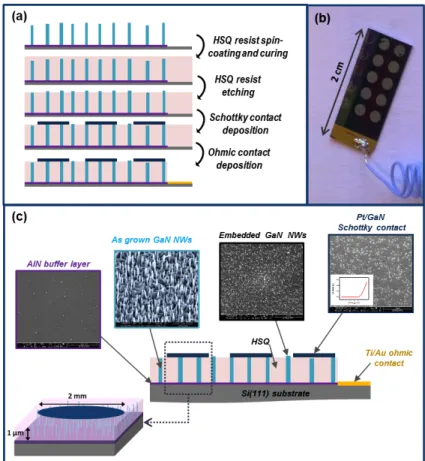
figure 2). Regarding the second point, in a recent study we have shown that the use of Platinum-based Schottky contact is optimal to harvest the energy piezo-generated by GaN NWs [52]. Therefore, in the present paper we have used Pt-based contact, which we think contributes to increase the output power of the demonstrated device. Regarding the last point, we have established the relationship between the material properties and the piezo-generation mechanism. Namely in the case of our N-polar p-type GaN NWs, the piezo-generated energy is detected when the nanostructures are submitted to a compression strain state (figure 3). Hence, the device architecture, integrating N-polar p-type GaN array and relying on a compressive strain, was chosen. Figure 4a describes the fabrication process of a NW-based piezo-generator integrating a dense array of N-polar p-doped GaN NWs. First, the as grown GaN NW array was embedded into a hydrogen silsesquioxane resist (HSQ) [55] by spin-coating and then thermally cured at 400 °C for 1h under nitrogen at atmospheric pressure. The choice of the HSQ is motivated by the fact that the silica matrix has a strong mechanical adherence to the NWs. It thus insures the transmission of the applied deformation to the nanostructures in a homogeneous way, while conferring a mechanical stability to the ensemble. Second, reactive ion etching (RIE) with SF6 and CHF3 reactive gases was used to
etch-back the HSQ and to uncover the top portion of the NWs (∼100 nm). Then, the Schottky contact, consisting of 5 nm of Cr and 200 nm of Pt, was deposited through a shadow-mask on the top of the NWs. The Pt based-Schottky contact was chosen since it provides a diode low reverse leakage while the barrier height remains moderate, which allows to efficiently harvest the generated piezo-energy, as previously demonstrated [52]. Finally, the ohmic contact, consisting of a bilayer Ti/Au (10 nm/150 nm), has been deposited directly on the Si(111) substrate. Figure 4a illustrates the above-describe piezo-generator fabrication steps. The effective size of the devices and SEM images illustrating the different fabrication steps are shown in figures 4b and 4c.
Figure 4: (a) Schematization of the piezo-generator fabrication process. (b)
Optical image of the processed piezo-generator. (c) Schematic of the device and SEM images illustrating each step of the fabrication process.
The piezo-generator device integrating the vertical array of GaN NWs has been tested by compressive solicitation. In order to homogeneously strain the active layer, the generator is bended by inducing a vertical movement via a cylinder with a controlled displacement. We would like to stress that the solicitation force used to characterize the NW-based piezogenerator (maximum 1.5 N) does not induce any damage in the Si(111) substrate. No cracks or cleavage marks have been observed by optical microscopy and SEM after solicitation tests. We also note that no degradation of electrical properties has been evidenced after about 100 bending cycles. The figure 5a schematizes the solicitation mode. Due to the difference of thickness between the substrate (350 µm) and the active layer (∼ 1 µm) and due to the strong mechanical adherence of the HSQ matrix to the NWs, the lateral bending of the device induces stretching of the matrix and, as a consequence of the volume conservation, a thinning of the active layer. This matrix
deformation is transmitted to the embedded GaN NWs leading to their homogeneous compression, as illustrated on figure 5b. We note that under these mechanical solicitation conditions, one cannot exclude that in addition to the axial compression induced by the mechanical thinning of the HSQ matrix a small lateral bending of the nanostructures can be induced. The lateral NW curvature leads to a piezo-potential distribution evolving between a negative value on the stretched side of the NW and a positive value on the compressed side of the NW [9, 50]. However, the Schottky contact of the piezo-generator covering the entire NW top, a conducting channel would be created between the both NW sides, leading to the neutralization of the piezoelectric charges and thus no output voltage could be measured. Therefore, we can assume that the piezo-potential induced by small lateral NW bending does not contribute to the generation in the present device architecture [9].
Figure 5c presents the output voltage generated by the GaN NW-based piezo-generator synchronized with the magnitude of the force applied to bend the device. The piezo-generator has sustained a large amount of bending cycles (more than 103), with a frequency ranging
from 1 to 6 Hz and a maximum applied force of about 1.5 N. The piezo-generated voltage is clearly correlated with the applied deformation.
For low frequency solicitation, a signal drop is observed when the applied force reaches its maximum. This behavior may be due to the transitory nature of the generation and to the low frequency of the solicitation. The current crossing the device (translated into the measured output voltage) is proportional to d(ɛ)/dt, where ɛ is the deformation of the device. When the deformation reachs its maximum, d(ɛ)/dt becomes zero and thus the measured output should decrease due to discharging of the generator through the load circuit. This hypothesis is supported by the fact that at 3 Hz the signal drop is more pronounced than at 6 Hz. Further investigations and modeling are currently in progress in order to explain the observed signal time variation.
Figure 5: (a) Schematic of the setup used to characterize the GaN NW-based
piezo-generator. The lateral bending of the generator induces a thinning and thus a compression of the active layer as illustrated in (b). (c) Output voltages generated by the piezo-generator as a function of its deformation for a bending cycle rate of 3 Hz (top) and 6 Hz (bottom). (d) Band diagram of the interface between the top of GaN NWs and the Pt electrode. The red dashed lines illustrate the modulation of the Schottky barrier height due to the induced piezo-potential.
The observed square-like signal in response to a sinusoidal force can be understood by the piezoelectric mechanisms into play. At the beginning of the bending cycle, for small deformations, the compression of the active layer is not sufficient to create the internal piezoelectric potential necessary for carriers to cross the Schottky barrier [37]. For higher deformation, the piezo-potential becomes sufficient to open the Schottky barrier and thus piezoelectric signal can be measured. However, the generation does not increase proportionally to the NW deformation as demonstrated by X. Xu et al. [37], but grows faster than the deformation (square output signal versus sinusoidal signal), until reaching the saturation. This behavior is directly correlated to the increase of the piezo-potential amplitude
inside the nanostructure with the deformation state and to its influence on the Schottky diode. In fact, the positive piezo-potential at the semiconductor side effectively reduces the Schottky barrier height, as illustrated by the energy band diagram in figure 5d [56-57]. This phenomenon gives rise to an increase of voltage collection at the interface and thus to a higher piezoelectric energy harvested. To explain the observed saturation of the output voltage, a saturation of the internal electric field inside the NWs resulting from the saturated rotation of electric dipoles [58] or a possible limitation of the harvested energies though the Schottky contact as observed previously [52] can be considered. Further investigations are in progress to clarify this point.
Finally, whatever the solicitation conditions (number of cycles and frequency in the 1 to 6 Hz range), the GaN NW-based piezo-generator always exhibits a saturated maximal output voltage of about 200 mV. By considering the square-like signal of the output, we determine the average output power generated by our device in one stimulation event by using the following relation: ΡAverage=V 2i2 RL, while the maximum power can be calculated following
the equation: ΡMax =Vi2 RL, where
i
V is the output voltage generated by the active layer and
L
R is the load resistance used in the measurement (RL = M1 Ω). Knowing that the solicited piezoelectric active region has a cylinder shape with a diameter of 0.2 cm and a height of 1 µm (Fig. 4c), the effective volume,VPZ, is of the order of 3.14x10
-6 cm3. The piezoelectric
output being equal to 200 mV by this active volume, we estimate an average output power density of 6.35 mW/cm3, and a maximum output power density of about 12.7 mW/cm3. These
two values exceed largely the power density generated by the previously reported generators based on nitride NWs [22-23] and establish the new state of the art for piezo-generators based on III-N NWs.
These very promising results enable to envision various practical applications of nitride NW-based energy harvesting devices. In particular, they would be very interesting in medical applications such active implants, in which they could profitably replace batteries by bringing significant lifetime extension of the implants [59]. The very small power needs of active implants, about 1 µW in the case of the last generation leadless pacemakers, would be attainable using only 0.157 mm3 nitride NW active material. As shown here, nitride NWs are capable to generate power from very low mechanical frequencies, making this active material perfectly compatible with the typical human mechanical frequency spectrum [60]. Moreover, the generated power exhibits very interesting stability versus the frequency variations. According to state of the art of nanopower energy harvesting electronic interface circuits, piezoelectric voltages as low as 200 mV can be stepped-up to applications requirements, typically in the range of 1.2 V to 5 V, with more than 80% energy efficiency [61].
4. Conclusion
In conclusion, we have demonstrated the fabrication of the first piezo-generator integrating vertical array of GaN NWs. The piezoelectric properties of the GaN NWs array have been investigated by AFM Resiscope, yielding an average output voltage of 228 ± 120 mV and a maximum voltage of 350 mV per NW. The comparison between the topography and output voltage profiles allowed us to highlight that the piezoelectric conversion in the N-polar p-doped GaN NWs is achieved when a compressive strain and thus a positive piezo-potential are created inside the nanostructures. Based on the single NW characterizations, we have designed a NW-based piezo-generator integrating vertical array of GaN NWs operating under compressive strain. This prototype delivers a maximum power density of 12.7 mW/cm3
measured power density defines the new state of the art and offers promising prospects for the development of high-efficiency and ultra-compact piezo-generators based on GaN NWs.
Acknowledgments
This work was supported by the by EU Horizon 2020 ERC project “NanoHarvest” (Grant 639052), the French National Research Agency though the GANEX program (ANR-11-LABX-0014) and the Region Ile-de-France in the framework of DIM Nano-K and ESSEN project. The authors are also grateful to Hezhi Zhang for fruitful discussions.
References
[1] Wang Z L, Wu W 2012 Angewandte Chemie International Edition 51 11700. [2] Hudak N S, Amatucci G G 2008 J. Appl. Phys. 103101301.
[3] Wen B, Sader J E, Boland J J 2008 Phys. Rev. Lett. 101 175502. [4] Wang X 2012 Nano Energy 1 13.
[5] Zhou Y S, Hinchet R, Yang Y, Ardila G, Sangmuang R, Zhang F, Zhang Y, Han W, Pradel K, Montès L, Mouis M, Wang Z L 2013 Adv. Mater. 25 883.
[6] Minary-Jolandan M, Bernal R A, Kuljanishvili I, Parpoil V, Espinosa H D 2012 Nano
Lett. 12 970.
[7] Zhao M H, Wang Z Lmao , S X 2004 Nano Lett. 4 587. [8] Agrawal R, Espinosa H D 2011 Nano Lett. 11 786. [9] Wang Z L 2006 Science 312 242.
[10] Lin Y F, Song J, Ding Y, Lu S Y, Wang Z L 2008 Appl. Phys. Lett. 92 022105.
[11] Zhou Y S, Han W, Rai S C, Zhang Y, Ding Y, Pan C, Zhang F, Zhou W, Wang Z L 2012
ACS Nano 6 6478.
[12] Chen C Y, Liu T H, Zhou Y, Zhang Y, Chueh Y L, Chu Y H, He Jr H, Wang Z L 2012
Nano Energy 1 424.
[13] Wang Z, Hu J, Suryavanshi A P, Yum K, Yu M F 2010 Nano Lett. 10 2966. [14] Kang P G, Lee T K, Ahn C W, Kim I W, Lee H H, Choi S B, Jung J H 2015 Nano
Energy 17 261.
[15] Opoku C, Dahiya A S, Oshman C, Cayrel F, Poulin-Vittrant G, Alquier D, Camara N 2015 Physics Procedia 70 858.
[16] Cha S N, Seo J S, Kim S M, Kim H J, Park Y J, Kim S, Kim J W 2010 Adv. Mater. 22 4726.
[18] Zhu G, Wang A C, Liu Y, Zhou Y, Wang Z L 2012 Nano Lett. 12 3086. [19] Yang R, Qin Y, Dai L, Wang Z L 2009 Nat. Nanotechnol 4 34.
[20] Chang C, Tran V H, Wang J, Fuh Y K, Lin L 2010 Nano Lett. 10 726. [21] Chen X, Xu S, Yao N, Shi Y 2010 Nano Lett. 10 2133.
[22] Lin L, Lai C H, Hu Y, Zhang Y, Wang X, Xu C, Snyder R L, Chen L J, Wang Z L 2010
Nanotechnology 22 475401.
[23] Liu G, Zhao S, Henderson R D E, Leonenko Z, Abdel-Raman A, Mi Z, Ban D
Nanoscale, DOI: 10.1039/C5NR06841J
[24] Xu S, Qin Y, Xu C, Wei Y, Yang R, Wang Z L 2010 Nat. Nanotechnology 5 366 [25] Li Z, Zhu G, Yang R, Wang A C, Wang Z L, 2010 Adv. Mater. 22 2534.
[26] Lee M, Bae J, Lee J, Lee C S, Hong S, Wang Z L 2011 Energy Environ. Sci. 4 3359. [27] Zhu G, Yang R, Wang S, Wang Z L 2010 Nano Lett. 10 3151.
[28] Hu Y, Xu C, Zhang Y, Lin L, Snyder R L, Wang Z L 2011 Adv. Mater. 23 4068. [29] Hu Y, Zhang Y, Xu C, Lin L, Snyder R L, Wang Z L 2011 Nano Lett. 11 2572. [30] Bernardini F, Fiorentini V, Vanderbilt D 1997 Phys. Rev. B 56 R10024(R). [31] Su W S, Chen Y F, Hsiao C L, Tu L W 2007 Appl. Phys. Lett. 90 063110.
[32] Gogneau N, Chrétien P, Galopin E, Guilet S, Travers L, Harmand J C, Houzé F 2014
Phys. Status Solidi RRL 8 414.
[33] Huang C T, Song J, Tsai C H, Lee W F, Lien D H, Gao Z, Hao Y, Chen L J, Wang Z L 2010 Adv. Mater. 22 4008.
[34] Gao P X, Song J, Liu J L, Wang Z L 2007 Adv. Mater. 19, 67.
[35] Lu M P, Song J, Lu M Y, Chen M T, Gao Y, Chen L J, Wang Z L 2009 Nano Lett. 9 1223.
[36] Chen C Y, Zhu G, Hu Y, Yu J, Song J W, Cheng K Y, Peng L H, Chou L J, Wang Z L 2012 ACS Nano 6 5687.
[37] Xu X, Potié A, Songmuang R, Lee J W, Bercu B, Baron T, Salem B L, Montès L 2011
Nanotechnology 22 105704.
[38] Wang X, Song J, Zhang F, He C, Hu Z, Wang Z L 2010 Adv. Mater. 22 2155.
[39] Brubaker M D, Levin I, Davydov A V, Rourke D M, Sanford N A, Bright V M, Bertness K A 2011 J. Appl. Phys. 110 053506.
[40] Songmuang R, Landré O, Daudin B 2007 Appl. Phys. Lett. 91 251902.
[41] Bertness K A, Roshko A, Mansfield L M, Harvey T E, Sanford N A 2007 J. Cryst.
Growth 300 94.
[42] Largeau L, Galopin E, Gogneau N, Travers L, Glas F, Harmand J C 2012 Cryst. Growth
Des. 12 2724.
[43] Massalski, T. B. 1986 Binary Alloy Phase Diagrams, Eds.; American Society for Metals:
Metals Park, OH 1 164.
[44] Largeau L, Dheeraj D L, Tchernycheva M, Cirlin G E, Harmand J C 2008 Nanotechnogy
19 155704.
[45] Randall M M, Northrup J E, Neugebauer J 2002 MRS Internet J. Nitride Semicond. Res.
7 3.
[46] Huang D, Reshchikov M A, Visconti P, Yun F, Baski A A, King T, Morkoc H, Jasinski J, Liliental-Wever Z, Litton C W 2002 J. Vac. Sci. Technol. B 20 2256.
[47] Jang H W, Lee J H, Lee J L 2002 Appl. Phys. Lett. 80 3955.
[48] Li D S, Sumiya M, Fuke S, Yang D R, Que D L, Suzuki Y, Fukuda Y 2001 J. Appl.
Phys. 90 4219.
[49] Han S C, Kim J K, Kim J Y, Kim K K, Tampo H, Niki S, Lee J M 2010 J. Electrochem.
Soc. 157 D60.
[50] Gogneau N, Chrétien P, Galopin E, Guilet S, Travers L, Harmand J C, Houzé F 2010
[51] Schneegans O, Chrétien P, Houzé F 2011 French patent, FR 10 01940, 05/05/2010,
International PCT WO 2011/138738, 10/11/2011.
[52] Jamond N. et al. To be submitted.
[53] Jacopin G, De Luna Bugallo A, Rigutti L, Lavenus P, Julien F H, Lin Y T, Tu L W, Tchernycheva M 2010 Appl. Phys. Lett. 104 023116.
[54] Lin S S, Song J H, Lu Y F, Wang Z L 2009 Nanotechnology 20 365703. [55] Yang C C, Chen W C 2002 J. Mater. Chem. 12 1138.
[56] Yu R, Dong L, Pan C, Niu S, Liu H, Liu W, Chua S, Chi D, Wang Z L 2012 Adv. Mater.
24 3532.
[57] Yu R, Pan C, Hu Y, Li L, Liu H, Liu W, Chua S, Chi D, Wang Z L 2013 Nano Res. 6 758.
[58] Donald J L 2007 Engineering Analysis of Smart Material Systems (New-York: Wiley-Interscience) 124.
[59] Deterre M, Lefeuvre E, Zhu Y, Woytasik M, Boutaud B, Dalmolin R 2013 J MEMS 23 651.
[60] Deterre M, Boutaud B, Dalmolin R, Boisseau S, Chaillout J J, Lefeuvre E, Dufour-Gergam E 2011 Proc. DTIP 387.
[61] Hehn T, Hoffmann D, Kuhl M, Leicht J, Lotze N, Moranz C, Rossbach D, Ylli K, Manoli Y 2015 CHIPS 2020 Vol. 2 (Springer International Publishing) 275.