Design of a Linear Cavity and a Characterization
Setup for Multi-pass Transmission Electron
Microscopy
by
Marco Turchetti
Submitted to the Department of Electrical Engineering and Computer
Science
in partial fulfillment of the requirements for the degree of
Master of Science in Electrical Engineering and Computer Science
at the
MASSACHUSETTS INSTITUTE OF TECHNOLOGY
February 2019
@
Massachusetts Institute of Technology 2019. All rights reserved.
Author ...
Signature redacted...
Department >f Electrical Engineering and Computer Science
January 31, 2019
Certified by
Signature redacted
C fd
Karl K. Berggren
Professor of Electrical Engineering and Computer Science
Thesis Supervisor
Accepted by ...
MASSACHPETTS INSTITUTE OF ECHNOLOGYFEB 2 12019
LIBRARIES
Signature redacted
j
U
Leslie A. Kolodziejski
Professor of Electrical Engineering and Computer Science
Chair, Department Committee on Graduate Students
Design of a Linear Cavity and a Characterization Setup for
Multi-pass Transmission Electron Microscopy
by
Marco Turchetti
Submitted to the Department of Electrical Engineering and Computer Science on January 31, 2019, in partial fulfillment of the
requirements for the degree of
Master of Science in Electrical Engineering and Computer Science
Abstract
In this thesis, the different electron optical components necessary to build a linear cavity for multi-pass transmission electron microscopy are analyzed and simulated. Moreover, a prototype of the core component, the gated mirror, was designed and some preliminary experimental testings were carried out to asses its optical properties. Then, an architecture of the complete linear cavity, including the correction of spher-ical aberration and image rotation was designed, optimized and validated through simulation. Finally, an experimental setup for the characterization of electron optical elements was also designed, implemented and experimentally tested. Such a diagnos-tics setup is going to be adopted for the verification of the multi-pass components optical properties, performance, and their agreement to the design specifications. Thesis Supervisor: Karl K. Berggren
Acknowledgments
The work presented in this thesis would not have been possible without constant support and advice from my colleague, friends and family. In particular, I would like to thank:
My advisor Prof. Karl K. Berggren for his guidance and for creating a friendly and
stimulating research environment in which I find myself able to develop my scientific skills and creativity.
Dr. Chung-Soo Kim for believing in my abilities and for guiding and mentoring me throughout the whole project. I couldn't have done it without him and his expertise.
My office mate Navid Abedzadeh for thoughtful discussions, experimental
assis-tance, and, last but not least, for his friendship.
Akshay Agarwal and Brenden Butters for their valuable advice and many helpful discussions.
Prof. Richard G. Hobbs for his precious insight and for passing down to me his excitement about the project.
Our collaborators at TU Delft, Erlangen and Stanford for helpful conversations during our project meetings, in particular Prof. Pieter Kruit for his immense knowl-edge in electron optics.
All my friends and my coworkers, in particular Murat Onen for his constant moral
support and for being my graduate school wingman.
The Gordon and Betty Moore Foundation for supporting financially this work.
My parents and sisters for always believing in me and supporting me in all my
Contents
1 Introduction 15
1.1 Motivation for Multi-pass . . . . 18
1.2 Resonant Cavity for Electrons . . . . 20
1.3 Thesis Goal and Outline . . . . 21
2 Components for Multi-pass 25 2.1 Aberration Theory . . . . 25 2.1.1 Geometrical Aberrations . . . . 26 2.1.2 Chromatic Aberrations . . . . 29 2.2 Electron Lenses . . . . 30 2.2.1 Electrostatic Lenses . . . . 31 2.2.2 Magnetic Lenses . . . . 36 2.3 G ated M irror . . . . 39
2.3.1 Design and Simulation of a Gated Mirror . . . . 41
2.3.2 Assembly and Preliminary Testing of a Gated Mirror ... 47
2.3.3 Hyperbolic Mirrors . . . . 55
2.4 Electron Pulse Generation . . . . 58
3 Design of a Linear Cavity 63 3.1 Design Using Magnetic Lenses . . . . 64
3.2 Possible Developments . . . . 68
3.2.1 Acceleration Stage . . . . 68
4 Development of the Diagnostic Setup 79
4.1 Energy Spectroscopy . . . . 81
4.2 Aberration Characterization . . . . 87
4.2.1 Ronchigrams . . . . 87
4.2.2 Barrel distortion characterization . . . . 92
List of Figures
1-1 Radiation damage [6] . . . . 17
1-2 Parallel estimation strategies [20] . . . . 19
1-3 Sequential estimation strategies [20] . . . . 20
1-4 M ulti-pass schematics . . . . 22
2-1 Three-dimensional representation of the first fifth orders aberration w avefronts [26] . . . . 28
2-2 Calculation of the phase factor and point spread function of a spheri-cally aberrated beam . . . . 30
2-3 Simulation of the potential distribution and ray-tracing of an einzel lens 34 2-4 Simulation of the dependence of the optical characteristics of an einzel lens with its central electrode potential . . . . 35
2-5 Simulation of the dependence of the optical characteristics of an einzel lens with its geometrical parameters . . . . 36
2-6 Simulation of the magnetic field lines and ray-tracing of a magnetic lens 38 2-7 Simulation of the dependence of the optical characteristics of a mag-netic lens with its total section current and geometrical parameters . 40 2-8 COMSOL model of a three-electrode gated mirror and potential at the center of the structure . . . . 42
2-9 COMSOL simulation of the electron trajectories during gating operation 43 2-10 DC ray-tracing simulation of a five-electrode gated mirror in open and closed condition . . . . 44
2-11 Geometry of the COMSOL model of the gated mirror prototype and
simulation of the central potential . . . . 45
2-12 Field distribution simulation at different instants . . . . 46
2-13 Gated mirror prototype . . . . 48
2-14 S11 parameter measurement of the gated mirror prototype using a net-work analyzer . . . . 49
2-15 SEM of the prototype to asses the alignment precision between the different electrodes . . . . 49
2-16 Lathe re-drilling of the central bore and new alignment assessment . . 51
2-17 Experimental setup used for the characterization of the prototype in m irror condition . . . . 53
2-18 Image acquired scanning on the gated mirror in closed configuration . 54 2-19 Image of the front and back side of a sample placed above the gated mirror in closed configuration . . . . 56
2-20 Simulation of an hyperbolic gated mirror and influence of the potential configuration . . . . 59
2-21 Influence of the electrode geometry on the hyperbolic gated mirror optical properties . . . . 60
2-22 Electron pulse generation . . . . 62
3-1 Simulation of a magnetically corrected mirror . . . . 65
3-2 Magnetic linear cavity schematics . . . . 66
3-3 Magnetic linear cavity simulation . . . . 69
3-4 Out-coupling simulation . . . . 70
3-5 Acceleration/deceleration lens simulation scheme . . . . 71
3-6 Acceleration lens simulation . . . . 73
3-7 Deceleration stage simulation . . . . 74
3-8 Acceleration/deceleration stage potential distribution . . . . 75
3-9 Potential distribution at the sample . . . . 75
3-11 Schematics of an alternative design with blanking in- and out-coupling
m echanism . . . . 77
4-1 Schematics of possible characterization techniques in trasmission . . . 81
4-2 CAD of the measurement setup . . . . 82
4-3 Experimental setup . . . . 83
4-4 Energy spread analysis . . . . 85
4-5 Aperture dependence of the RPA . . . . 86
4-6 Ronchigram s . . . . 88
4-7 Comparison between in-lens SE2 and CCD . . . . 89
4-8 Edge Ronchigram . . . . 90
4-9 Ronchigram of a Si3N4 membrane . . . . 91
4-10 Ronchigram characterization result . . . . 93
4-11 Cs evaluation through shadow imaging of a grid . . . . 94
4-12 Pincushion and barrel distortion [52] . . . . 95
4-13 Charging effect . . . . 96
4-14 Barrel distortion at different defocus . . . . 96
4-15 Data used for a Cs evaluation through shadow imaging . . . . 98
4-16 Experimental evaluation of the Cs dependence with working distance and beam energy . . . . 99
List of Tables
2.1 Aberration coefficients up to the fifth radial order [26, 21] . . . . 27
2.2 Image rotation dependence with the total section current . . . . 39
3.1 Resonant cavity design parameters . . . . 67
4.1 Energy spread dependence with energy (A = 20ptm) . . . . 86
4.2 Dependence of the size of the disc of infinite magnification with the defocus . . . . 92
Chapter 1
Introduction
The introduction of electron microscopy as an alternative to light microscopy opened the door for the exploration of the atomic world. This new world was previously inaccessible because the wave nature of light ties the smallest detail that we can resolve to its wavelength. The Abbe's criterion, or diffraction limit, states that it is impossible to resolve two elements of a structure that are closer than half the probe wavelength. However, while typical lattice constants are in the order of fractions of nanometers, visible light has a wavelength between 400 nm and 700 nm. Hence, we cannot hope to explore the atomic structure of a sample using light. On the other hand, an electron, if properly accelerated, can easily reach a sub-nm wavelength
(A = h//2mE). Therefore, using electrons instead of photons as probe particles,
the resolution is no more limited by the diffraction, and atomic scale imaging can be achieved. The PICO TEM at the Forschungszentrum Julich in Germany, which is one of the few instruments in the world equipped with both spherical and chromatic aberration correction, achieved 50 pm resolution.[1]
However, other phenomena become important to constrain the smallest detail that we can resolve. These pertain to the quality of the source and the electron optical setup, like aberrations, or to the sample itself, such as the volume of interaction and the damage induced to the sample by the probe. The latter represents the main resolution limit when imaging radiation sensitive samples such as biological specimens, preventing to resolve their atomic constituents. [2, 3, 4] The effort toward the solution
of the radiation damage problem is the very motive of this work.
Resolving the atomic structure of macromolecules is a fundamental component for our understanding of their nature and behavior and it would be a great instrument in the hands of biologists and doctors. However, the dose of electrons necessary to overcome the shot noise and resolve such fine details, while it is not a problem for more robust samples like solid state devices, in these sensitive samples causes different side effects[5]:
1. damage to polymers and tissue due to excitation of phonons that heat the
specimen;
2. atom dislocation resulting in point defects;
3. breaking of chemical bonds due to inelastic scattering (radiolysis).
Williams and Carter refer to it as the "microscopists' analog of the Heisenberg uncer-tainty principle in that the very act of observing your specimen can change it" .[5] Fig.
1-1 illustrates an example of the evolution of such radiolysis damage on a
protein-based sample while the dose progressively increases. [6]
In the last decades, to address this problem cryo-electron microscopy was de-veloped. This powerful technique, that was awarded the Chemistry Nobel prize in
2017, allows the mapping of a macromolecule with a resolution of few angstroms
thanks to advanced image processing techniques that reconstruct the topography of one macromolecule starting from thousands of lower resolution images of identical macromolecules. [7, 8, 9, 10, 11] Therefore, this technique is able to get around the problem of radiation damage without really solving it, because it does not allow direct imaging of a single molecule at atomic resolution that would be the ideal solution. It shows astonishing results but exhibits some critical issues in terms of effort in preparing several identical samples and complexity of data treatment. Also, imaging a live biological process in cryo-EM is out of the question. The sample must be in a crystallized state.
Alternative techniques are under investigation, such as electron wavefront en-gineering to verify structural hypotheses [12], entanglement-assisted electron
mi-Figure 1-1: Radiation damage - Evolution of the radiolysis damage while progressively increasing the cumulative dose received by a sample comprised of microtubules, which are a protein-based specimens. Each frame corresponds to an additional cumulative dose of 4 e-
/A
2. From frame B the sample start to exhibit the damage due to radiol-ysis, which is visible in term of blurring of the microtubules edges. From image C it is also possible to see the development of hydrogen gas bubbles due to the breaking of hydrogen bondings. This Figure was taken from Ref. [6].croscopy based on a flux qubit [13], electron holography/ptychography [14, 15],quantum electron microscopy (QEM) [16] and multi-pass transmission electron microscopy [17, 18]. In this thesis, we are going to concentrate on the multi-pass approach.
1.1
Motivation for Multi-pass
In order to solve the issue of damage to the sample, we need to change our mea-surement scheme. Giovannetti et al. in [19, 20] address this issue analyzing the recent developments in quantum metrology and characterizing different measurement strategies in term of the improvement in the signal to noise ratio that they guarantee respect to classical approaches.
We can consider the interaction of a probe po with our sample as a unitary oper-ation <bx = e-iHx where H is a Hermitian operator with eigenvalues Ai and x is the quantity that we are going to measure, which in our case is going to be the phase. Once we define this framework Giovannetti et al. analyze two different approaches, one where N probes are employed in parallel, which is depicted in Fig. 1-2, and one where a single probe is sequentially employed N times, which is shown in Fig. 1-3. In the parallel case, we can also decide to entangle the N probes, entangling the outputs or both. It is possible to show that the minimum error 6x, hence the resolution, that we can obtain using these measurement schemes is:
1. Parallel measurement fully classical (CC) and parallel measurement entangling the output (CQ): 6x > , where v is the number of times the
estima--vrW(Am-Am)'
tion is repeated and Am and Am are the maximum and minimum eigenvalues of H, respectively.
2. Parallel measurement with probe entanglement (QC), parallel measurement with both probe and output entanglement (QQ) and sequential measurement:
X
> 1Therefore, as the damage is going to be proportional to the dose that we use on the sample, hence proportional to Nv, we can conclude that at a constant damage
FP(n)
Pn-cc
POA
(n)
QC d b CQFigure 1-2: Parallel estimation strategies
-
Schematic of the possible strategies with
N parallel estimations. In particular (a) the condition of classical imaging CC; (b) the
condition with entangled outputs after the interaction of the probe with the sample
CQ; (c) the condition with entangled probes QC; (d) the condition of both entangled
probes and outputs
QQ.
CC and CQ entails a Jx oc '.
Instead, QC and
entails
a x oc N . This Figure was taken from Ref. [20]
we can achieve an improvement in resolution of a factor of
VW
if we either do a
parallel measurement with entangled probe or a sequential measurement. As we are
interested in electron microscopy and the entanglement of electrons is something that
is not going to be possible in the foreseeable future, the only concrete option to use
this result is to employ a sequential measurement scheme, or multi-pass.
In this measurement strategy, the phase information of the sample can be
se-quentially accumulated by re-imaging the sample on itself inside an electron resonant
cavity N times, which leads to a decrease in damage proportional to
VW
compared
to traditional phase contrast imaging while keeping the signal to noise constant. As
biological samples imaged at high electron energy are typically weak phase objects,
this method can be successfully implemented for bio-imaging.
a
POLED
-I
4
4
4
4
4
a
N
b
Figure 1-3: Sequential estimation strategies - Schematic of the strategy with N se-quential estimations: (a) the basic scheme; (b) the same scheme with an entangled external ancillary system. This scheme entails a 6x oc 1. The ancillary system
does not have any effect on the resolution 6x. This Figure was taken from Ref. [20]
1.2
Resonant Cavity for Electrons
The concept of a resonant cavity for electron has been proposed before in the context of quantum electron microscopy,[16, 21] but has never been experimentally realized yet. As with most electron microscopy concepts, this idea is borrowed from optics where cavities are well established. In optics, to build a cavity you can simply use two semitransparent mirrors.[17] In electron optics, this component does not exist. Kruit et al. proposed to use gated mirrors, which has not been experimentally demonstrated yet. A gated mirror is an electron optical component usually kept to a negative potential high enough as to act as a two-sided mirror for the incoming electrons. When a sufficiently large positive pulse is applied to the gated mirror, the potential barrier is lowered and the electrons can pass through.
Fig. 1-4 portrays the optical diagram of a possible implementation of a multi-pass microscope, built using two gated mirrors as core components to define the boundaries of the cavity. In this schematic, the electron illumination beam (red in the figure) is emitted by the electron gun. The beam has to be generated by a pulsed source such as a laser triggered source, because in this way it can be in-coupled and out-coupled into and from the cavity without being disturbed by the varying potential distribution in the gated mirrors. After being generated by the source the beam passes through the illumination optics that focus it onto the first gated mirror (highlighted in yellow). The gated mirror is drawn here as a wedge because, as will be discussed
in the following chapters, for the system to be stable this component needs to correct spherical aberrations, hence it needs to create a hyperbolic mirror surface that can be achieved when its core electrode has a wedge shape. The gated mirror is closed until a pulse is applied which let the electron access the cavity. Once inside the electron path is guided by two lenses which collimate the beam onto the sample. Part of the beam will pass through the sample (red) and part will be scattered (blue). A system of lenses and a second gated mirror placed symmetrically respect to the sample will reflect back the electrons and re-image the sample on itself. Then, we let the system resonate in the cavity and the phase information is gradually accumulated. Of course, the resonant cavity has to be designed so that the resonance of both the illumination and scattered beam are sustained. After a sufficient number of round-trips, when the necessary phase information has been accumulated, an appropriately timed voltage pulse on the second gated mirror is used to out-couple the electrons towards the projection optics outside the cavity. The projection optics magnify the image and, ultimately, a phosphorus screen or a CCD sensitive to electrons is placed on the image plane and the resulting image is recorded.
1.3
Thesis Goal and Outline
The goal of my Master's Thesis is to design and demonstrate through simulation a linear resonant cavity for multi-pass TEM, and to develop a reliable experimental procedure for the characterization of the electron optical components necessary to build such a cavity. The design has to include the validation of the cavity optical properties through ray-tracing simulation that can be done using electron optical software such as Lorentz. Also, as the system requires novel high-speed electron op-tical components, RF simulations of such elements are also necessary. These can be carried out using COMSOL and MATLAB. Moreover, the design has to consider the effect of intrinsic aberrations of the column as well as machining defects and misalign-ments. On the other hand, the experimental procedure for the characterization of the electron optical components can be done modifying an SEM column so to allow the
illumination
optics[
linear
cavity
projection
optics
---
-
-
-
---
-
-
-
-
~-L--®~-4
~
-electron gun condenser lens gated mirror I field lens I objective lens I sample objective lens II field lens II gated mirror II projection lens I projection lens IIprojection lens III
image
Figure 1-4: Multi-pass schematics - Optical diagram of the multi-pass microscope, showing the illumination beam in red and the scattered beam in blue. The hyper-bolic gated mirrors, which bound the cavity, are highlighted in yellow. The beam is generated by a pulsed source, then it is in-coupled into the cavity where it resonate accumulating the sample phase information. After a sufficient number of roundtrips is then out-coupled, magnified by the projection optics and imaged.
analysis of the beam in transmission implementing energy spectroscopy and shadow imaging measurement schemes and applying the Ronchingrams theory and possibly ptychography for aberration characterization. [22, 23, 24] Such an effort would be a significant step towards the realization of a multi-pass system.
Chapter 2
Components for Multi-pass
In order to build a multi-pass microscope we need to study, design and develop electron optical components to guide, focus and control in time the electron beam path. These components include electrostatic and magnetic lenses, gated mirrors and a pulsed source. In particular, we are interested in their optical characteristics, design parameters, and aberration.
In this chapter I am going to do a review of aberration theory and report on the design of electron lenses,[21] gated mirrors and their use to correct aberrations. Finally, I am going to discuss two different ways we can generate a pulsed electron beam.
2.1
Aberration Theory
An ideal electron lens is an object that when placed in the path of an electron it exerts an angular deflection to the electron trajectory proportional to the distance r from the lens optical axis. This proportionate deflection means that parallel rays
are going to be focused at the same spot. In other words, an incoming plane wave is converted to a spherical wave. If we consider the rays coming from an object, this property results into the creation of an image of the object at a position that can be
calculated using the lens equation:
I1 1 1
+7 (2.1)
f
o iwhere f is the focal distance, o is the object position and i is the image position. However, a real lens exhibits parasitic effects. Some of these effects are intrinsic and are simply due to the fact that the r deflection is just an approximation (paraxial approximation), but higher orders of deflection do exist. Other parasitic effects are due to imperfections, misalignment and machining defects. These are the so-called geometrical aberrations. Moreover, the deflection strength for real lenses is depen-dent on the electron energy. This characteristic generates the so-called chromatic
aberrations.
[25]
2.1.1
Geometrical Aberrations
A geometrical aberration is usually classified using two numbers, its radial order N
and its azimuthal symmetry S. The aberration strength is given by a coefficient CNS,
which is dimensionless. These three parameters unequivocally define the phase differ-ence between the spherical wave produced by an ideal lens and the actual wavefront due to the real lens. In the paraxial approximation this wave aberration function can be expressed as: [26]
x(0,
$) = K +Z
N+1 [CNSaCOS(S$) + CNSbcOS(SO)1, (2.2) N=O S+
where K is a constant, S E [0, N + 1] and takes only the values of opposite parity with respect to N, that is to say that if N is even/odd S takes all the odd/even values from 0 to N+1, 0 is the angle with respect to the optical axis and q is the angle on the azimuthal plane.
Following this definition for the aberration function x, the aberration coefficient can be written as:
Table 2.1: Aberration coefficients up to the fifth radial order [26, 21] Radial Azimuthal Aberration
order N symmetry S Coefficient Name
0 1 col Image Shift
1 0 C10 Defocus 1 2 C12 Twofold Astigmatism 2 1 C21 Coma 2 3 C23 Threefold Astigmatism 3 0 C30 Spherical aberration 3 2 C32 Twofold Astigmatism of C3 3 4 C34 Fourfold Astigmatism of C3
4 1 C41 Four order Coma
4 3 C43 Fourth order threefold astigmatism
4 5 C45 Fivefold astigmatism
5 0 C50 Fifth order spherical aberration
5 2 C52 Twofold astigmatism of C5
5 4 C54 Fourfold astigmatism of C5
5 6 C56 Sixfold astigmatism of Cs
Table 2.1 summarizes the aberrations up to the fifth order.
The shapes of the correspondent aberrations are portrayed in Fig. 2-1 from [26]. The most important of the geometrical aberrations is the third-order spherical aberration. The reason for it, is that spherical aberration is usually the dominant one and also because it is intrinsic to the lens, it is not due to machining or alignment errors, as demonstrated by the Scherzer's theorem. [27] Spherical aberration is caused
by the fact that the angular deflection is not exactly linear with r but higher orders of deflection are present. The result is that rays which are closer to the optical axis are going to be focused farther away. This effect generates a non-zero classical spot size. The spot size can be calculated as:
d
Csa3
2 (2.4)
where a is the semiangle and Cs = -C30 is typically the number referred as the spherical aberration coefficient, which is expressed in m.
It is worth noting that the spot size would not be zero even with null aberration, since it would be diffraction-limited. The diffraction-limited spot can be calculated
Azimuthal symmetry
0
1
2
3
4
5
6
C1.0 C1.2C
2C
C,0
C..2 C.4CI
Cc,
C
4C.
0C5.
2C,.
4C.
6Figure 2-1: Three-dimensional representation of the first fifth orders aberration
wave-fronts
-
The wavefront representation are classified accordingly to their radial order
N and azimuthal symmetry S. This Figure was taken from [26]
as:
dD = .A ,
(2.5)
2smna
where A =
72is the electron De Broglie wavelengths, which for the energies used
in microscopy is usually of the order of picometers.
In order to better visualize and understand the effect of aberrations on the electron
beam spot and, consequently, on the image generated by the lens, it is useful to define
the beam point spread function PSF(r). This quantity is the impulse response of
the imaging system. In an SEM, where we image the source onto a sample, if we
consider the electron source as a point source, the PSF(r) corresponds to the beam
spatial distribution at the object, where it is focused. Therefore, it determines the
surface where the electrons interact with the sample. Of course, the image in this case will not only be determined by the PSF(r) but also by the volume of interaction that generates the detected signal (e.g. the number of secondary electrons generated). Instead, in a TEM, which is more similar to a standard optical system the PSF(r) is going to correspond to the response of the system at the image plane for each point of the object. Therefore the image can be determine convolving the object with the PSF(r): I(r) =
0(r)
* PSF(r). To evaluate the PSF(r) due to a certaingeometric aberration it is convenient to define its Fourier transform, the contrast transfer function T(q) = F(PSF(r)). Then the T(q) due to aberrations can be
simply defined as: [28, 29]
T(q) = A(q)e"(1), (2.6)
where A(q) is a function which in general corresponds to the shape of the objective aperture but it can incorporate also other non-idealities of the source etc., and W(q) is the phase factor which contains the aberrations. An easy way to build this phase factor is to use the Zernike polynomials: Z "(q). Then the phase factor can be easily written as:
W(q)
=C Z,"(q).
(2.7)
n,m
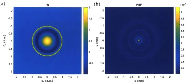
For instance, the polynomial Z4(q) introduces spherical aberration in the wavefront. Fig. 2-2 shows the W(q) function and the correspondent PSF(r) evaluated using MATLAB for
C2
= 2.2.1.2
Chromatic Aberrations
As previously anticipated the second category of aberration is chromatic aberrations. They are due to the fact that is impossible to generate a monochromatic beam. A beam generated by an electron gun is going to have a Gaussian energy distribution with energy spread AE. Electron lenses are going to exert the same force to each
(a)2W (b) PSF x101
(a)
2 -2 -2 2 -1.5 1.1. 5 .5 -1.8 -1 -1 1.8 1 1.4 -0.5 -0.5 1.2 . 0 0.5 0 0.5 0.5 0.8 0 1 1 0.6 1.5 -0.5 1.5 0.4 0.2 2 2 -2 -1.5 -1 -0.5 0 0.5 1 1.5 2 -2 -1.5 -1 -0.5 0 0.5 1 1.5 2 q. (a. u.) x (nm)Figure 2-2: Calculation of the phase factor and point spread function of a spheri-cally aberrated beam - The evaluation of the phase factor W(q) (a) and point spread function PSF(r) (b) for a beam affected by spherical aberration was performed using MATLAB. W(q) was calculated imposing C2 = 2, coefficient of the Zernike poly-nomial with n = 4 and m = 0. This is the polynomial responsible for spherical aberrations.
electron but electrons with different energies have different velocities, hence they are going to experience the deflection for a different time interval t. This characteristic entails that parallel rays of different energies are going to be focused at different positions. In particular electrons with lower energy are going to have a shorter focal length. The spot size due to these aberration can be evaluated with the following equation:
AE
dc = Cc a, (2.8)
E
where Cc is the coefficient of chromatic aberrations in m.
2.2
Electron Lenses
The main component necessary to build any electron optical system are electron lenses. These, as anticipated before, are elements which, on their azimuthal plane, impose a deflection to the electrons proportional to the distance from their optical axis. This deflection is a result of Lorentz force:
F= qE+qv x B. (2.9)
As can be seen from 2.9 this deflection can be generated by both an electric or a magnetic field. This property defines the two main categories of electron lenses: electrostatic and magnetic lenses. In the following, I am going to describe and simulate these components, characterizing their optical properties in terms of focusing power, image rotation and aberrations. Knowing these characteristics is crucial to design the different components comprising the multi-pass resonant cavity.
2.2.1
Electrostatic Lenses
Electrostatic lenses exploit the first term of the Lorentz force F = qE. They are comprised of stacking of rotationally symmetric electrodes with a round aperture, or bore, in the center. They exploit the electric field generated by these electrodes to deflect the electrons. In order to understand how they work it is necessary to solve the Laplace equation for a rotationally symmetric structure. In these conditions, if we know the potential on the optical axis, the resulting potential can be written as:[35, 21] ( ) r 2n a2nV(0, z) V(r, z) =
()
02 (2.10) n=o ( 2 2 (r2 > 02V(0, z) (r4') 4V(0, z) = V(0, z) -4
0z2 +I4
0z4 + (2.11) Which corresponds to the longitudinal and transverse electric fields:E (r, z)
DV(0, z)
(r2) a
3V(0,z) +...
(2.12)az
4
09z3 r 2 V(0, z) (.3 94V(0, z)Er(rz)
-)
0z2 - 16 z4+
(2.13)di-rection, instead the second one is responsible for the radial acceleration, hence the deflection. The first terms of the forces resulting from these field are:
&V(O, z) F,(r, z) = q Ez e 'v + ) . (2.14)
az
e &2 V(O, z) F,(r, z) q E, 2 z r +... (2.15)Since the longitudinal part is independent of r while the transverse one is linearly dependent on it, the deflection is going to be linearly dependent with r as well. Hence, this system behaves as a lens. In particular, the deflection is going to be dependent on the impulse FrAt. Therefore, it is going to be proportional to the curvature of the axial potential V(O, z) and to the time spent by the electron in that field, which
in turn depends on the initial velocity and the axial acceleration a, = Fz/me (that is proportional to the slope of the axial potential).
The curvature of the axial potential which determines the deflection can be con-trolled by modifying the potential of the different electrodes composing the lens stack. The curvature can be both positive or negative, which corresponds to a convergent (positive) or divergent (negative) lens effect, respectively. However, the only way to have a net divergent negative effect is to have a single electrode with a bore, and a flat counter-electrode, which corresponds to the case of an emitter or a mirror. Any higher number of electrodes is going to generate an overall positive lens effect. This characteristic comes from the fact that for any given couple of electrodes the electrons are going to experience two possible effects:
1. lower potential to higher potential: first a positive and then a negative curva-ture/lens effect (PN), together with an acceleration, so it is going to spend less time in the negative part, hence overall positive lens effect;
2. higher potential to lower potential: first a negative and then a positive curva-ture/lens effect (NP), together with a deceleration, so it is going to spend more time in the positive part, hence overall positive lens effect;
Typically when you want to design an electrostatic lens you want the electron before and after interacting with the lens to have the same energy. To achieve such a condition, you need the outermost electrodes to be at the same potential (usually the reference ground potential). To build such a system, the minimum number of electrodes is three. This kind of component is called a unipotential lens, or einzel lens. In the following, I am going to simulate an einzel lens using LorentzEM software modifying the different electrical and geometrical parameters, in order to study the dependence of the lens optical characteristics with them.
Fig. 2-3 (a,b) shows the simulation of the potential distribution of the einzel lens and the correspondent electron trajectories for an incoming beam with an energy of 5 keV, which is the energy that we intend to use in our first design of the multi-pass cavity. In this simulation the parameters used for the lens were:
1. electrode bore diameter D = 2 mm;
2. electrode thickness T = 2 mm; 3. electrode gap G = 2 mm.
The spherical aberration can be evaluated emitting a series of rays at different distances from the optical axis and measuring the resulting spot size after the in-teraction with the lens. The aberration coefficient can then be extracted using the relationship C, = 2, where a is the semi-angle of the marginal emitted ray.
The chromatic aberration instead can be evaluated emitting only marginal rays but with an energy spread AE. In this case, a spread of 2 eV was selected. Then, if the resulting spot size is measured after the interaction with the lens, the aberration coefficient can be evaluated from the relation Ce = .
Fig. 2-3 (c) and (d) shows the spot size due to spherical and chromatic aberration, respectively.
Fig. 2-4 shows the result of an analysis of the behavior of the spherical and chromatic aberration coefficients and the focal length of an einzel lens while varying the potential of the central electrode. The analysis was performed both using positive
(b)
E -1 -2 0--150 -100 -50 0 50 100 1 x (pm)(d)
-19. N -19.7- -19.8- -19.94--1 x (pm)Figure 2-3: Simulation of the potential distribution and ray-tracing of an einzel lens
-
(a) equipotential lines and (b) trajectories simulations, performed for a structure
with parameters D = T = G = 2 mm and E = 5 keV. The figure also shows the spot
size due to spherical (c) and chromatic (d) aberrations.
(a)
(C)
io -19.6 -19.7 -19.8 -19.9 N - -1 -1 0 x (pm) 2 1(a) (b) 102 . 50 102 50 -- -CS F -- Cs F 101- 40 10' 40 C E CE - 100 30 -30
C
8
a 10 - 20 C 10 -20 ) 011 , 4). @,10-1 .0 .0 M10-, 0 cc10-3 0 2 3 4 5 5 10 15 20 potential (kV) potential (kV)Figure 2-4: Simulation of the dependence of the optical characteristics of an einzel lens with its central electrode potential - The two graphs portray the result of the simulation showing the dependence of spherical and chromatic aberration coefficients
Cs and Cc and focal distance F, while varying the central electrode potential for a
negative potential (a) and positive potential (b) lenses.
and negative potentials on this electrode. In the first case, the resulting field generates a PNP lens effect while in the second case an NPN one. As we can see from the result, in the two cases, for the same focal length the aberration are comparable, but the lens with positive potential requires a much higher potential in absolute value respect to the negative potential one. This requirement is due to the fact that the positive lens accelerates the electrons so they are going to spend less time in the lens field. In both cases, as expected, the simulation shows a stronger focusing power for higher potential. Therefore, when possible, a negative potential lens is preferable since it reqiires using a less expensive voltage source.
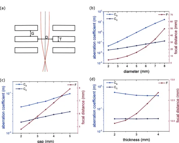
The next important step for designing a lens is to know the effect of the geomet-rical parameter of the lens itself on its optical properties. Fig. 2-5 shows the result of this characterization performed varying the electrodes diameter, gap, and thickness of a negative potential lens. As we can see from the result, a decrease of all these parameters brings a shorter focal distance. But while decreasing the diameter and the gap also decrease the aberrations, the thickness has a very small effect on the aberrations. Therefore, using an overall smaller lens is going to be beneficial. How-ever, we have also to consider the fact that a smaller lens is also going to be more
G IT CS F - -Cc 5 2 3 4 gap (mm) (d) 8 100 0 03 6V .2 5 10-2
Figure 2-5: Simulation of the dependence of the optical characteristics of an einzel
lens with its geometrical parameters
-
(a) Schematics of an einzel lens showing the
parameters: diameter D, gap G and thickness T. (b-d) portrays the result of the
simulation showing the dependence of spherical and chromatic aberration coefficients
Cs and Cc and focal distance F, while varying these parameters.
sensible to machining errors and alignment issues. Therefore, the optimal size has to
be selected keeping in mind the machining and assembling tolerances that you expect
to be able to achieve.
2.2.2
Magnetic Lenses
The second main category of electron lenses is magnetic lenses. These exploit the
second term of the Lorentz force F
=
qv x B. They are composed by a
rotation-ally symmetric structure comprised of a copper coil winded into a yoke of magnetic
material, such as iron. This yoke has a gap on the optical axis side. The two gap
(a) (b) Cs --10' 1001 10-1 10-2 E
8
a
0 70 EE
50 40 e 30 20 10 78 2 3 4 5 6 diameter (mm) (c) E 10-1 0 0 C 0 4) 10.-2 - C F - -Cc 13.0 12.5 (D U 12.0 0 4 2 thickness (mm) . . I -3 I ' IF-extremities, or pole pieces, concentrates the field in the optical axis region.
In order to understand how they work, it is necessary to solve the Laplace equation for a rotationally symmetric structure. In these conditions, if we know the field on the optical axis, the resulting off-axis longitudinal and transverse magnetic fields can be written as:[35]
B,(r, z)
=Bz(0, z)
-r
I
2'B(,
z)
(2.16)
4 Dz2
Br (r, Z) r oBz(0, z) r 303Bz(0, z) (2.17)
2
&z16
az3That in paraxial approximation gives the following equation for the transverse force:
192r(Z) 2B2(,)
Fr(r,
z) = m&1rZ2 -B(0,e=
r. (2.18)3z2 8E
Also in this case we can see that the transverse force is linearly dependent with r. Hence, this system behaves as a lens. It is worth noting that in this case the electron is not only focused, but it also follows a helical path, which introduces a rotation of the image plane. In particular, if we approximate the axial field with the following hat function with half-maximum width 2a:
B
0B,(0, z)
=o
2 .(2.19)1+
g7
Then, the resulting focal length and total image rotation can be approximated re-spectively as: 16mE 1 aE aB= 0
--
3
(2.20)
7re2aBO
I 2 > ewr I # aBOoc
, (2.21) 7/8mrE V5_where I is the total current passing through a section (I = Ni with N number of
(a)
(b)
20- 10-'El-I - -10-Om 4-1530 -100 -50 0 50 100 150 x (pm)Figure 2-6: Simulation of the magnetic field lines and ray-tracing of a magnetic lens
-
(a) magnetic field lines and (b) trajectories simulations, performed for a structure
with parameters I= 200 A, D
=G
=2 mm and E
=5 keV.
In the following, I am going to simulate a magnetic lens using LorentzEM software
modifying the different electrical and geometrical parameters, in order to study the
dependence of the lens optical characteristics with them.
Fig. 2-6 shows the geometry of the simulation of the magnetic field lines
distri-bution of the lens and the correspondent electron trajectories for an incoming beam
with an energy of 5 keV. In this simulation the parameters used for the lens were:
1. total section current I
=200 A;
2. bore diameter D = 2mm;
3. pole piece gap G
=2 mm.
The spherical aberration and chromatic aberrations are evaluated using the same
technique implemented in the simulation of the electrostatic lenses described earlier.
Fig. 2-7 shows the result of an analysis of the behavior of the spherical and
chromatic aberration coefficients and the focal length of a magnetic lens while varying
the total section current I, the bore diameter D and the pole piece gap G. As we can
see from the result, a higher focal distance can be achieved decreasing the current or
increasing the diameter or the gap but it also result in higher coefficients of spherical
and chromatic aberrations. In these simulations, I also evaluated the additional image
rotation with respect to that of a standard optical lens, which is ir. The results are
summarized in Table 2.2. The simulation showed that these values are practically independent on the geometry. They only have a linear dependence with the current, which is consistent with what found in Eq. 2.21.
Table 2.2: Image rotation dependence with the total section current I (A) <0 (deg) 100 15.06 200 30.12 300 45.18 400 60.27 500 75.36 600 90.40
2.3
Gated Mirror
In order to be able to build a linear cavity for electron, we need to develop components that can define a cavity, acting as mirrors when the electrons are inside the cavity. For a linear cavity, such components should also to be able to be gated so as to let the electron enters into the cavity and exit from it after having completed the required number of roundtrips. We are going to refer to this component as a gated mirror. The main working principle of a gated mirror is that when it has to act as a mirror it generates a potential in the beam path higher than that used to accelerate the electrons. Instead, when it is necessary to couple electrons in and out of the cavity this potential is lowered so to let the electrons pass through. This concept was first proposed for quantum electron microscopy by Kruit et al. in [16] where such an element is referred to as "barn door".
A design of a gated mirror for multi-pass microscopy has to take into account
some important factors:
1. it has to be operated faster than the roundtrip time of the electron in the cavity,
(b) 102 r 10 0 S10"1 0 10-2. . 2 G D 0 100 200 300 400 current (A) (d) 2 3 4 5 6 diameter (mm)
7 I ,
7 8 50 40 o( C ) cc 0 .4- CL) 20* C .0 0 101-0 10 101, 10-2 -0- c 2 3 4 5 6 7 8 gap (mm)Figure 2-7: Simulation of the dependence of the optical characteristics of a magnetic
lens with its total section current and geometrical parameters
-
(a) Schematics of
a magnetic lens showing the parameters: current I, diameter D and gap G.
(b-d) portrays the result of the simulation showing the dependence of spherical and
chromatic aberration coefficients
Cs
and Cc and focal distance F, while varying
these parameters.
(a) F. -6-cc - -Ce 60 5o E E 40 a 30 20 10 0 500 600 Cs - F c- 101-10 -10.-1 (c) C .0 10-2 50 40 E 30 a 20 10-in
has to be matched with an external pulse generator that has to be designed so to generate pulses of hundreds of volts at the ns timescale.
2. it has to minimize the effect of aberrations because they will build up with the number of roundtrips, disrupting the achievable resolution. To meet this speci-fication, the geometry of the gated mirror has to be accurately designed. As we will see in the following sections, a successful approach is to build aberration cor-rected mirrors. This technique is well established for standard electron mirrors
[30, 31, 32, 33] and its implementation for gated mirrors has been proposed,[34]
but not experimentally demonstrated yet.
In the following sections, some gated mirror designs are proposed and the gat-ing mechanism is verified through simulation. Then the possibility of upgradgat-ing the system to include an aberration-correction feature is discussed analyzing the charac-teristics of hyperbolic mirrors.
2.3.1
Design and Simulation of a Gated Mirror
The simplest gated mirror that we can design is comprised of a stacking of three electrodes insulated from each other, where a concentric aperture is drilled at the center of each of them. The central electrode has to be connected to a potential high enough so that at the center of the structure the potential is higher with respect to the electron energy. The external electrodes are instead grounded. The central electrode is also connected to a pulse generator which when activated lower the potential of the central electrode letting the electron pass through. The first simulation that was performed is a COMSOL RF time-dependent analysis of the gating mechanism in this base level structure.
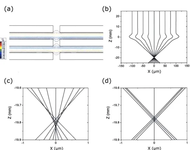
The COMSOL model for this simulation was built integrating electromagnetic waves, electrical circuit and charged particle tracing modules. Fig. 2-8 illustrates the COMSOL model that was implemented. The electrodes used in this model have gap G = 2 mm, bore diameter D = 1 mm and thickness T = 1 mm. The electron
Electrons
3 keV closed open
GND -2800-.2 -o 300 V -3700 V T =2ns- ..1 . -0.4 -0.2 0.0 0.2 0.4 0.6 0.6 1.0 Time (ns)
Figure 2-8: COMSOL model of a three-electrode gated mirror and potential at the
center of the structure
-
(a) TDTS model: mesh distribution and lumped ports of the
external pulse generator. The structure is matched with the external circuitry. (b)
The potential at the center of the structure.
A 300 V pulse 2 ns long with 100 ps rise time is then applied between the central
and the external electrodes which opens the gate. A scattering boundary condition
is applied to the external boundary of the model to avoid reflections. The device is
matched with the external circuitry using a parallel plate model for the characteristic
impedance (i.e. Z,,
=
Zoy). Fig. 2-8 (b) shows the simulation of the potential at
the center of the structure. When this potential goes below -3000 V the gate is open.
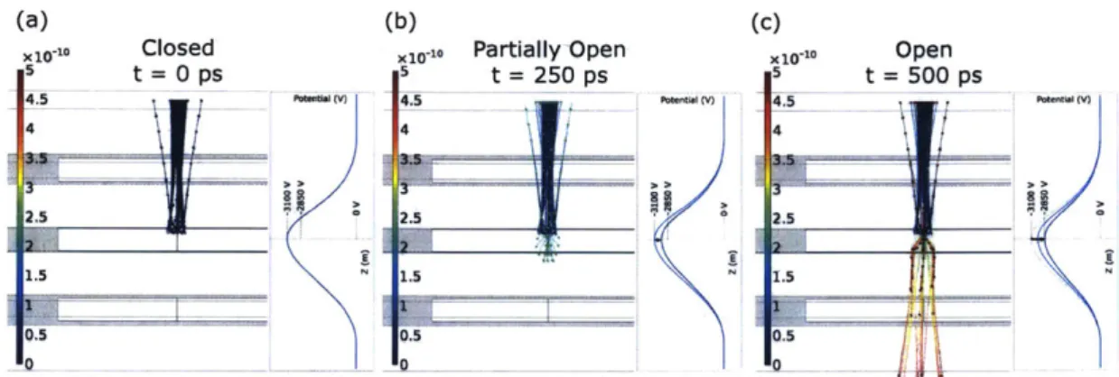
Fig. 2-9 illustrates the result of the time-dependent trajectory simulation of the
electron beam marginal rays. It is worth noting that the electron in-coupling while
lowering the potential has an effect on electron trajectories, therefore a very sharp
pulse and a pulsed electron source is required. In this way, the electrons will interact
only in the time period when the gate is fully closed or fully open. To avoid ringing or
minimizing its effect it is also important to operate the system when it is stabilized,
to match as well as possible the gate with the external circuitry and/or to adopt some
strategy of active compensation or feedback.
In order to have better control of the trajectories during resonance, in-coupling,
and out-coupling, it is beneficial to add two electrodes between the grounded external
electrodes and the central one, biased at an intermediate potential between the two.
Fig. 2-10 shows a possibility for this 5-electrode configuration. In this setup the
electrode parameters are: gap G
=
1.5 mm, thickness T
=
1 mm and bore diameter
(a) (b) (c)
X1-1 Closed x10 Partially Open XJO-10 Open
t= Ops 5 t= 250ps t= 500ps fawM4.5 P.WfM~CVM 4.5 Paw" M..Iiv
~
_ _ 4 4 4 2.5 2. 5 25 1.5 1.5P1 0.5 0.5Figure 2-9: COMSOL particle trajectories simulation during gating operation - (a-c) show the electron trajectories simulated using COMSOL particle tracing module at different simulated times.
D = 3 mm. In this figure, the results of the simulation are shown in terms of the equipotential lines in this structure, and the axial potential and the electron trajectories in closed and open configuration. The open configuration is achieved by applying a 150 V pulse to the central electrode.
It is not sufficient to simulate the DC operation of the gated mirror. An RF analysis it is also necessary in order to establish if this structure can be operated at the required speed or if the capacitance of the electrodes is going to prevent the high-speed operation. To do so a 3D COMSOL model was built, imagining a possible implementation of the structure. Fig. 2-11 (a) shows a cross-section of the simulated geometry, where the potential pulse is applied with a matched coaxial cable connected with a pin going to the central electrode and the grounded external conductor is connected to the external shielding of the structure, that is also connected to the two external electrodes. The pulse is applied from the left side of this structure as can be seen from the picture. In this structure, the electrode can be isolated from one another and the whole system can be held together using insulating spacers of cylindrical or spherical shape. Fig. 2-11 (b) is a simulation of the axial potential at the center of the core electrode. As can be seen from this simulation, with this design, a pulse of 100 V have a time constant of few ns. Since the electron pulse has to interact with a potential as stable as possible, a good choice would be to time
(b)
10-5. 0-NV
-325
-V-
-VM3 =-3250 V . , . . . , . -100 -50 0 X (pm) 50 100-5--3.5
(d)
N 150 10.0- 7.5- 5.0- 2.5- 0.0- -2.5- -5.0- -7.5--10.0 -3.0 -2.5 -2.0 -1.5 -1.0 potential (kV) -150 -100 -50 -0.5 0.0 50 100 150 X (pm)Figure 2-10: DC ray-tracing simulation of a five-electrode gated mirror in open and
closed condition
-
(a) Geometry and potential distribution of the electron gated
mir-ror. The multi-colored lines indicate equipotential surfaces. The potential used for
the simulation are the following:
VM1 = VM5 =0 V,
VM2 = VM4 =-2490
V, VM3-
-3250 V. The applied pulse is of 150 V. The geometrical parameters used are: gap
G = 1.5 mm, thickness T = 1 mm and bore diameter D = 3mm. (b) Axial potential
at the electron gate in open and closed configuration. (c) Raytracing simulation in
closed condition.(c) Raytracing simulation in open condition.
(a)
(c)
N xE3 -0411 .0.616 .2MI-2.274
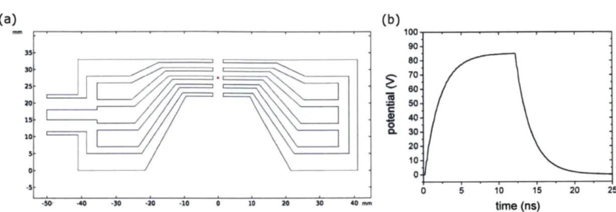
-241 2666 -26656 -3.102 10.0. 7.5- 5.0- 2.5- 0.0- -2.5- -5.0-VM3 = -3100 V -open dosed -7.5 -150(a) (b) 100 90 80 30.7 25- 70. 30 :50-1is. 40-10 .30' 20-10 0 0 -0 10 1,5 20 25 . -40 .30 40 .10 0 10 30 30 """ time (ns)
Figure 2-11: Geometry of the COMSOL model of the gated mirror prototype and simulation of the central potential - (a) illustrates the simulated geometry with the input for the electrical connection done with a coaxial cable on the right. (b) shows the simulated axial potential at the center of the middle electrode. This is evaluated doing a line integral of the field from the field free region. The point at which the potential is evaluated is highlighted in red in (a).
the electron pulse to reach the gate in the time frame 9-12 ns from when the pulse is generated. After this moment the system needs other 10 ns to restore the closed configuration. Therefore, the cavity has to be long enough so that the time required for an electron to do a roundtrip is more than 10 ns. If this constraint were to be too limiting, alternatively, the design can be modified so as to have a smaller device, hence a smaller capacitance and a smaller time constant. This modification can be done maintaining the same geometry close to the optical axis so that the optical properties would not be affected. Here, this particular design was used because these are the dimensions that were used to build the first prototype, which will be described in the next section.
Fig. 2-12 instead illustrates the field distribution inside the structure at different times when the pulse is applied. The field is shown at 2 ns, 4 ns, 8 ns, and 16 ns. The potential is applied from external circuitry which is matched to the coaxial cable connected to the central electrode and the external shielding. The coaxial cable has an internal conductor of diameter d = 3 mm and an external conductor of diameter d =
10 mm, hence its characteristic impedance is Zo = 1 log(D/d) = 72.2 Q. Therefore the external circuit is simulated using its Thevenin's equivalent: a pulse generator and a 72.2 Q resistor.