Design Automation and Analysis of Three-Dimensional
Integrated Circuits
by
Shamik Das
S.B. E.E., Massachusetts Institute of Technology (2000)
S.B. Mathematics, Massachusetts Institute of Technology (2000)
M.Eng. E.E.C.S., Massachusetts Institute of Technology (2000)
Submitted to the Department of Electrical Engineering and Computer Science
in partial fulfillment of the requirements for the degree of
Doctor of Philosophy
at the
MASSACHUSETTS INSTITUTE OF TECHNOLOGY
May 2004@
Massachusetts Institute of Technology 2004. All rights reserved.
Author...
Department of Electrical Engineering and Computer Science
May 1, 2004
C ertified by ...
.-.
Rtafael Reif
Associate Department Head and Professor of Electrical Engineering and Computer
Science
Thesis Supervisor
C ertified b y ... ...
...
Anantha P. Chandrakasan
Professor of Electrical Engineering and Computer Science
Thesis Supervisor
Accepted by ...
thur C. Smith
Chairman, Department Committee on Graduate Students
MASSACHUSETTS 1iTTUT OF TECHNOLOGY
Design Automation and Analysis of Three-Dimensional Integrated
Circuits
by Shamik Das
Submitted to the Department of Electrical Engineering and Computer Science on May 14, 2004, in partial fulfillment of the
requirements for the degree of Doctor of Philosophy
Abstract
This dissertation concerns the design of circuits and systems for an emerging technology known as three-dimensional integration. By stacking individual components, dice, or whole wafers using a high-density electromechanical interconnect, three-dimensional integration can achieve scalability and performance exceeding that of conventional fabrication technolo-gies.
There are two main contributions of this thesis. The first is a computer-aided design flow for the digital components of a three-dimensional integrated circuit (3-D IC). This flow primarily consists of two software tools: PR3D, a placement and routing tool for custom 3-D ICs based on standard cells, and 3-D Magic, a tool for designing, editing, and testing physical layout characteristics of 3-D ICs. The second contribution of this thesis is a performance analysis of the digital components of 3-D ICs. We use the above tools to determine the extent to which 3-D integration can improve timing, energy, and thermal performance. In doing so, we verify the estimates of stochastic computational models for 3-D IC interconnects and find that the models predict the optimal 3-D wire length to within 20% accuracy. We expand upon this analysis by examining how 3-D technology factors affect the optimal wire length that can be obtained. Our ultimate analysis extends this work by directly considering timing and energy in 3-D ICs. In all cases we find that significant performance improvements are possible. In contrast, thermal performance is expected to worsen with the use of 3-D integration. We examine precisely how thermal behavior scales in 3-D integration and determine quantitatively how the temperature may be controlled during the circuit placement process. We also show how advanced packaging technologies may be leveraged to maintain acceptable die temperatures in 3-D ICs.
Finally, we explore two issues for the future of 3-D integration. We determine how technology scaling impacts the effect of 3-D integration on circuit performance. We also consider how to improve the performance of digital components in a mixed-signal 3-D integrated circuit. We conclude with a look towards future 3-D IC design tools.
Thesis Supervisor: Rafael Reif
Title: Associate Department Head and Professor of Electrical Engineering and Computer Science
Thesis Supervisor: Anantha P. Chandrakasan
To my mother, father, and sister and
Acknowledgments
This dissertation would not have been possible without the love and support of my family.
My mother, father, and sister have cared for me and instilled in me a sense of purpose that
goes beyond mere circuits. For their dedication and inspiration, I will be forever grateful. I am honored to have been the student of two professors, Rafael Reif and Anantha Chandrakasan, during my graduate tenure at MIT. Their mentorship of my research has been outstanding, and I could not have asked for better guides. Both advisors have given me a wealth of perspective, insight, and motivation.
Several other professors at MIT have been instrumental in my development as a scientist and engineer. I would like to thank Duane Boning for serving on my thesis committee and for the guidance he has ably provided in this capacity. John Kassakian has been an exceptional graduate counselor by keeping me on track with respect to degree requirements and giving me valuable career advice.
It is my personal (though not unique) belief that every student should participate in teaching, and I have had the fortunate opportunity to learn from a master, Professor Amar
G. Bose. The experience of being one of his teaching assistants has fundamentally shaped
my views on education, engineering, and communication, not to mention politics, society, religion, and the weather. For this alone, my graduate career has been worthwhile.
I would also like to thank all the members, current and former, of my two research groups. For their collaboration on this research effort and others, and for their compan-ionship and advice, I appreciate them tremendously. My life as a graduate student, on a daily basis and at conferences, presentations, and reviews, was all the more enriched by sharing it with such colleagues. The broader community of people at the Microsystems Technology Laboratories at MIT also deserves much appreciation. A special thanks goes out to Susan Kaufman and Margaret Flaherty for their tireless administrative efforts, as well as for keeping me in tune with the world outside of work.
Several people have made specific contributions that deserve mention here. Professor Arifur Rahman of Polytechnic University developed a model that forms the basis for part of the work in this dissertation. During the few months that we were colleagues at MIT and in subsequent years, he has provided valuable guidance both in my attempts to ana-lyze and validate his model and in my career in general. I would also like to thank MIT
students Elizabeth Basha, Katie Butler, Patrick Griffin, Wei-Han Huang, and Vivian Lei for volunteering to test one of the design tools I developed for this dissertation, as well as for agreeing to let me publish their results.
My time at MIT has not been occupied solely by the analysis of integrated circuits.
Along the way, I have become blessed with many friends. My four years at Zeta Beta Tau fraternity as an undergraduate have provided me with close friendships that continue to this day. I also would not have maintained my sanity, health, and motivation were it not for the sport of ultimate and the friendships I have formed through it. I would like to thank my teammates on the MIT Ultimate Team for the experience, though I must acknowledge that my two remaining years of college eligibility provided a strong disincentive to the completion of this dissertation.
Finally, this dissertation would not exist were it not for my fiancee, Anne. She has been a constant companion throughout my graduate years, providing compassion and encour-agement, as well as bringing formidable literary skills to bear on drafts of this document. I can only hope that over our life together, I can return the love she has already given me.
Contents
1 Introduction 23
1.1 Motivation of this Work . . . . 23
1.1.1 Scaling Limitations of Conventional Integration Technology . . . . . 23
1.1.2 The Potential of Three-Dimensional Integration . . . . 25
1.2 Three-Dimensional Integration Technology . . . . 26
1.2.1 Packaging Methods . . . . 27
1.2.2 Monolithic Approaches . . . . 29
1.2.3 Sample Process Flow: Copper Wafer Bonding . . . . 31
1.3 Design Tradeoffs Associated with the 3-D Integration Process Flow . . . . . 33
1.3.1 D igital ICs . . . . 33
1.3.2 Analog/Mixed-Signal ICs . . . . 33
1.4 Overview of Previous Work . . . . 34
1.4.1 Stochastic Modeling of 3-D ICs . . . . 34
1.4.2 Architectural Investigation . . . . 34
1.4.3 Unresolved Problems . . . . 35
1.5 Contributions of this Dissertation . . . . 36
2 Design Tools for Three-Dimensional Integrated Circuits 39 2.1 O verview . . . . 39 2.2 Logic Synthesis . . . . 40 2.3 Floorplanning . . . . 42 2.4 Placem ent . . . . 43 2.4.1 Global Placement . . . .. . . . .. 44 2.4.2 Detailed Placement . . . . 44
2.4.3 2.4.4 2.4.5 2.4.6 2.5 Routin 2.5.1 2.5.2 2.6 Layout 2.7 PR3D: 2.7.1 2.7.2 2.7.3 2.8 3-D Ma 2.8.1 2.8.2 2.8.3 2.8.4 2.9 Summa
Placement Algorithm: Simulated Annealing Placement Algorithm: Quadratic Placement Placement Algorithm: Partitioning . . . . . Detailed Placement Algorithms . . . .
g . . . .
Hierarchical Approach . . . . Global Maze Router . . . .
Gloal. az. Roe...
The Placement and Routing Tool . . . .
3-D Standard-Cell Placement Algorithm . . 3-D Global Routing . . . .
Comparison of PR3D with Other Tools . . gic: The Layout Editor . . . . User Interface Design . . . . Circuit Issues . . . . Data Representation . . . . Sample Layouts Using 3-D Magic . . . .
ry . . . . 44 46 48 50 51 52 53 53 54 56 58 59 60 60 61 63 65 69
3 Wire-Length Performance of 3-D Integrated Circuits 3.1 Previous Work on 3-D IC Analysis . . . .
3.2 The Rahman Model . . . .
3.2.1 Derivation . . . .
3.2.2 Adaptations for Standard-Cell Circuits . . . . . 3.3 Analysis of 3-D ICs: Model vs. PR3D . . . . 3.3.1 Calibration . . . .
3.3.2 Verification of the Rahman Model . . . .
3.3.3 Further Analyses via PR3D . . . .
71 71 74 74 76 78 78 78 84 3.4 Summary . . . . 88
4 Performance Characteristics of 3-D ICs
4.1 O verview . . . .
4.2 Tool Adaptations for Performance-Driven Design . . . .
91
91 93
4.3 Methodology and Circuits Under Test . . . . 4.4 Timing Characteristics of 3-D ICs . . . .
4.5 Energy Characteristics of 3-D ICs . . . . 4.5.1 Energy Performance of the Conventional Circuits Under Test 4.5.2 Energy Optimization in 3-D . . . . 4.6 Energy-Delay Product . . . . 4.7 Sum m ary . . . .
5 3-D IC Thermal Management and Optimization
5.1 M otivation . . . . 5.2 First-Order Model for Die Temperature in 3-D ICs . . . . .
5.3 Placement-Based Optimization of Thermal Characteristics . 5.4 Thermal Characteristics of 3-D ICs . . . .
5.5 Active Cooling Using Microchannels . . . .
5.5.1 First-Order Model . . . .
5.5.2 Modifications to the Thermal Algorithms . . . .
5.5.3 Placement-Based Analysis . . . . 5.6 Sum m ary . . . . 107 . . . . . 107 . . . . . 109 .. .. 111 . . . . . 112 . . . . . 118 . . . . . 120 . . . . . 122 .123 . . . . . 127
6 Future Considerations for 3-D Integration 6.1 O verview . . . . 6.2 Predictive Technology Models: Impact of 3-D Integration in Future Technology G enerations . . . . 6.2.1 M otivation . . . . 6.2.2 Fixed-Chip Scaling . . . . 6.2.3 3-D Integration of the Projected "Largest Chip" . . . .. 6.3 Opportunities for Mixed-Signal 3-D Integration . . . . 6.3.1 O verview . . . . 6.3.2 Optimization for Digital Performance in Mixed-Signal Systems . . . 6.3.3 Optimization of the Digital Noise Impact on Analog/RF Subsystems 6.4 Architecture for a Design Flow for Mixed-Signal 3-D ICs . . . . 6.5 Sum m ary . . . .. 95 96 . . . 98 . . . 98 . . . 100 . . . 104 . . . 104 131 131 131 131 132 137 139 139 141 143 146 149
7 Conclusion
7.1 Summary of Research Results
7.2 Directions for Future Work . . .
7.2.1 Technology Research . . .
7.2.2 CAD Tools . . . .
7.2.3 Circuit Design . . . .
A Usage Information for the 3-D Design Tools
A.1 PR3D: The Placement and Routing Tool . . . . A.1.1 Platform Support . . . .
A .1.2 U sage . . . .
A.1.3 File Formats . . . .
A.2 3-D Magic: The Layout Editor . . . . A.2.1 Platform Support . . . .
A .2.2 U sage . . . .
A.2.3 Commands . . . .
A.2.4 Extensions to the Magic Technology File Format
. . . . . . . . . . . . . . . . . . . . 151 151 153 153 154 155 157 157 157 157 159 161 161 161 162 163 . . . . . . . .
List of Figures
1-1 Projected inverter F04 and 1-mm interconnect delays for various technology nodes. ... ... 24 1-2 Schematic of a 3-D integrated circuit with interleaved device layers and
inter-layer interconnects. . . . . 25 1-3 Wire-length distribution of a typical circuit as a function of number of device
layers used. . . . . 26
1-4 (a) Vertical multi-chip module (MCM-V) schematic. (b) Schematic of flip-chip bonded circuit. . . . . 27 1-5 Vertical multi-chip module (MCM-V) showing inter-layer interconnect
back-plane. Left: schematic; right: package photo (reprinted from [1]). . . . . 28 1-6 Flip-chip package with solder-bump interconnect (reprinted from [2]). . . . 29 1-7 Wafer-bonded structure with two device layers and copper interconnect
in-terface. (Figure courtesy A. Fan, MIT.) . . . . 30 1-8 Multiple-wafer structure using oxide as the bonding interface. The
inter-wafer interconnects are formed after bonding. (Figure courtesy MIT Lincoln Laboratory.) . . . . 31 1-9 Handle-wafer attachment, grindback, via formation, and copper patterning
steps of the wafer bonding process. (Figure courtesy A. Fan.) . . . . 31 1-10 Thermocompression and handle release steps of the wafer bonding process.
(Figure courtesy A. Fan.) . . . . 32
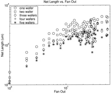
2-1 Simplified flowchart for the automated design of 2-D and 3-D digital inte-grated circuits. . . . . 40 2-2 Wire length as a function of fan-out for a benchmark circuit. . . . . 41
2-4 Typical simulated-annealing sequence for a simple network at initial, inter-m ediate, and final stages. . . . . 45
2-5 Single-net example of the hierarchical routing procedure. Routing proceeds from stage (a) to (f) by recursive partitioning . . . . 52 2-6 Partitioning strategy where plane assignment is done first in order to
mini-mize the number of inter-plane vias. . . . . 56 2-7 Partitioning strategy where plane assignment is done by considering aspect
ratio in order to minimize total wire length. . . . . 56 2-8 For small inter-wafer via sizes, we permit same-row interconnects to be split
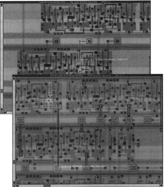
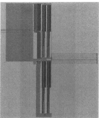
among multiple wafers. For large inter-wafer via sizes, we partition into wafers before reaching the single-row block size. . . . . 57 2-9 Screen shot of 3-D Magic exhibiting a two-wafer circuit layout. . . . . 62
2-10 Bonded stack of CellDef structures with up and down pointers for front-side and back-side bonding contacts and prev and next pointers for stack traversal. 64 2-11 Bottom wafer of a two-wafer class-E amplifier designed by Wei-Han Huang
and V ivian Lei. . . . . 65
2-12 Top wafer of a two-wafer class-E amplifier designed by Wei-Han Huang and V ivian Lei. . . . . 66 2-13 Power efficiency of the 1.9 GHz amplifier in 2-D (o) and 3-D (*)
implemen-tations. Total power is given in third curve (A). . . . . 67
2-14 Crosstalk on adjacent multiplexer lines in the selector subcircuit of the 1.9 GHz amplifier, in 2-D (A) and 3-D (*) cases, as a function of separation distance. . . . . 67 2-15 Block diagram for a four-bit ADC designed by Elizabeth Basha, Katie Butler,
and Patrick Griffin. . . . . 68
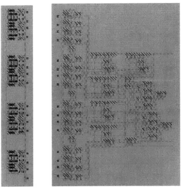
2-16 Top wafer (left) and bottom wafer (right) of the two-wafer ADC designed by
Elizabeth Basha, Katie Butler, and Patrick Griffin. . . . . 68 2-17 Signal-to-noise-and-distortion ratio (SNDR) for 2-D and 3-D
implementa-tions of the AD C . . . . . 69
3-2 Schematic representation of the derivation of occupancy distribution: Na =
1 is the logic gate in question, N, is the number of target logic gates at Manhattan distance 1 gate pitches, and Nb is the number of logic gates in between. to, ty, and t, are the gate width, height, and inter-layer thickness, respectively, in micrometers. (Figure courtesy A. Rahman.) . . . . 74
3-3 Predicted wire-length distribution for the ibm14 benchmark circuit with inter-layer pitch t, of 1 micrometer . . . . . 79
3-4 Placed wire-length distribution for the ibm14 benchmark circuit with inter-layer pitch tz of 1 micrometer . . . . 80
3-5 Predicted vs. placed and routed wire lengths of the average benchmark circuit. Wire length is given relative to the 2-D placed wire length. Inter-layer pitch t, is 1 micrometer. . . . . 81 3-6 Predicted vs. placed and routed wire lengths of the average benchmark
circuit. Wire length is normalized to exhibit the percentage reduction due to
3-D integration. Inter-layer pitch t, is 1 micrometer. . . . . 81 3-7 Predicted vs. placed and routed wire lengths of the average benchmark
circuit. Wire length is given relative to the 2-D placed wire length. Inter-layer pitch tz is 250 micrometers. . . . . 82 3-8 Predicted vs. placed and routed wire lengths of the average benchmark
circuit. Wire length is normalized to exhibit the percentage reduction due to
3-D integration. Inter-layer pitch t, is 250 micrometers. . . . . 82 3-9 Predicted percentage of interconnects that span multiple device layers,
com-pared with placement and routing data for tz = 1 and t, = 250. . . . . 84
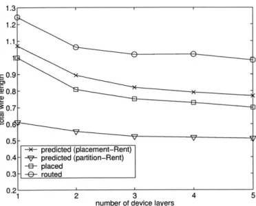
3-10 Total wire length (as a function of number of device layers) for various
inter-layer via capacitances, obtained from placement. Total wire length is min-imized by the placement tool. Via cost is the via capacitance expressed relative to the capacitance of one micrometer of metal wire. . . . . 85 3-11 Total wire length (as a function of number of device layers) for various
inter-layer via capacitances, obtained from routing. Total wire length is minimized
by the routing tool. Via cost is the via capacitance expressed relative to the
3-12 Total wire length (as a function of number of device layers) for various
inter-layer via capacitances, obtained from placement. The number of inter-inter-layer vias is minimized by the placement tool. Via cost is the via capacitance
expressed relative to the capacitance of one micrometer of metal wire. . . . 86
3-13 Total wire length (as a function of number of device layers) for various inter-layer via capacitances, obtained from routing. The number of inter-inter-layer vias is minimized by the routing tool. Via cost is the via capacitance expressed relative to the capacitance of one micrometer of metal wire. . . . . 88
3-14 Length of the longest wire (as a function of number of device layers) for various inter-layer via capacitances. Total wire length is minimized by the placement tool. Via cost is the via capacitance expressed relative to the capacitance of one micrometer of metal wire. . . . . 89
3-15 Length of the longest wire (as a function of number of device layers) for vari-ous inter-layer via capacitances. The number of inter-layer vias is minimized by the placement tool. Via cost is the via capacitance expressed relative to the capacitance of one micrometer of metal wire. . . . . 89
3-16 Total wire length (as a function of number of device layers) of the ibm03 benchmark circuit, using vias vs. using flip-chip solder bumps for the inter-layer interconnect. . . . . 90
4-1 Power consumption for a high-performance microprocessor at various technology generations... ... 92
4-2 Delay model for gates and wires. . . . . 95
4-3 Cycle time of an FFT datapath using various placement modes. . . . . 96
4-4 Cycle time of a DES implementation using various placement modes. ... 97
4-5 Cycle time of a 64-bit MAC using various placement modes. . . . . 97
4-6 Energy consumption of an FFT datapath in optimized vs. timing-constrained placement. . . . . 98
4-7 Energy consumption of a DES chip in timing-optimized vs. timing-constrained placem ent. . . . . 99
4-8 Energy consumption of a multiplier-accumulator chip in timing-optimized vs. timing-constrained placement. . . . . 100
4-9 Energy consumption of the FFT datapath vs. number of wafers used for placem ent. . . . . 100
4-10 Energy consumption of the DES chip vs. number of wafers used for placement. 101 4-11 Energy consumption of the 64-bit MAC vs. number of wafers used for
place-ment. ... ... 101
4-12 Energy-delay product for the FFT datapath vs. number of wafers used for placem ent. . . . . 102 4-13 Energy-delay product for the DES chip vs. number of wafers used for
place-ment. ... ... 103
4-14 Energy-delay product for the 64-bit MAC vs. number of wafers used for placem ent. . . . . 103
4-15 Wire energy-delay product for the FFT datapath vs. number of wafers used for placem ent. . . . . 104 4-16 Wire energy-delay product for the DES chip vs. number of wafers used for
placem ent. . . . . 105
4-17 Wire energy-delay product for the 64-bit MAC chip vs. number of wafers used for placem ent. . . . . 105
5-1 Minimum required heat sink thermal resistance by technology generation, based on ITRS projections for microprocessor size and power dissipation. The desired maximum die temperature is 1000C. . . . . 108 5-2 Temperature of the uppermost die in a 3-D stack, assuming 50 W power
dissipation, 2 sq. cm. total circuit area, and 25'C ambient temperature. . . 111
5-3 Celsius die temperature of the top wafer of a three-wafer placement of the FFT datapath. . . . . 113
5-4 Energy distribution of the top wafer of a three-wafer placement of the FFT datapath. . . . . 113 5-5 Die temperature of the FFT datapath vs. number of wafers (fixed-die case). 114
5-6 Absolute temperature differential of the FFT datapath vs. number of wafers (fixed-die case). . . . . . . 114
5-7 Average-temperature z-axis differential of the FFT datapath vs. number of wafers (fixed-die case). . . . . 115
5-8 Die temperature of the FFT datapath vs. number of wafers (scaled-die case). 115
5-9 Absolute temperature differential of the FFT datapath vs. number of wafers (scaled-die case). . . . . 116 5-10 Average-temperature z-axis differential of the FFT datapath vs. number of
wafers (scaled-die case). . . . . 116 5-11 Interconnect energy dissipation of the FFT datapath vs. number of wafers
in energy-optimized and gradient-optimized cases. . . . . 117 5-12 Minimum required heat sink thermal resistance by technology generation,
based on ITRS projections for microprocessor size and power dissipation and 3-D performance-scaling data from this work. The desired maximum uppermost-die temperature is 1000C. . . . .
118 5-13 Wafer-bonded structure with the addition of fluid microchannels for cooling
(c.f. Figure 1-7). . . . . 120 5-14 Microchannel with fluid flow in the positive x direction, power flow profile
P(x), and fluid temperature Teh(x), in an ambient solid temperature Tdie. . 121
5-15 Celsius die temperature prediction for the 2-D FFT, with microchannel heat
sink, as a function of channel cross-sectional dimension and fluid velocity. . 124
5-16 Head loss in p.s.i. for the FFT microchannels as a function of channel
cross-sectional dimension and fluid velocity. . . . . 125 5-17 Die temperature of the FFT datapath vs. number of wafers (microchannel
case). . . . . 126 5-18 Absolute temperature differential of the FFT datapath vs. number of wafers
(m icrochannel case). . . . . 126 5-19 Average-temperature z-axis differential of the FFT datapath vs. number of
wafers (microchannel case). . . . . 127 5-20 Celsius die temperature as a function of the number of wafers and the number
of microchannels used. The 2-D version of this chip dissipates 50 W and has dimensions 1.5 cm x 1.5 cm. The microchannels are 50 jim in effective diameter and the water flow is 25 cm/s at 25'C at the inlet. . . . . 128 6-1 Cycle time of the 64-bit MAC implemented in a 35 nm 3-D technology with
6-2 Energy consumption of the 64-bit MAC implemented in a 35 nm 3-D technology w ith via scaling. . . . . 134
6-3 Energy-delay product of the 64-bit MAC implemented in a 35 nm 3-D technology w ith via scaling. . . . . 134 6-4 Interconnect energy-delay product of the 64-bit MAC implemented in a 35
nm 3-D technology with via scaling. . . . . 135 6-5 Cycle time of the 64-bit MAC implemented in a 35 nm 3-D technology
with-out via scaling. . . . . 135 6-6 Energy consumption of the 64-bit MAC implemented in a 35 nm 3-D technology
without via scaling. . . . . 136 6-7 Energy-delay product of the 64-bit MAC implemented in a 35 nm 3-D technology
without via scaling. . . . . 136 6-8 Interconnect energy-delay product of the 64-bit MAC implemented in a 35
nm 3-D technology without via scaling. . . . . 137 6-9 Predicted CPU frequency for several technology generations using one to five
device layers for implementation. . . . . 138 6-10 Substrate noise spectrum for a 1 GHz Pentium@ 4 microprocessor operating
at 1.5 V supply and dissipating 15 Watts (reprinted from [3]). . . . . 140
6-11 Placement of a 3-D mixed-signal system. In (a) each module is targeted for a
separate wafer. In (b) non-critical digital components are placed on memory or analog wafers in order to reduce wasted silicon. . . . . 140
6-12 Three implementations of a mixed-signal circuit. Top left: single wafer; top
right: two wafers with digital circuitry isolated to bottom wafer; bottom: two wafers with equal footprint. . . . . 142
6-13 Cycle time of the FFT datapath in a mixed-signal circuit in four placement
modes: (1) single-die, (2) two dice with separation of analog and digital systems, (3) two dice of equal area with excess digital on the analog die, (4) same as (3) but with larger vias. . . . . 142 6-14 Interconnect energy dissipation of the FFT datapath in a mixed-signal circuit
in four placement modes: (1) single-die, (2) two dice with separation of analog and digital systems, (3) two dice of equal area with excess digital on the analog die, (4) same as (3) but with larger vias. . . . . 143
6-15 Cycle time of the 64-bit MAC in a mixed-signal circuit in four placement
modes: (1) single-die, (2) two dice with separation of analog and digital systems, (3) two dice of equal area with excess digital on the analog die, (4) same as (3) but with larger vias. . . . . 144
6-16 Interconnect energy dissipation of the 64-bit MAC in a mixed-signal circuit in
four placement modes: (1) single-die, (2) two dice with separation of analog and digital systems, (3) two dice of equal area with excess digital on the analog die, (4) same as (3) but with larger vias. . . . . 144
6-17 Cycle time of the 64-bit MAC two-wafer, equal-area, mixed-signal
implemen-tation. (1) and (3) are cases where the clock is distributed over both wafers; (2) and (4) are cases where the clock is restricted to the bottom wafer. (1) and (2) are cases where the inter-wafer vias are small; (3) and (4) represent larger inter-wafer vias. . . . . 145
6-18 Interconnect energy dissipation of the 64-bit MAC two-wafer, equal-area,
mixed-signal implementation. (1) and (3) are cases where the clock is dis-tributed over both wafers; (2) and (4) are cases where the clock is restricted to the bottom wafer. (1) and (2) are cases where the inter-wafer vias are small; (3) and (4) represent larger inter-wafer vias. . . . . 146
6-19 Digital vs. proposed mixed-signal design flow paradigms . . . . 146
List of Tables
1.1 ITRS predictions for circuit performance. . . . . 24 1.2 ITRS predictions for wires in integrated circuits. . . . . 24 2.1 Algorithm 3DPLACE for multi-wafer placement using min-cut partitioning. 55
2.2 Effective number of bits (ENOB) for 2-D and 3-D implementations of the ADC... ... 67
3.1 Performance of our placer and other state-of-the-art placers on the
IBM-PLACE 2.0 circuit benchmark set. Wire lengths are in meters. . . . . 78 3.2 Cells of the ISPD '98 benchmark suite used in this study. . . . . 79 3.3 Absolute prediction error relative to placed wire length as a function of
num-ber of device layers and inter-layer thickness. . . . . 83
3.4 Absolute prediction error relative to routed wire length as a function of num-ber of device layers and inter-layer thickness. . . . . 83 3.5 Placement and routing data for the ISPD '98 benchmark suite. Wire lengths
are in tm. Percentages are reductions relative to the one-wafer case. ... 87 4.1 Relevant parameters for the circuits in this study. . . . . 96 6.1 Properties of devices and mid-level interconnect in 180 nm and 35 nm
Chapter 1
Introduction
1.1
Motivation of this Work
1.1.1
Scaling Limitations of Conventional Integration Technology
For several decades, integrated circuits have profoundly impacted our everyday lives. In order to sustain this impact, it is widely expected that the decades-long trend of exponential growth in circuit performance and functionality must be sustained as well. However, the path to continued growth contains many obstacles.
The International Technology Roadmap for Semiconductors (ITRS) provides a detailed plan for achieving this growth [5]. In Table 1.1, we see specifically what is desired of circuit designers and manufacturers. The performance demands listed in the table must be met both by increasing transistor device capabilities and by improving the performance of the wires that connect these devices.
While device scaling is by no means a solved problem, the performance of scaled devices is at least understood to increase as desired. In contrast, the performance of scaled wires does not increase similarly. Table 1.2 shows the degree to which interconnect must be shrunk merely to meet functionality demands. However, at this level of scaling, worst-case and even average-case interconnect performance decreases with each generation.
Figure 1-1 illustrates the problem. A fan-out-of-four (F04) inverter (i.e. an inverter that is used to drive four identical inverters) scales with increasing technology generations, such that the signal delay through an F04 inverter is roughly proportional to the node length. However, the delay through a representative 1 mm wire increases exponentially from
gen-technology node (nm) 180 130 90 65 45 35 microprocessor
transistors/chip 21 76 226 453 773 1,227 (millions)
on-chip local clock
frequency (GHz) 1.25 2.1 4.171 9.285 15.079 20.065 chip-to-board clock frequency (GHz) 1.2 1.6 2.5 4.883 9.536 14.901 power supply (V) 1.8 1.5 1.2 1.1 1.0 0.9 CPU power (W) 90 130 158 189 218 240 chip size (mm2) at introduction 280 280 280 280 280 280 in production 140 140 140 140 140 140
Table 1.1: ITRS predictions for circuit performance.
technology node (nm) 180 130 90 65 45 35
number of metal layers 6-7 7-9 10-14 11-15 12-16 12-16 minimum metal pitch (nm) 360 300 214 152 108 84 effective resistivity (RQ -cm) 2.2 2.2 2.2 2.2 2.2 2.2 effective inter-layer
dielectric constant 3.5-4.0 3.3-3.6 3.1-3.6 2.7-3.0 2.3-2.6 2.3-2.6 Table 1.2: ITRS predictions for wires in integrated circuits.
Gate and Interconnect Delays by Generation Annfl 350 300 250 t200 150 100 501 -9- inverter F04 delay -G- 1 mm interconnect delay 3545 90 6 13 o35 45 65 90 130 technology node (nm) 180
Figure 1-1: Projected inverter F04 and 1-mm interconnect delays for nodes.
device layer 3
inter-layer interconnects
device layer 2
device layer I
Figure 1-2: Schematic of a 3-D integrated circuit with interleaved device layers and inter-layer interconnects.
eration to generation, due to the increased resistance from scaling down the cross-sectional area of the wire. More importantly, since we expect the size of maximum-functionality circuits to hold steady or even increase, we cannot even improve performance by scaling down the length of our representative 1 mm wire as we increase the technology generation.
1.1.2 The Potential of Three-Dimensional Integration
Three-dimensional integration aims to alleviate the above scalability issues. A three-dimensional integrated circuit (3-D IC) is any circuit in which the active devices are
not confined to a single plane. We may consider such a circuit to be a collection of distinct
2-D (conventional) ICs, each of which individually is called a "device layer" [6], "tier" [7],
"stratum" [8], or simply a "wafer" (although the latter term does not strictly apply in some technologies). These conventional layers, together with a means of interconnecting devices on separate layers, make up a three-dimensional integrated circuit. A schematic rendition of such a circuit is given in Figure 1-2.
At first glance, it is clear that 3-D integration offers greater device density for a given footprint area. What is not clear is how 3-D integration may affect other circuit metrics such as speed and energy consumption. The first indication of what may be achieved in a technologically-feasible 3-D IC lies in the work of A. Rahman et al. [8,9]. This work analyzes
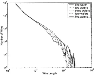
C,) 3 10 .0 = 102 z 10 10 102 10 3 105 Wire Length
Figure 1-3: Wire-length distribution of a typical circuit as a function of layers used.
number of device
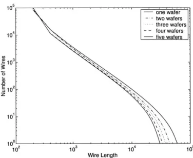
the distribution of wires in a general circuit according to their length; it finds that in a wide class of 3-D integration technologies, the wire-length distribution shifts in response to an increase in the number of device layers as shown in Figure 1-3. The leftward shift in wire-length distribution is the mechanism by which three-dimensional integration aims to improve circuit performance since the longer wires in any such distribution disproportionately affect cycle time, energy consumption, and routability.
While the general behavior exhibited in Figure 1-3 may be characteristic of 3-D in-tegration, the precise scale and separation of the distributions are what result in specific performance improvements. These particular aspects are highly dependent on the choice of technology itself. For this reason, we must first seek to understand what characterizes a potential three-dimensional integration technology.
1.2
Three-Dimensional Integration Technology
There are many technologies that can be described, however loosely, as three-dimensional. The fundamental traits underlying these technologies are that active devices may be stacked in multiple layers and that the scalability of circuit dimensions along all three axes is not inherently limited. These various technologies may be classified as either packaging tech-nologies, by which three-dimensionality is achieved after the individual 2-D chip components
10 5 - one wafe two wafe . three wa - - four wafe - five wafr r rs fers ers rs 10 4
die 3 die 2 die 1 interconnect backplane die 2
E
I
die 1 (a) (b)Figure 1-4: (a) Vertical multi-chip module (MCM-V) schematic. (b) Schematic of flip-chip bonded circuit.
have been fabricated, or monolithic technologies, by which the full 3-D structure is formed prior to packaging. In all cases, understanding how the 3-D technology parameters will affect circuit performance is the ultimate goal.
1.2.1 Packaging Methods
The first packaging technology capable of forming three-dimensional circuits is the vertical multi-chip module (MCM-V) [10, 11]. In an MCM-V package, individual dice are fabri-cated and bonded to printed-circuit-board (PCB) backplanes. The input and output pads are wire-bonded to connections on the surface of the PCB. The separate PCBs are then connected to a high-bandwidth interconnect backplane that serves as the communication
infrastructure between the dice. Figure 1-4(a) gives a schematic view of the structure of a generic MCM-V package, and Figure 1-5 shows a candidate MCM-V technology [1, 12,13]. The principal trade-off associated with this type of package is that while its manufacturing does not involve any unusually complicated processing steps, the resulting layer inter-connect is neither high-performance nor low-latency compared with wires on the individual chips.
Two approaches that attempt to overcome this performance limitation to some degree are ultra-thin chip stacking [14,15] and multilayer thin-film packaging (MCM-D) [16]. In these technologies, individual dice are prepared, stacked, and bonded using a benzocy-clobutene (BCB) polymer spin-on. The preparation stage involves whole-wafer thinning (down to 10-15 pm) before die cut; stacking is performed with an alignment accuracy of
Figure 1-5: Vertical multi-chip module (MCM-V) showing inter-layer interconnect back-plane. Left: schematic; right: package photo (reprinted from [1]).
+10 im. Once the dice are bonded, they are wired to a surrounding ring of routing tracks
for inter-layer interconnection.
These technologies offer better performance than MCM-V due to their somewhat lower-latency inter-layer interconnect. At the same time, they simultaneously offer a degree of design simplicity since the inter-layer interconnect is at the periphery. However, as with
MCM-V, the inter-layer communication occurs through the periphery. This interconnect
thus exhibits lower performance compared to within-die wires.
An alternative approach that potentially can be used to create 3-D ICs with higher-performance inter-layer interconnect is known as flip-chip bonding or chip-scale packaging
[17]. Typically used for direct mounting of circuit substrates onto PCBs, the flip-chip method is nonetheless capable of being used as a 3-D integration technology. In flip-chip bonding, the upper surface of a die is patterned with a solder-bump interconnect. The mating surface on the PCB is patterned with pads. The die is then "flipped" onto the PCB and bonded using the solder bumps. Figure 1-4(b) shows a schematic, and Figure 1-6 shows
a sample solder-bump array.
Since no fundamental constraint exists requiring the use of a PCB as the mating surface, the flip-chip approach can be used to bond two dice together. Furthermore, a platform has been suggested by which several small, customized, high-performance dice are flip-chip bonded to a larger moderate-performance die in order to integrate various high performance technologies without significant fabrication cost or compromised performance. Of course, this technique is not immediately scalable to stacks more than two dice thick; some form of through-die interconnect must be developed for such cases. Furthermore, while the solder-bump interconnect performance exceeds that of bond wires (and thus the MCM-V interconnect backplane), it still lags behind the performance of on-chip interconnect.
Transferred "O~ microsolder
(a) bumps
(b)
Figure 1-6: Flip-chip package with solder-bump interconnect (reprinted from [2]).
1.2.2 Monolithic Approaches
The goal of monolithic 3-D integration is to overcome the scalability and performance
limitations of the aforementioned packaging methods. Thus, all such integration approaches attempt to use wafer-level fabrication techniques to build device and interconnect layers directly on top of the existing conventional plane of transistors.
The first two such techniques are epitaxy and solid-phase recrystallization. In an epi-taxial 3-D integration process, silicon seed openings are fabricated alongside transistors in a conventional single-plane process. These seeds are then used to grow transistors on top of the existing devices and metallization [18]. While significant density improvements have been shown by fabricating actual circuits using this technique, it is not clear how to scale the process to more than two active layers. In a solid-phase recrystallization process, amorphous silicon is deposited on an existing integrated circuit; this silicon is then recrystallized using a laser. The resulting silicon islands may be used to produce polysilicon thin-film transistors. Thus, while this technique is highly scalable, it does not yield high-performance devices on the upper device layers, and its use is restricted to high-density memories [19,20].
The remainder of the monolithic approaches may be classified under the term "wafer bonding." The individual wafers in such a 3-D IC are fabricated using conventional means and fused together with an inter-wafer electrical and mechanical interconnect. Wafer-bonding methods differ in terms of the Wafer-bonding material and the order of fabrication
oper-*
MM MM MM
.. inter-layer interconnectdevice layer 2 layer-to-layer bond
device layer 1
Figure 1-7: Wafer-bonded structure with two device layers and copper interconnect inter-face. (Figure courtesy A. Fan, MIT.)
ations. The bonding interface may be either metal or dielectric; the individual wafers may be fabricated in parallel or sequentially.
The MIT method, for example, is a copper-bonded parallel approach [21]. Front-end and back-end processing are done separately on the individual wafers that make up a given 3-D
IC. The bottom-most wafer is typically a bulk silicon wafer, 500-700 Lrm thick, in order to
provide structural rigidity; subsequent wafers are silicon-on-insulator (SOI), 1-2 im thick, to provide scalability and high-performance interconnect. A diagram of a copper-bonded
two-wafer structure is shown in Figure 1-7.
In contrast, the MIT Lincoln Laboratory method uses oxide bonding in its parallel approach [7]. The individual wafers are processed (front end and almost all back end) before bonding. Formation of inter-wafer interconnects is the remaining back-end step. This occurs after bonding since the use of oxide as a bonding material prevents the formation of ohmic contacts as a result of the bond (although capacitive, i.e. AC-coupled, inter-wafer communication has been proposed, as in [22]). Inter-wafer interconnects are formed as vias that are etched through the the entire metallization stack of the top wafer. Thus, a greater routing-area penalty is incurred; additionally, there are more stringent alignment requirements due to the nature of the via formation. Figure 1-8 shows a multiple-wafer structure using this bonding methodology.
Researchers at Rensselaer Polytechnic Institute have developed a similar process [23]. In this method, a dielectric polymer glue, e.g. BCB, is used in place of oxide bonding. The remaining process steps are essentially the same.
Figure 1-8: Multiple-wafer structure using oxide as the bonding interface. The inter-wafer interconnects are formed after bonding. (Figure courtesy MIT Lincoln Laboratory.)
Now 10. =11 w mo d
I-
J--1. Cu patterning on SOI 2. Bond to handle wafer 3. Thin back SOI wafer,
device wafer stop on buried oxide
Oman*****mimu
4. Etch vias 5. Via filling 6. Cu patterning
Figure 1-9: Handle-wafer attachment, grindback, via formation, and copper patterning steps of the wafer bonding process. (Figure courtesy A. Fan.)
given wafer has been processed, a blank wafer is bonded to it. The inter-wafer interconnects are fabricated together with first-level metal. Since the bonding wafer is blank, there are no alignment concerns during bonding, which results in potentially smaller inter-wafer interconnects when compared with any of the previous process technologies. However, the trade-off is that the finished bottom wafer must now endure the processing steps required to fabricate devices and wires on the blank wafer that has already been bonded to it.
1.2.3 Sample Process Flow: Copper Wafer Bonding
In order to understand the design trade-offs that arise from 3-D integration technology, it is useful to examine a sample process flow. We outline here the copper wafer bonding process
of A. Fan et al. [21].
Figure 1-9 shows the pre-bonding process steps. This process starts with an existing wafer or stack of already-bonded wafers. To this stack we wish to bond another wafer, for which we use a typical SOI substrate (100 nm silicon with 400 nm buried oxide). This
sub-*T 35 aa a3 a) Alignment 1 m
7. Bond to another b) Bond at 400'C 8. Release handle water device wafer
Figure 1-10: Thermocompression and handle release steps of the wafer bonding process. (Figure courtesy A. Fan.)
strate is essentially a finished circuit, as it contains all the desired devices and interconnect. If this wafer is to be bonded again (i.e. to a third wafer), it is first metallized to produce its half of the required inter-wafer connections (step 1). The wafer is then attached to a handle that is used for mechanical manipulation (step 2). The bulk silicon is then removed from the wafer (step 3); this involves a combination of mechanical grindback and chemical etching. Inter-wafer connections to the existing stack are then formed (steps 4-6). Via formation in these steps is a conventional process technique; thus, the resulting vias can be as narrow as 0.25-0.5 .±m with an aspect ratio of 2:1.
In Figure 1-10, we show the bonding and handle-wafer release steps. The bonding process itself (steps 7a and 7b) is done at 350*C and 4000 mbar for 30 minutes. After bonding, the stack is annealed in nitrogen ambient for an additional 30-60 minutes. Wafer alignment is the critical process step. Both wafer-to-wafer alignment and bonding are performed in an Electronic Vision EV 450 Aligner and AB1-PV Bonder. The system has an inherent t3 Lm alignment tolerance, resulting in a copper-bonding pad pitch of at least
6 Rm. Thus, wafer-to-wafer alignment is the ultimate factor in determining the inter-layer
via density. With better optical alignment systems, it is possible to decrease the copper pad size down to approximately 0.5 to 1 ptm, which corresponds to a substantial increase in via density. For the remainder of this dissertation, we will assume that this via density can be achieved.
The process flow iteration is completed by releasing the handle wafer (step 8). The resulting stack is ready for either packaging or subsequent bonding of additional wafers.
1.3
Design Tradeoffs Associated with the 3-D Integration
Process Flow
Having illustrated the process flow, let us now consider the circuit-design trade-offs that arise. The copper-wafer bonding process previously outlined introduces distinct opportuni-ties and challenges for both digital and mixed-signal 3-D integration.
1.3.1 Digital ICs
In a multi-layer digital system, the system components must be partitioned among the
various layers. Thus, performance of the inter-layer interconnect is the process characteristic of primary interest.
In some of the packaging approaches described above, such as MCM-V or ultra-thin chip stacking, inter-layer wires must be routed to the periphery of individual layers before the wires may cross from layer to layer. As a result, the bandwidth and density of these wires are limited.
In contrast, some packaging technologies and all monolithic approaches offer a higher-density interconnect that may be fabricated at the local level. The trade-off between these technologies lies in the specific parasitic values associated with the interconnect; these may range over several orders of magnitude from copper-bonded approaches to solder-bump-interconnect technologies.
In addition, the choice of integration technology may affect signal-coupling issues. The adjacency of two substrates to a given set of metal layers reduces the amount of charge sharing between adjacent metal lines [25]. The extent to which this coupling is reduced depends on the effective capacitance between the given metal lines and the second sub-strate (introduced by 3-D integration). Higher subsub-strate capacitance reduces inter-symbol interference at the expense of increasing overall capacitive energy dissipation.
1.3.2 Analog/Mixed-Signal ICs
Three-dimensional integration also provides benefits and challenges for mixed-signal and mixed-technology circuits. In analog circuits, the inter-wafer interface may be used to isolate functional units [25]. Depending on the choice of technology, or even the use of metal vs. dielectric in a specific wafer-bonding technology, the degree of isolation may be
affected significantly.
3-D integration also allows for the incorporation of multiple fabrication technologies
within a single circuit or package. For example, silicon CMOS may be integrated with SiGe or InP analog, or logic-optimized CMOS may be integrated with CMOS optimized for SRAM, DRAM, or high-voltage non-volatile memories. This type of integration presents unique opportunities for circuit design; however, the integration of a small number of rel-atively large, discrete macro blocks in a single circuit also presents some unique design partitioning and optimization issues.
1.4
Overview of Previous Work
1.4.1 Stochastic Modeling of 3-D ICs
The bulk of prior work on 3-D integrated circuits has been in system-level stochastic mod-eling. Numerical models have been derived that estimate the wire-length distribution in circuits implemented in various forms of 3-D integration technology [8,26-29]. The bulk of this form of analysis has resulted in plots of the form shown in Figure 1-3.
Extensions to these models have considered specific 3-D IC technology optimizations such as variable inter-wafer distance [30]. Other ventures in the area of numerical modeling concern specific performance issues such as heat generation [31, 32]. The remaining work along these lines has been in numerical modeling of specific circuit architectures in 3-D.
1.4.2 Architectural Investigation
In addition to numerical analysis of general-purpose circuits targeted for 3-D integration, several specific circuit architectures have been ported to candidate 3-D IC technologies. The prime candidates for 3-D integration explored thus far have been imagers and sensors, microprocessors, and field-programmable gate arrays (FPGAs).
Imager circuits consist of a two-dimensional array of optical sensors together with cir-cuitry to process and deliver the sensed images off-chip. In circuits such as [33], benefit from 3-D integration is due to the fact that in conventional implementations, there is a per-pixel overhead for the processing and delivery circuitry. In a 3-D implementation, the additional wafers can be dedicated for the non-sensing components. As a result, a greater pixel density can be achieved.
A similar density impact is to be gained in FPGAs [9,34]. Like imagers, FPGAs consist
of a regular array of elements. In this case, the elements are programmable functional units (typically a logic function with four to six inputs and one or two outputs, together with optional registers or tri-state drivers) and the overhead consists of wires and programmable switchboxes used to interconnect the functional units. However, with FPGAs the intercon-nect may consume as much as 90% of the total circuit area. The benefit of 3-D integration is that the extra routing resources in the third dimension can be used to reduce the number of conventional routing tracks required, thus increasing the density of functional units as well as shortening the wires used to connect them.
In microprocessors, a number of architectural improvements have been proposed to exploit 3-D integration [35,36]. In general, the microprocessor has been analyzed as a logic-memory system; performance enhancement is achieved either by (1) partitioning both logic and memory subsystems to reduce the logic latency as well as the memory latency, or (2) increasing the memory capacity of the system. In [35] it was determined that microprocessor instructions-per-cycle (IPC) could be increased by 20% to 30% using two-wafer integration. Furthermore, at current technology nodes, long-wire delay in microprocessors could be reduced by a factor of 2.5 to 5. Finally, it was predicted that in future technology nodes, opportunities for increased memory subsystem performance due to 3-D integration would significantly increase performance as measured by IPC.
1.4.3 Unresolved Problems
The above avenues of prior research still leave open a number of problems. First, in the area of stochastic modeling, is the question of validity: without any analysis of placed and routed circuits, it is impossible to verify that the models' predictions are correct. In fact, the models themselves vary greatly in terms of their analyses of 3-D IC performance - due in part to varied technology assumptions and to intrinsic issues of model accuracy. Of more direct importance along this line of investigation is actual circuit performance. Without having vetted predictive models for 3-D circuit wire length, it is very difficult to make
reasonable predictions for circuit timing and energy consumption in three dimensions. Second, in the area of architectural investigation, the opposite problem arises. In this area, specific opportunities for 3-D integration have been identified. However, it is not known to what extent the improvements in these circuits can be leveraged in general.
Third, in either of the above cases, it is desirable to make further circuit-based analyses of 3-D ICs. Issues such as thermal performance and technology scaling have yet to be addressed completely.
It is clear that what is needed is the ability to analyze actual circuits in a variety of
3-D implementations. Furthermore, this analysis must be carried out in a general-purpose
manner, independent of architecture.
1.5
Contributions of this Dissertation
This dissertation makes two overall contributions to the understanding of 3-D integration. The first is a computer-aided design flow for 3-D ICs; the second is the performance analysis of digital 3-D ICs and IC components.
We present our design flow and algorithmic details of the tools in this flow in Chapter 2. Our analysis of circuit performance begins with an adaptation of the stochastic models mentioned in Section 1.4.1 for a set of benchmark circuits used throughout the dissertation. We analyze the wire-length performance of these circuits through the use of the models and compare this data with measurements from placements generated by our tools (Chapter 3). We proceed to expand upon the predictions of the models by utilizing specific placement-based analyses. Having established the wire-length behavior of 3-D ICs, we develop a placement-based characterization of circuit timing and energy performance (Chapter 4).
We bring our design tools to bear on a significant problem in 3-D ICs: heat genera-tion and removal (Chapter 5). With the use of placement-based analyses, we verify prior numerical simulations of thermal effects in 3-D ICs. Furthermore, we characterize ther-mal behavior in two placement contexts by demonstrating how placement-based therther-mal optimization can be utilized to obtain more acceptable behavior in exchange for reduced performance in other metrics. We also consider in detail the use of advanced heat-removal technologies and develop design models and guides for the implementation of such tech-nologies within a 3-D system.
We also examine some speculative issues regarding the future of 3-D IC design
(Chap-ter 6). First, we consider how the performance improvements due to 3-D integration might
scale in conjunction with conventional technology scaling. Second, we explore how to ex-pand the design flow to include mixed-signal integration. In the context of mixed-signal
integration, we examine how digital performance may be improved, and we also evaluate some methods for reducing the noise impact of these digital circuits in mixed-signal 3-D ICs. Finally, we propose a design-flow architecture for mixed-signal 3-D integrated circuits.
Chapter 2
Design Tools for
Three-Dimensional Integrated
Circuits
2.1
Overview
The design of a digital integrated circuit typically proceeds from a high-level specification of what the circuit is supposed to do by successively refining this specification down to the
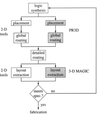
function of each individual transistor. Refining from specification to transistor layout may be done all at once; however, for all but the smallest circuits, this is intractable for both humans and computers. Thus, the design process is divided into steps such as those shown in the left half of Figure 2-1. Our goal is to identify which components of this design flow must be replaced or altered to design three-dimensional integrated circuits.
As seen in Figure 2-1, several steps are taken to produce fabrication data from a high-level specification. We take this specification to mean a behavioral or functional description in a hardware description language such as VHDL or Verilog. Thus, the first step is typ-ically logic synthesis, whereby a gate-level circuit net list is determined. A floorplan is developed, and given the net list and physical parameters of the individual logic gates, the circuit gates are placed in an optimal location on the die. The resulting placement is wired or routed. The placed-and-routed circuit layout is analyzed to ensure that if fabricated according to the design, it will function according to the specification. These
logic
synthesis
placement placemient
2-D PR3D
tools global global routing routing
detailed routing
2-D layout layout 3-D MAGIC
tools extractionacion toeets nW spec.? yes fabrication
Figure 2-1: Simplified flowchart for the automated design of 2-D and 3-D digital integrated circuits.
three components - synthesis, placement, and routing - constitute the front end of physical design of digital circuits.1
As indicated in the right half of Figure 2-1, at several stages of the flow it is required or desired to modify the tools to design for three-dimensional integration. In the next several sections, we will address when conventional tools may be used, what changes may be required for such tools, and what tools we have developed to enable 3-D IC design.
2.2
Logic Synthesis
Logic synthesis remains for the most part a technology-independent phase of the design flow. The output of logic synthesis is a gate-level description of a circuit; the functionality provided by the gates themselves is independent of how these gates are fabricated. Thus, it is not strictly necessary to modify this stage of the design flow to create 3-D ICs.
However, some optimizations exist that take advantage of technology-dependent infor-mation. For example, gate vendors may offer various speed and power options for individual gates [37]. Additionally, these gates perform differently under varying input and output
con-'For the purposes of proper scoping, the back end of design, including components such as reliability, yield, and other such post-layout analyses, will not be addressed in this thesis.