HAL Id: hal-01590613
https://hal.archives-ouvertes.fr/hal-01590613
Submitted on 19 Sep 2017HAL is a multi-disciplinary open access
archive for the deposit and dissemination of sci-entific research documents, whether they are pub-lished or not. The documents may come from teaching and research institutions in France or abroad, or from public or private research centers.
L’archive ouverte pluridisciplinaire HAL, est destinée au dépôt et à la diffusion de documents scientifiques de niveau recherche, publiés ou non, émanant des établissements d’enseignement et de recherche français ou étrangers, des laboratoires publics ou privés.
Integrated temperature sensor with diamond Schottky
diodes using a thermosensitive parameter
Gaëtan Perez, Gauthier Chicot, Yvan Avenas, Pierre Lefranc, Pierre-Olivier
Jeannin, David Eon, Nicolas Rouger
To cite this version:
Gaëtan Perez, Gauthier Chicot, Yvan Avenas, Pierre Lefranc, Pierre-Olivier Jeannin, et al.. Integrated temperature sensor with diamond Schottky diodes using a thermosensitive parameter. Diamond and Related Materials, Elsevier, 2017, 78, pp.83-87. �10.1016/j.diamond.2017.08.008�. �hal-01590613�
Integrated temperature sensor with diamond Schottky diodes using
a thermosensitive parameter.
Gaëtan Perez1, Gauthier Chicot2, Yvan AVENAS1, Pierre LEFRANC1, Pierre-Olivier JEANNIN1, David EON2, Nicolas ROUGER3
1
Université Grenoble Alpes, CNRS, G2Elab, F-38000 Grenoble, France
2
Université Grenoble Alpes, CNRS, Institut Néel, F-38042 Grenoble, France
3
Université de Toulouse ; LAPLACE ; CNRS ; INPT ; UPS, F-31071 Toulouse, France
Abstract - Diamond Schottky diodes with high figures of merit have been previously demonstrated. However, self-heating during characterization process has been widely observed and fast and high temperature monitoring is highly desired, moreover temperature management is of high interest for device parallelization. In this article, we investigate the possibility to monolithically integrate a small area Schottky diode which will be used as temperature sensor. The diode voltage drop at a constant forward bias current will be used as a thermosensitive parameter. This voltage drop has a quasi-linear variation over a temperature range (experimentally demonstrated from 300 K to 440 K in this study due to the maximum operating temperature of the experiments) at constant bias current densities between 0.25 A/cm² and 2.5 A/cm², with a sensor sensitivity of -1.6 mV/K. It is also demonstrated that this integrated temperature sensor is affected by the biasing conditions of the main Schottky diode. To perform reliable measurements, the temperature measurement must be done while the main Schottky diode is in OFF-state or the fabrication process must be modified. This integrated temperature measurement allows accurate junction temperature monitoring, offering a diamond Schottky diode operation at its best ON-state performance through an active device temperature management.
I. INTRODUCTION
Diamond is considered as the ultimate material for semiconductors for power electronics applications, with higher figures of merit than the other wide-bandgap semiconductors [1]. Schottky diodes have been realized worldwide and show promising performance results with high breakdown voltage capability [2], [3], low loss and high temperature operation [4]–[8]. Boron doped CVD diamond is widely used for these Schottky diodes, offering the best performance in specific ON resistance (RonS) vs. Breakdown Voltage. The incomplete ionization of Boron dopants at room
temperature allows diamond semiconductors to have a lower Ron at higher temperature [4], [7].
Then, the self-heating effect of diamond power electronic devices can be used to improve the forward performance of the semiconductor by decreasing forward losses [6], due to the improved ionization of Boron dopants and a negligible decrease of the carrier mobility. A particular care is required for diamond Schottky diodes as they exhibit a negative (from 0 K to 400-600 K) and positive (above 400-600 K, doping dependent) temperature coefficient [9], [10]. The measured ON-state resistance of a 500 µm x 500 µm diamond diode presented in Figure 1 shows an optimized operation of the diamond device at 450 K. Active temperature management is then necessary for diamond semiconductor by optimizing the ON-state semiconductor losses. Accurate temperature information is highly required for such a temperature management. Moreover, as the size of the diamond substrate is still limited, it is needed to consider the parallelization of semiconductors or switching cells in order to increase the effective current of a power converter based on diamond devices. However, paralleled devices requires extra attention on its current balancing [11]. For a switching cell parallelization, even if the devices are assembled on a common thermal substrate, the temperature of the devices can be different, inducing unbalanced current between each paralleled leg. Detecting a large temperature difference between the devices and modifying the hottest switching cell will avoid the current to be unbalanced. Such an active parallelization will be allowed by accurate temperature measurement at the device level, offering the possibility to react and control the current flow to hottest or coolest leg.
Figure 1 : Measured 500 µm x 500 µm diamond diode ON-state resistance as a function of the device temperature. A 200nm p+ Layer is grown on a Ib HPHT diamond substrate, a 1.3 µm p- Layer doped at 5.1015 cm-3 is then grown on the p+ Layer.
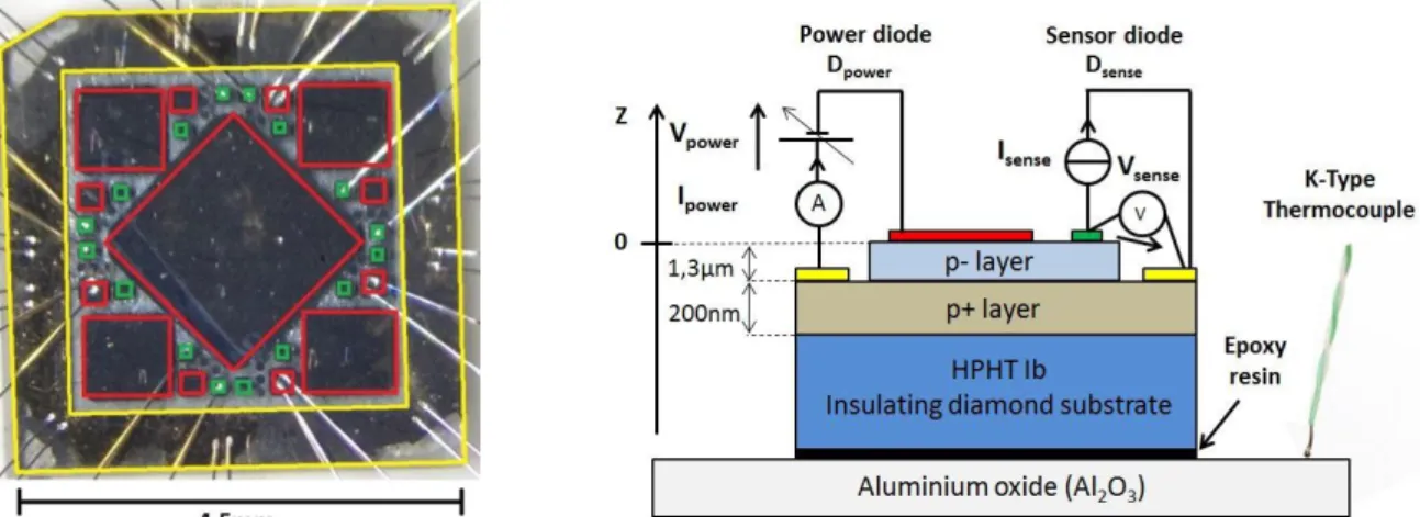
We propose here a solution to accurately estimate the junction temperature using a thermosensitive electrical parameter of a monolithically integrated diamond diode. The fabrication process has already been described [5]. The monolithically integrated Schottky diodes have a common anode (Ohmic contact: Ti(20 nm) / Pt(20 nm) / Au(10 nm)) and isolated cathodes (Schottky contacts : Zr(30 nm) / Pt(20 nm) / Au(10 nm)) although no specific Junction Termination Extension (JTE) is included. Figure 2 presents the fabricated sample with the used electrical parameters, containing several large area power diodes (highlighted in red) and small area temperature sensor diodes (highlighted in green). 3D simulations have shown that static and transient temperatures are very close between the power diode and the sensor diode.
Figure 2 : Picture and schematic cross-section of the diamond diode sample with the Power diodes in red, the sensor diodes in green and the common ohmic contact in yellow
II. MATERIAL AND METHODS
Multiple studies have been already conducted to use thermosensitive electrical parameters (TSEP) of diodes in the case of Silicon (Si) and Silicon-Carbide (SiC) devices [12]–[14]. The diode voltage drop at a low forward bias current is a widely used method due to its easy calibration and the linear variation of the diode voltage drop as a function of the operating temperature [15]. The low bias current density insures a sensor diode operation in the exponential regime of its characteristic, where the ON-state resistance has a negligible impact. Then, the thermosensitive electrical parameter has a negative temperature coefficient in the whole temperature range and is not impacted by the negative and positive temperature coefficient of the ON-state resistance (Figure 1). In our study, the thermosensitive parameter of a 200 µm x 200 µm diamond diode is first calibrated from room temperature (RT, 300 K) to 440 K at several bias current densities. The temperature of a power diode is then measured with this thermosensitive parameter allowing us to analyze the behavior of this thermosensitive parameter with another diode in operation on the same substrate.
The diamond sample presented in Figure 2 has been glued with epoxy resin on a metallized alumina (Al2O3) substrate, with bonding wires connecting the electrical contacts. This partially
packaged sample has been calibrated in a temperature regulated oven with K-type thermocouple placed on the alumina substrate to have reliable device temperature information, as a uniform temperature inside the oven is considered. The oven temperature has been set from RT to 440 K, the highest temperature has been limited by the maximum operating temperature of the measurement connectors and wires inside the oven. An Agilent B1505A Power Device Analyzer / Curve Tracer is used to extract the Current (Isense), Voltage (Vsense) characteristics of the diode at different
temperatures. These characteristics are shown in Figure 3. A pulsed source has been used to bias the diamond diode acting as a temperature sensor. The pulsed current source is used to limit the self-heating effect on the sensor diode during the calibration process. A pulse time of 1 ms with an OFF time of 50 ms between two pulses has been used. The device is cooled down during the OFF time between two pulses, decreasing the device self-heating phenomenon and allowing us considering the temperature of the device as the one of the oven temperature.
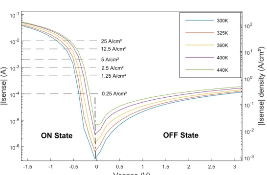
Figure 3 : Current-Voltage characteristic of the calibrated 200 µm x 200 µm diode, the diode is anode grounded. The substrate temperature has been externally set by a temperature regulated oven, and measured by K-type thermocouple.
The variation of the diode voltage drop (Vsense) as a function of the operating temperature
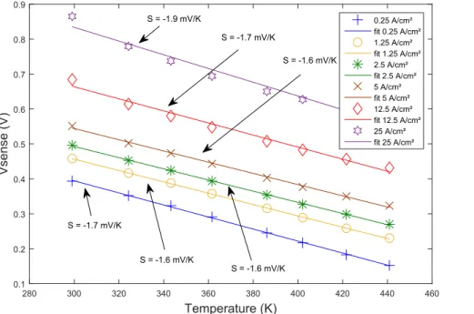
has been extracted from the Current, Voltage characteristics. In the diode exponential regime (low ON State current), the diode voltage drop variation over the temperature is extracted for a given current density, as shown by the horizontal dash lines in the Figure 3. Results of the temperature sensitive electrical parameter extraction are presented in the Figure 4 for bias current densities from 0.25 A/cm² to 25 A/cm², corresponding to diode power densities from 0.1 W/cm² to 22.5 W/cm². Vsense has a linear variation over the temperature range for current densities up to 5 A/cm², with a
R²>0.994 (R² is the sensor sensitivity linear extrapolation coefficient of determination) and a temperature sensitivity from -1.6 mV/K to -1.7 mV/K. These low bias current densities allow us to have a negligible device self-heating effect with a maximum power density of 5.4 mW/cm² at the scale of the 4.5 mm x 4.5 mm substrate. The linearity of the sensor sensitivity has not been experimentally demonstrated for higher temperature due to the limitation of the experiment temperature. However, to extend a linear sensitivity at high temperature, the sensor bias current can be increased. A 2.5 A/cm² sensor diode current density is used at low temperatures while 5 A/cm² can be used for high temperature measurement. These sensitivities are lower, but in a same order of magnitude, than those found with 4H-Silicon Carbide diodes [13]. The higher current densities do not allow for a linear variation of the thermosensitive parameter over the whole temperature range, since higher current densities are governed by a combination of series resistance and the
modification of the Schottky barrier height. These bias current densities cannot be used for a linear temperature measurement. Such linear variation of the temperature sensitive electrical parameter can also be obtained for Schottky contacts made of other metals. However as the Schottky barrier height ans the ideality factor will be modified, the voltage level and sensor sensitivity for a given bias current density will be changed. The TSEP has to be calibrated for this Schottky contact metals.
Figure 4 : Diode voltage drop as a function of the operating temperature for given bias currents, the diode Thermosensitive Electrical Parameter has been extracted.
III. RESULTS
The self-heating of a diamond power diode (Dpower) during ON-state characterization is now
used to analyze the temperature information given by the thermosensitive parameter from another diamond diode integrated on the same sample. The self-heating phenomenon increases the device temperature due to the high power dissipated in the power diode. This temperature is measured by the sensor diode (Dsense) thermosensitive parameter for an external temperature set at 295 K. Dsense is
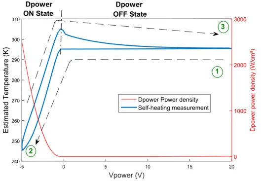
biased at a 2.5 A/cm² forward current density to have a temperature sensor sensitivity of -1.6 mV/K. The power diode is biased (Vpower) with a staircase profile of 300 mV steps, the step time is set to 1
second to have a significant self-heating phenomenon. The evolution of the measured temperature as a function of Dpower bias is presented in Figure 5. The power diode is biased from 20 V reverse to 5
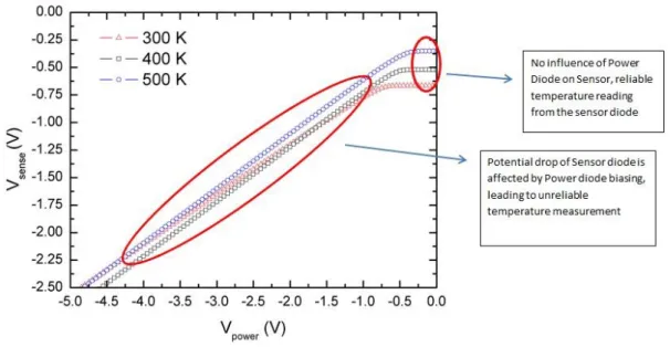
V forward (1 to 2 in the Figure 5) and back to 20 V reverse (2 to 3) while the sensor diode is biased at a constant current density. The high power density dissipated in the power diode increases the
device temperature involving a hysteretic profile, the device temperature is then slowly decreased when the power diode is OFF due to the device thermal inertia. An influence of the Dpower conduction
on Dsense is clearly observed in Figure 5, considering that the estimated temperature seems to
decrease when the power diode is ON which is not true. Due to an overlap of the current path of the two diamond diodes within the same p-/p+ layers, Dsense is affected by the forward current of Dpower,
involving errors on the temperature measurement. A temperature measurement using this method involves measurement error (∆ Terror) as high as 50 K, if the temperature is extracted from Dsense while
Dpower is in ON-state at high forward current densities.
Figure 5 : Temperature measurement by using the thermosensitive parameter as a function of Dpower
(common anode grounded) polarization at an operating temperature of 295 K.
3D numerical simulations have been performed in the view of quantitatively investigating this phenomenon. Atlas3D from Silvaco has been used for 3D Finite Element analyses, where the diamond material properties have been set accordingly to [16], [17]. A smaller surface of 500 µm x 500 µm has been simulated (Figure 6) mainly to limit the computing requirements while describing the same interactions between two monolithically integrated diamond Schottky diodes. The simulated p- layer has been set to 1 µm with the same doping as the fabricated sample, and a 1 µm-thick p+ substrate has been simulated to act similarly as the common anode metallization. Schottky barrier heights were set to 1 eV (6.1 eV work function). Figure 7 clearly reproduces the trend observed in the experiments, where the current density of the power diode modifies the ON-state voltage drop of the sensor diode.
Dpower Dpower
Figure 6 : Extracted potential distribution in the XY-plane at z=-0.99 µm of the simulated diamond devices (1 nm above the p+/p- junction): two Schottky contacts are integrated on the same sample, with common anode contacts. The power diode is biased in ON-state at 1000 A/cm² and the sense diode is biased in ON-state at 3.9 A/cm².
Figure 7 : Simulated DC sense diode cathode potential as a function of the power diode cathode potential and ambient temperature. The sense diode has been biased at 3.9 A/cm² in forward regime.
IV. DISCUSSIONS
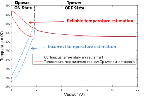
To solve this issue of inaccurate and bias dependent temperature measurement, two solutions are possible. First, the temperature measurements can be done when Dpower is in OFF-state
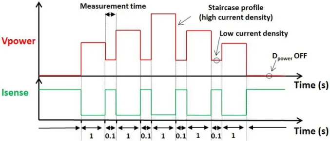
to have accurate device temperature information. Such a measurement is presented in the Figure 8 for an external temperature set at 295 K. The power diode bias profile previously discussed has been
modified by adding a 100 ms measurement time between each step as shown in Figure 9. The power diode is biased at a low power density during this measurement time to accurately measure the device temperature with the thermosensitive parameter. As the temperature measurement is done at a low power diode current density, the sensor diode is no longer affected by the power diode. However, this method underestimates the device temperature since the device is cooled during the measurement time, a small measurement time is then needed to have accurate temperature information. The second option to remove the bias dependence of the thermosensitive parameter is to modify the mask layout. Such a modification targets to decouple the current tubes from the power diode and the temperature sensor. Thanks to the specifications of the diamond substrate (electrically isolating and thermally conducting), a modification of the device layout is presented in Figure 10, where an etching step is added to the previous process. It will electrically isolate the p+ anode regions of the sensor and power diodes, avoiding the power current to depolarize Dsense. The sensor diode
can be placed at the center of the diamond sample to be close to each power diode, or can be distributed to map the temperature distribution inside the sample.
Figure 8 : Temperature measurement by using the Thermosensitive Electrical Parameter when the Power diode is biased at a low current density compared to a continuous temperature measurement.
Reliable temperature estimation
Figure 9 : Schematic of the temperature measurement. Device temperature measurement by using Dsense TSEP is done at low Dpower current density.
Figure 10 also presents 3D simulations where such a deep trench has been used, in order to isolate both p+ regions and anode contacts. Thanks to the deep trenches, the integrated sensor diode is no longer affected by the power diode biasing condition and can lead to bias independent temperature measurement. The Vsense voltage difference between the results with and without
trench is due to the increase of the sensor current spreading resistance with the reduced spreading volume. The accuracy of the thermosensitive parameter will not be affected, since the thermosensitive parameter needs to be calibrated for the modified device.
Figure 10 : 3D simulation of two Schottky diodes with isolated cathodes and anodes. Right, ON-state cathode voltage drop of the sensor diode as a function of the ON-state cathode voltage for the power diode, with or without p+ isolation trench.
V. CONCLUSION
In summary, the diode voltage drop of a diode at a constant bias current has been used as a thermosensitive parameter to perform temperature measurements on a monolithic integration of diamond Schottky diodes. The diode voltage drop for a bias current of 2.5 A/cm² has a linear variation on a temperature range from 300 K to 440 K with a sensitivity of -1.6 mV/K. Due to an overlap of the current path of the integrated diodes, the diode used as a thermosensitive parameter is affected by the power diode conduction, involving temperature measurement error. 3D simulations have been performed to reproduce the effects observed in the experiments, while proposing a method to suppress the dependence on the power diode biasing conditions. Such a temperature sensor can be used for a device temperature management in the way to optimize the ON-state semiconductor losses.
ACKNOWLEDGMENT
The research leading to these results has been performed within the GreenDiamond project (http://www.greendiamond-project.eu/) and received funding from the European Community's Horizon 2020 Program (H2020/2014-2020) under grant agreement n° 640947.
The diamond samples presented here as examples, have been fabricated by CNRS/NEEL in the framework of A. Traore PhD thesis, T.T. Pham PhD thesis, Univ. Grenoble Alpes AGIR program, ANR DiamMem and DGE DIAMONIX2.
This research is partially funded by French ANR Research Agency under grant ANR-16-CE05-0023 #Diamond-HVDC
REFERENCES
[1] B. Ozpineci and L. M. Tolbert, Comparison of Wide-Bandgap Semiconductors for Power Electronics Applications. 2003.
[2] P. N. Volpe, P. Muret, J. Pernot, F. Omǹs, T. Teraji, Y. Koide, F. Jomard, D. Planson, P. Brosselard, N. Dheilly, B. Vergne, and S. Scharnholz, “Extreme dielectric strength in boron doped homoepitaxial diamond,” Appl. Phys. Lett., vol. 97, no. 22, pp. 10–13, 2010.
[3] W. Huang, T. P. Chow, J. Yang, and J. E. Butler, “High-Voltage Diamond Schottky Rectifiers,” Int. J. High Speed Electron. Syst., vol. 14, no. 3, pp. 872–878, 2004.
[4] H. Umezawa, Y. Kato, and S.-I. Shikata, “1Ω On-Resistance Diamond Vertical-Schottky Barrier Diode Operated at 250 C,” Appl. Phys. Express, vol. 6, no. 1, 2013.
[5] A. Traoré, P. Muret, A. Fiori, D. Eon, E. Gheeraert, and J. Pernot, “Zr/oxidized diamond interface for high power Schottky diodes,” Appl. Phys. Lett., vol. 104, no. 5, p. 052105, 2014. [6] S. Tarelkin, V. Bormashov, S. Buga, A. Volkov, D. Teteruk, N. Kornilov, M. Kuznetsov, S.
Terentiev, A. Golovanov, and V. Blank, “Power diamond vertical Schottky barrier diode with 10 A forward current,” Phys. Status Solidi, vol. 212, no. 11, pp. 2621–2627, 2015.
[7] V. D. Blank, V. S. Bormashov, S. A. Tarelkin, S. G. Buga, M. S. Kuznetsov, D. V Teteruk, N. V Kornilov, S. A. Terentiev, and A. P. Volkov, “Power high-voltage and fast response Schottky barrier diamond diodes,” Diam. Relat. Mater., vol. 57, pp. 32–36, 2015.
[8] H. Umezawa, M. Nagase, Y. Kato, and S. I. Shikata, “High temperature application of diamond power device,” Diam. Relat. Mater., vol. 24, pp. 201–205, 2012.
[9] J. Pernot, P. N. Volpe, F. Omnès, P. Muret, V. Mortet, K. Haenen, and T. Teraji, “Hall hole mobility in boron-doped homoepitaxial diamond,” Phys. Rev. B - Condens. Matter Mater. Phys., vol. 81, no. 20, pp. 1–7, 2010.
[10] V. S. Bormashov, S. a. Terentiev, S. G. Buga, S. a. Tarelkin, a. P. Volkov, D. V. Teteruk, N. V. Kornilov, M. S. Kuznetsov, and V. D. Blank, “Thin large area vertical Schottky barrier diamond diodes with low on-resistance made by ion-beam assisted lift-off technique,” Diam. Relat. Mater., vol. 75, pp. 78–84, 2017.
[11] S. G. Kokosis, I. E. Andreadis, G. E. Kampitsis, P. Pachos, and S. Manias, “Forced current balancing of parallel-connected SiC JFETs during forward and reverse conduction mode,” IEEE Trans. Power Electron., vol. 32, no. 2, pp. 1400–1410, 2017.
[12] H. Luo, W. Li, and X. He, “Online high-power P-i-N diode chip temperature extraction and prediction method with maximum recovery current di/dt,” IEEE Trans. Power Electron., vol. 30, no. 5, pp. 2395–2404, 2015.
[13] N. Zhang, C.-M. Lin, D. G. Senesky, and A. P. Pisano, “Temperature sensor based on 4H-silicon carbide pn diode operational from 20 °C to 600 °C,” Appl. Phys. Lett., vol. 104, no. 7, p. 073504, 2014.
[14] S. Rao, L. Di Benedetto, G. Pangallo, A. Rubino, S. Bellone, and F. G. Della Corte, “85 K to 440 K Temperature Sensor Based on a 4H-SiC Schottky Diode,” IEEE Sens. J., vol. 16, no. 17, pp. 1–1, 2016.
[15] Y. Avenas, L. Dupont, and Z. Khatir, “Temperature Measurement of Power Semiconductor Devices by Thermo-Sensitive Electrical Parameters—A Review,” IEEE Trans. Power Electron., vol. 27, no. 6, pp. 3081–3092, 2012.
[16] A. Maréchal, N. Rouger, J. C. Crébier, J. Pernot, S. Koizumi, T. Teraji, and E. Gheeraert, “Model implementation towards the prediction of J(V) characteristics in diamond bipolar device simulations,” Diam. Relat. Mater., vol. 43, pp. 34–42, 2014.
[17] S. J. Rashid, A. Tajani, D. J. Twitchen, L. Coulbeck, F. Udrea, T. Butler, N. L. Rupesinghe, M. Brezeanu, J. Isberg, A. Garraway, M. Dixon, R. S. Balmer, D. Chamund, P. Taylor, and G. a J. Amaratunga, “Numerical Parameterization of Diamond for Device Simulation and Analysis,” IEEE Trans. Electron Devices, vol. 55, no. 10, pp. 2744–2756, 2008.