Development of Extracellular Electrophysiology
Methods for Scalable Neural Recording
by
MASSA0I
Jacob G. Bernstein
D
S.B., Massachusetts Institute of Technology (2007)
S.M., Massachusetts Institute of Technology (2009)
LI
FHUS ES INSITUTE F TECHNOLOGY
EC
12
2016
BRARIES
Submitted to the Program in Media Arts and Sciences
School of Architecture + Planning
in partial fulfillment of the requirements for the degree of
Doctor of Philosophy in Media Arts and Sciences
at the
MASSACHUSETTS INSTITUTE OF TECHNOLOGY
ARCHIVES
September 2016
Massachusetts Institute of Technology 2016. All rights reserved.
Signature redacted
Author . . . . .
Z5x1
Program in Media Arts and Sciences
Scho
f
hitecture + Planning
Certified by
.Signature
redacted-September 1, 2U16
Dr. Edward S. Boyden, III
Associate Professor of Media Arts and Sciences
Associate Professor of Brain and Cognitive Sciences
Associate Professor of Biological Engineering
__Tc
ill S Q IAccepted by...
Signature redacted
V.%O-;! i 0~i LJ [1J1 V 1nu1
...
Dr. Patricia Maes
Professor of Media Arts and Sciences
Academic Head, Media Arts and Sciences Program
MITLibraries
77 Massachusetts Avenue Cambridge, MA 02139
http://Iibraries.mit.edu/ask
DISCLAIMER NOTICE
Due to the condition of the original material, there are unavoidable flaws in this reproduction. We have made every effort possible to
provide you with the best copy available. Thank you.
2
primpli.--Development of Extracellular Electrophysiology Methods for
Scalable Neural Recording
by Jacob G. Bernstein
Submitted to the Program in Media Arts and Sciences
School of Architecture
+
Planningon September 1, 2016, in partial fulfillment of the requirements for the degree of
Doctor of Philosophy in Media Arts and Sciences
Abstract
In order to map the dynamics of neural circuits in mammalian brains, there is a need for tools that can record activity over large volumes of tissue and correctly attribute the recorded signals to the individual neurons that generated them. High-resolution neural activity maps will be critical for the discovery of new principles of neural coding and neural computation, and to test computational models of neural circuits. Extracellular electrophysiology is a neu-ral recording method that has been developed to record from large populations of neurons, but well-known problems with signal attribution pose an existential threat to the viability of further system scaling, as analyses of network function become more sensitive to errors in attribution. A key insight is that blind-source separation algorithms such as Independent Component Analysis may ameliorate problems with signal attribution. These algorithms require recording signals at much finer spatial resolutions than existing probes have accom-plished, which places demands on recording system bandwidth. We present several advances to technologies in neural recording systems, and a complete neural recording system designed to investigate the challenges of scaling electrophysiology to whole brain recording. We have developed close-packed microelectrode arrays with the highest density of recording sites yet achieved, for which we built our own data acquisition hardware, developed with a compu-tational architecture specifically designed to scale to over several orders of magnitude. We also present results from validation experiments using colocalized patch clamp recording to obtain ground-truth activity data. This dataset provides immediate insight into the nature of electrophysiological signals and the interpretation of data collected from any electrophys-iology recording system. This data is also essential in order to optimize probe development and data analysis algorithms which will one day enable whole-brain activity mapping. Thesis Supervisor: Dr. Edward S. Boyden, III
Title: Associate Professor of Media Arts and Sciences Associate Professor of Brain and Cognitive Sciences Associate Professor of Biological Engineering
This following served on the examination committee for this dissertation:
Signature redacted
...
Dr. Nancy Kopell
Professor
Co-Director, Center for BioDynamics
Department of Mathematics
Boston University
Reader ...
Signature redacted
Dr. Joseph Paradiso
Associate Professor
Co-Director, Things That Think Consortium
MIT Media Lab
Massachusetts Institute of Technology
Reader
Contents
1 Introduction
1.1 Problem Statement . . . .
1.2 Introduction . . . . 1.3 Background .... ...
1.3.1 Spike Sorting - Clustering and ICA . . . .
1.4 Outline of Chapters . . . . 2 Hardware for Scalable Electrophysiology
2.1 Introduction . . . . 2.2 R esults . . . . 2.2.1 System Design . . . . Probes .... ... Headstages . . . . Data Acquisition . . . . 2.3 D iscussion . . . . 2.4 M ethods . . . . 2.4.1 Probes . . . . 2.4.2 Headstages . . . . 2.4.3 Data Acquisition . . . . 2.5 Contribution . . . . 3 Spike Sorting with Close-Packed Electrode Arrays
3.1 Introduction . . . . 13 13 14 16 17 18 23 23 24 25 25 27 29 32 36 36 38 38 42 45 45
3.2 Results .4
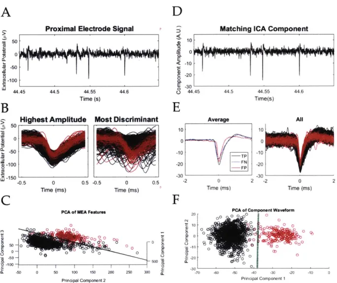
3.2.1 ICA on Ground-Truth Recordings . . . .
3.2.2 Analysis of Multi-Unit Independent Components . . . .
3.3 D iscussion . . . . 3.4 M ethods . . . .. . . . 3.4.1 Surgical Procedures . . . .
3.4.2 Colocalized Electrophysiology Recordings . . . .
3.4.3 Data Acquisition and Analysis Pipeline . . . .
3.4.4 Pipette Position Estimation . . . .
3.4.5 Spike Identification in Patch Signal and Burst Exclusion
3.4.6 Filtering and Artifact Subtraction in MEA Signal . . . .
3.4.7 ICA Implementation . . . .
3.4.8 Matching Independent Components to Patched Neuron .
3.4.9 Feature Extraction and Discriminant Analysis . . . .
3.5 Contribution . . . . . . . . 47 . . . . 50 . . . . 53 . . . . 55 . . . . 55 . . . . 56 . . . . 58 . . . . 60 . . . . 63 . . . . 65 . . . . 68 . . . . 68 . . . . 68 . . . . 70 4 Devices for 3D Neuromodulation
4.1 Introduction . . . .
4.2 R esults . . . .
4.2.1 Fiber array design, fabrication, and operation . . . . 4.2.2 Implantation, utilization, and validation of fiber arrays in behaving mice 4.2.3 Integration of electrophysiological recording and fiber array illumination 4.3 D iscussion . . . . 4.4 M ethods . . . .
4.4.1 LED and Fiber-coupled LED Array Fabrication: Design and
Prepara-tion of Key Structural Components . . . .
4.4.2 Fiber Array Fabrication: Preparation of Other Components...
4.4.3 Fiber Array Fabrication: Assembly . . . .
4.4.4 LED Driver Circuit Design and Operation . . . .
4.4.5 Fiber Array Testing: Light Power . . . . 77 77 78 78 86 86 86 89 89 89 90 92 92 8 47
4.4.6 Fiber Array Testing: Thermal Testing In Vivo . . . . 93
4.4.7 Fiber Array Fabrication: Optimization for Electrophysiology . . . . . 93
4.4.8 Electrophysiological Recording and Data Analysis . . . . 94
4.4.9 Fiber Array Fabrication: Accessories for Surgery Practice and Surgery
Facilitation . . . . 95
10
List of Figures
2-1 Photograph of 1000-channel data acquisition system . . . .
2-2 Close-packed electrodes manufactured on a thin silicon substrate . . . .
2-3 First generation 512-Channel signal-conditioning headstage . . . .
2-4 Implementation of direct communication design of data acquisition (DAQ) module ... 2-5 2-6 2-7 3-1 3-2 3-3 3-4 3-5 3-6
Methods for scaling and integrating probes and headstages . . . Schematic for using multiple data acquisition systems in parallel Block diagram of the FPGA circuitry . . . . Colocalized patch-clamp and multielectrode array recording Multi-unit component containing spikes from patched neuron
Comparison of clustering on electrode and IC waveforms . . . .
Data Analysis Flow Chart . . . . Estimate of pipette position by curve fit to 1 falloff . . . .r Probe track across complete neuron hunt.. .. .. .. .. ....
3-7 Comparison of intracellular and extracellular waveform during a burst . .
3-8 Impact of ISI on burst spike amplitude . . . . 3-9 Effect of filter parameters on extracellular spike waveform . . . . 3-10 Motion artifact subtraction . . . . 3-11 Comparison of median TP and FP waveforms on MEA for neuron shown in Figures 3-2 and 3-3 . . . . 3-12 Comparison of error rates vs. number of predictors for linear discriminants across three sets of features . . . .
25 26 28 . . . . 3 1 34 . . . . . 35 . . . . . 39 48 . . . . . 51 . . . . . 52 . . . . . 59 . . . . . 61 . . . . . 62 64 65 66 67 69 70
3-13 QQ-plots of neuron clusters in IC space and MEA feature space . . . .. . . 7
4-1 Design and fabrication of optical fiber arrays . . . . 79 4-2 Accessory devices, and modifications, for implantation and utilization of fiber
arrays . . . . 82
4-3 A custom coaxial cable design enables decoupled LED activation and recording 83 4-4 Thermal characteristics of fiber argay use . . . . 85
12
Chapter 1
Introduction
1.1
Problem Statement
There is great interest among neuroscientists in recording the activity of as many neurons as possible in living mammalian brains[1], in order to advance research in neural coding and computation[2-4], as well as improve assistive technologies such as brain machine in-terfaces[5, 6]. In order to map the dynamics of neural circuits in mammalian brains, there is a need for tools that can record activity over large volumes of tissue and correctly at-tribute the recorded signals to the individual neurons that generated them. Extracellular electrophysiology, a method for sensing the electrical currents generated in the brain by neural activity, has been neuroscience's primary method of observing the activity of large populations of neurons, yet after decades of tool development, modern tools fall short of the demands of neural circuit mapping by several orders of magnitude[7]. Additionally, well-known problems with signal attribution pose an existential threat to the viability of further system scaling, as analyses of network function become more sensitive to errors in attribu-tion[8], and alternative technologies, such as optical sensing, receive greater attention in the tool development community. However, electrophysiology maintains certain advantages over alternative methods, especially as it is currently the only method approved and suited for human brain-machine interfaces. As these tools are currently being used for restoration of function in quadriplegia[9] and treatment of neural disorders such as Parkinson's disease[10], epilepsy[11], and severe depression[12, 13], and these therapies have much to benefit from
more complete mapping of neural circuit activity, it is of utmost importance to discover a path for scalable electrophysiology.
One of the primary challenges to developing electrophysiology tools is that neural record-ing systems are comprised of modules utilizrecord-ing a wide range of engineerrecord-ing disciplines, in-cluding MEMS, microelectronics, electrochemistry, embedded electronics, software engineer-ing, and data analysis, and tool development has traditionally been pursued within groups focused on individual modules within their domain of expertise. Unfortunately, interdepen-dencies between system modules have limited the effectiveness of these approaches, and we believe tool development must be understood and directed at the level of complete recording systems in order to unlock the potential of modern engineering capabilities. A key insight is that blind-source separation algorithms such as Independent Component Analysis may ameliorate problems with signal attribution. These algorithms are dependent on recording signals at much finer spatial resolutions than existing probes have accomplished, and these probes place demands on the size and bandwidth of downstream signal conditioning and data acquisition modules. Fortunately, all of the modules in modern neural recording systems are built with electronics microfabrication methods which are the subject of continuous research and development by the electronics industry, so there is a great opportunity to utilize mod-ern tools to achieve rapid increases in recording system scale, and there exists a dependable roadmap for the development of more advanced tools into the future.
1.2
Introduction
Electrophysiology tools have been instrumental in neuroscience research and clinical advance-ments for decades, including the discovery of fundamental physiological, computational, and coding properties of neurons[14, 15], and the treatment of injuries[16] and diseases[13, 17]
of the nervous system. Electrophysiological recording systems have been consistently im-proved to meet the demands of the field, and measured by the number of neurons that can be recorded simultaneously, the capacity of advanced recording system has doubled roughly every seven years[7]. In the near future, clinicians would like to deploy advanced neural recording systems to enable therapeutic applications of brain-machine interfaces with
closed-loop control, such as decoding complex motor plans in the brains of persons with paralysis in order to control robotic limbs [5], and mapping, predicting, and disrupting the evolution of seizures in epileptic patients[6]. Many neuroscientists would even like to record entire mammalian brains one day[1-4], but at the current rate of development (extrapolat-ing from [7]), it would take more than 100 years to record the activity of the approximately 100,000,000 neurons in the brain of an adult mouse[18]. Thus, understanding the obsta-cles and limitations to scaling neural recording systems has important implications for the development of neuroscience.
In electrophysiology recording systems, recording capacity is primarily determined by the number of electrodes that can be fabricated, implanted, and recorded, which is constrained by limitations on the size of probes that can be used in and around the brain. Recording the signal from an electrode also requires special amplifiers and data acquisition systems, which have the potential to impose bottlenecks in the signal chain. Technological approaches to these challenges have converged on a common solution: all of the hardware in the electro-physiology signal chain can be manufactured on silicon substrates, using fabrication systems developed for the microelectronics industry. Yet while the capabilities of microelectronics systems have double every two years according to Moore's law, neural recording system ca-pacity has not kept pace. Thus, the scalability of neural recording systems must not currently be gated by the fabrication constraints of individual system components.
The scalability of neural recording systems is also determined by the data analysis pro-cesses used. The algorithms conventionally used for the first step in data analysis, spike sorting, are error prone, which leads to two major problems (see Section 1.3 for an overview of spike sorting challenges, and Section 1.3.1 for more details). First, dealing with the er-rors is a waste of effort. While automated algorithms may make fewer erer-rors than human operators[19], most electrophysiologists use spike sorting algorithms that requires human interaction. This makes analysis time a limiting resource in neural recording experiments of many neurons. Second, the nature of conventional spike-sorting errors (in both automated
and supervised systems) also leads to systematic biases in measures of neural activity, which compound exponentially in downstream analyses of correlated activity of multiple neurons [8, 20]. This negates much of the value of increasing neural recording capacity[21].
The art of scalability in the context of neural recording systems is deriving a strategy that increases both number and reliability of neurons recorded. The uniqueness of our approach to recording system development is that we have approached the problem of spike sorting from first principles, analyzing the assumptions incorporated into conventional spike sorting techniques, and identified an algorithm, Independent Components Analysis (ICA), that is designed to address the problems of conventional spike sorting. ICA places demands on the design of probes, amplifiers, and data acquisition systems, which we have analyzed to derive the optimal development path for neural recording system hardware.
1.3
Background
Extracellular electrophysiology is the method of inserting electrodes in neural tissue to sense the voltages generated by the activity of nearby neurons. The first step to analyzing data from electrophysiology recordings is to separate the signals measured by the electrodes into contributions from different neurons. Extracellular electrodes recording nearby neurons are like microphones recording voices in a crowded room. Current algorithms use features of spike waveforms to distinguish spikes coming from different neurons, the way a listener might distinguish multiple participants in a conversation by the sounds of their voices. Un-fortunately, waveforms can be corrupted by co-occurring activity of other neurons, which lead to unavoidable failure modes with conventional spike sorting. For this reason, there is great interest in neural recording technologies that do not have this spike sorting problem.
Alternative methods of recording brain activity do exist, such as optical imaging of ex-ogenous contrast agents that alter fluorescence in some way after a spike (e.g. by changing brightness). The purpose of using optical systems is to directly image individual neurons, avoiding the spike sorting problem altogether, although scattering in tissue presents other challenges. Optical recording methods are undergoing a great period of innovation, cir-cumventing conventional imaging limitations through ingenious optical systems[22, 23], and constantly producing new contrast agents 'to overcome limitations of sensitivity, temporal resolution, brightness, or targeting specificity[24-26]. Optical recording systems are an ex-tremely useful and complementary tool to electrophysiology. Yet for some applications,
the constraints of complex optical systems are too burdensome, or contrast agents haven't achieved a necessary specification, or recordings need to be performed in human subjects. Therefore, it is critical to continue to develop electrophysiological recording as a platform for scalable neural recording.
1.3.1 Spike Sorting - Clustering and ICA
Action potentials are events triggered by excitatory input, inducing rapid movement of ions across cell membranes, creating an electrical signal which propagates down neural processes and causes neurotransmitter release at synaptic junctions. This movement of charges cre-ates short, stereotyped voltage changes on electrodes with a large amplitude compared to background activity, called spikes. It is easy to detect when a neuron has spiked near an electrode just by thresholding the recording; however, attributing each spike recorded on an electrode to a particular neuron is a major challenge. This is because an electrode can detect spikes from neurons up to 100-150 microns away, a volume which may contain as many as 100 neurons. The standard method for sorting spikes to neurons is to decompose each spike into a set of features based on amplitude and shape, and then look at all of the spikes in this feature space, and distinguish neurons as clusters of spikes in this space. Spikes from different neurons may look very similar when recorded on a single electrode, so it helps to have multiple electrodes close enough to see some of the same spikes[27, 28].
Even so, it can be hard to decide where are the boundaries of clusters or even how many clusters there are, and even well-trained humans in the same lab disagree about how many neurons are in a dataset[29]. Automating spike sorting can help[19], but all clustering algo-rithms make mistakes, by some combination of splitting neurons into multiple units, merging multiple neurons into a single unit, and adding or subtracting spikes at the boundaries of clusters. Perfect cluster-based spike sorting is an impossible problem for many neurons recorded, because spike waveforms from individual neurons exhibit large variability[19], due to intrinsic variability and co-occurring activity, which often overwhelms the difference in spike waveforms between neurons that are close together and relatively far from a recording site. For these neurons, co-occurring activity is often the biggest problem for spike sorting.
applied to remove the influence of co-occurring activity on spike waveforms. Returning to the metaphor of microphones in a crowded room, ICA works when there are many micro-phones dispersed in the room. Each microphone picks up each speaker in the room with a different amplitude, determined by distance from each speaker to each microphone. ICA uses statistical methods to calculate the original signals coming from the speakers, as well as the relative amplitudes of all the speakers and microphones (and thus their relative posi-tions). Applied to extracellular electrophysiology data, ICA should separate the spikes from individual neurons into unique components based on the spatial origin of each signal.
The idea to use ICA for spike sorting has been around for many years[31], but it could not be implemented without probes with very closely spaced electrodes, so that each neuron can be recorded by many electrodes. While neural data violates the assumption that the same signal from one neuron is picked up on each detector with only a difference in linear scaling[19], extensive tests of ICA on simulations of noisy, nonlinear spike waveforms[32] suggested that it would deal gracefully with the nonideal conditions of neural recording.
1.4
Outline of Chapters
Chapter 2 contains a description of the complete neural recording system we designed. Chap-ter 3 describes the results of experiments to validate spike sorting using ICA with data recorded from our system. Chapter 4 is adapted from previous work[33] on devices for multisite optical neuromodulation.
Bibliography
1. Koch, C. & Reid, R. C. Neuroscience: Observatories of the mind. Nature 483, 397-8.
ISSN: 1476-4687 (Mar. 2012).
2. Alivisatos, A. P. et al. The brain activity map project and the challenge of functional connectomics. Neuron 74, 970-974 (2012).
3. Bargmann, C. I. & Marder, E. From the connectome to brain function. Nature Methods
10, 483-490. ISSN: 1548-7091 (May 2013).
4. Bargmann, C. I. & Newsome, W. T. The Brain Research Through Advancing Innovative
Neurotechnologies (BRAIN) Initiative and Neurology. JAMA neurology 71, 675-6. ISSN: 2168-6157 (June 2014).
5. Donoghue, J. P. Bridging the brain to the world: a perspective on neural interface systems. Neuron 60, 511-21. ISSN: 1097-4199 (Nov. 2008).
6. Cash, S. S. & Hochberg, L. R. The Emergence of Single Neurons in Clinical Neurology.
Neuron 86, 79-91 (2015).
7. Stevenson, I. H. & Kording, K. P. How advances in neural recording affect data analysis.
Nature neuroscience 14, 139-142 (2011).
8. Ventura, V. & Gerkin, R. C. Accurately estimating neuronal correlation requires a new spike-sorting paradigm. Proceedings of the National Academy of Sciences 109, 7230-7235 (2012).
9. Bouton, C. E. et al. Restoring cortical control of functional movement in a human with quadriplegia. Nature 533, 247-250 (2016).
10. Rodriguez-Oroz, M. et al. Bilateral deep brain stimulation in Parkinson's disease: a
multicentre study with 4 years follow-up. Brain 128, 2240-2249 (2005).
11. Fisher, R. S. & Velasco, A. L. Electrical brain stimulation for epilepsy. Nature Reviews
Neurology 10, 261-270 (2014).
12. Lozano, A. M. et al. A multicenter pilot study of subcallosal cingulate area deep brain stimulation for treatment-resistant depression: clinical article. Journal of neurosurgery
116, 315-322 (2012).
13. Mayberg, H. S. et al. Deep brain stimulation for treatment-resistant depression. Neuron
45, 651-660 (2005).
14. Hodgkin, A. L. & Huxley, A. F. A quantitative description of membrane current and its application to conduction and excitation in nerve. The Journal of physiology 117, 500-544 (1952).
15. Hubel, D. H. & Wiesel, T. N. Receptive fields, binocular interaction and functional architecture in the cat's visual cortex. The Journal of physiology 160, 106 (1962). 16. Lebedev, M. A. & Nicolelis, M. A. Brain-machine interfaces: past, present and future.
TRENDS in Neurosciences 29, 536-546 (2006).
17. Bronstein, J. M. et al. Deep brain stimulation for Parkinson disease: an expert consensus and review of key issues. Archives of neurology 68, 165-165 (2011).
18. Herculano-Houzel, S., Mota, B. & Lent, R. Cellular scaling rules for rodent brains.
Proceedings of the National Academy of Sciences 103, 12138-12143 (2006).
19. Harris, K. D., Henze, D. A., Csicsvari, J., Hirase, H. & Buzsi'ki, G. Accuracy of tetrode spike separation as determined by simultaneous intracellular and extracellular measure-ments. Journal of neurophysiology 84, 401-414 (2000).
20. Ventura, V. Traditional waveform based spike sorting yields biased rate code estimates.
Proceedings of the National Academy of Sciences 106, 6921-6926 (2009).
21. Brown, E. N., Kass, R. E. & Mitra, P. P. Multiple neural spike train data analysis: state-of-the-art and future challenges. Nature neuroscience 7, 456-461 (2004).
20
22. Kerr, J. N. & Denk, W. Imaging in vivo: watching the brain in action. Nature Reviews
Neuroscience 9, 195-205 (2008).
23. Prevedel, R. et al. Simultaneous whole-animal 3D imaging of neuronal activity using
light-field microscopy. Nature methods (2014).
24. Tian, L. et al. Imaging neural activity in worms, flies and mice with improved GCaMP calcium indicators. Nature methods 6, 875-881 (2009).
25. Hochbaum, D. R. et al. All-optical electrophysiology in mammalian neurons using
en-gineered microbial rhodopsins. Nature methods (2014).
26. Gong, Y. et al. High-speed recording of neural spikes in awake mice and flies with a fluorescent voltage sensor. Science, aab0810 (2015).
27. Gray, C. M., Maldonado, P. E., Wilson, M. & McNaughton, B. Tetrodes markedly im-prove the reliability and yield of multiple single-unit isolation from multi-unit recordings in cat striate cortex. Journal of neuroscience methods 63, 43-54 (1995).
28. McNaughton, B. L., O'Keefe, J. & Barnes, C. A. The stereotrode: a new technique for simultaneous isolation of several single units in the central nervous system from multiple unit records. Journal of neuroscience methods 8, 391-397 (1983).
29. Wood, F., Black, M. J., Vargas-Irwin, C., Fellows, M. & Donoghue, J. P. On the vari-ability of manual spike sorting. Biomedical Engineering, IEEE Transactions on 51, 912-918 (2004).
30. Lee, T.-W., Girolami, M., Bell, A. J. & Sejnowski, T. J. A unifying information-theoretic framework for independent component analysis. Computers & Mathematics with
Ap-plications 39, 1-21 (2000).
31. Lewicki, M. S. A review of methods for spike sorting: the detection and classification of neural action potentials. Network: Computation in Neural Systems 9, R53-R78 (1998).
32. Moore-Kochlacs, C. Extracellular Electrophysiology with Close-packed Recording Sites:
33. Bernstein, J. G., Allen, B. D., Guerra, A. A. & Boyden, E. S. Processes for design, construction and utilisation of arrays of light-emitting diodes and light-emitting diode-coupled optical fibres for multi-site brain light delivery. Journal of engineering
(Steve-nage, England) 2015 (2015).
Chapter 2
Hardware for Scalable
Elect rophysiology
2.1
Introduction
Designing an electrophysiology recording system for scalability presents a particular set of challenges. A recording system is comprised of a set of devices that form a signal chain, from a set of conductive surfaces in the brain that sense voltages induced by nearby neural activity, through insulated wires to circuits that amplify and digitize the signals into series of bits, which are then transmitted to a data acquisition system which can store, analyze, and visualize the data. Hardware at each stop in the signal chain must be optimized for its task and designed to interface with the rest of the chain.
For electrode design, the main goal of scalability is to increase the number of recording sites in an electrode array without increasing the spatial dimensions of the array. The trick is to create a sufficiently large exposed surface for each electrode while minimizing the volume of the wire and any substrate which may be supporting it. The best available way to construct electrode arrays with maximal ratio of surface area to volume is to pattern metal electrode sites and wires on a micromachined silicon substrate, which is a process that began development in the 1970's using lithography tools developed by the electronics industry, and has since been continuously developed and commercialized[1-4].
main challenge to scalability is getting enough amplifiers within a short enough distance to minimize noise pickup, and the main strategy for increasing channel counts is amplifier miniaturization, enabled by integrated circuit neural amplifiers[5]. For a thousand channel recording system, commercially-available packaged amplifier chips can be put on separate circuit boards (colloquially called 'headstages' due to their location during recording) and connected to probes with off-the-shelf connectors and cables. The bandwidth of digitized signals from large neural recordings also presents challenges to data acquisition and analysis. Modern recording systems generate data near the limit of what a single computer can receive and store (16 bits per channel at 30kS/s generates 480 Mb/s of data), presenting a good opportunity to rethink approaches to system architecture to make it simple to add multiple recording nodes in parallel.
The scaling of electrophysiology recording capacity has been driven by advances in elec-trode fabrication techniques, amplifier miniaturization, and computer systems for data stor-age and analysis. Notably, all of these components can be fabricated on silicon with tools developed to build computer chips, and the capacity of components built by the semicon-ductor industry has increased much faster than the capacity of neural recording systems, suggesting that neural recordings systems today are underpowered compared to the state of the art in electronics. There is a clear roadmap for leveraging the steady advances in fabrication technology driven by the computer industry to develop neural recording systems with capacity that is several orders of magnitude greater than the current state of the art.
2.2
Results
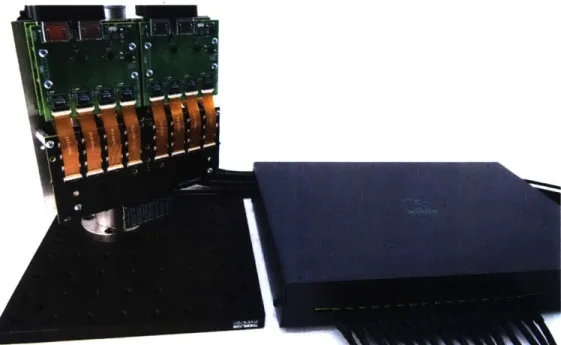
We designed a complete 1000-channel extracellular neural recording system, from probes to headstages to data acquisition, in order to demonstrate the principles of scalable recording system design, and test out new algorithms for spike-sorting with close-packed electrodes, as discussed in Chapter 3. As shown in Figure 2-1, we kept the three parts of this system separate and modular, to enable continuous development of each component.
Figure 2-1: Photograph of 1000-channel data acquisition system. Headstages (green circuit boards, left) and probe interface circuit board (black circuit board, left) are mounted on a metal plate attached to a linear translation stage, in the configuration that would be used for a recording experiment (there is no probe attached to the interface board in this figure). Flat flexible cables (orange), each with 33 conductors, connect the headstage amplifiers to probe recording channels. 16 HDMI cables carry digital I/0 and power between the headstages and the data acquisition module, packaged in the metal enclosure, right. Not shown is a visualization computer, which would be connected to the data acquistion module over ethernet cables.
2.2.1 System Design
Probes
We developed a close-packed silicon microelectrode technology that enables a tight con-tinuuni of recording sites along the length of the shank. This arrangement thus enables tetrode-like spatial oversampling continuously running down the shank, so that sorting of spikes recorded by such densely packed electrodes can be facilitated for all the sites of the probe simultaneously. We use advanced lithography tools to create these close-packed ar-rangements in a scalable fashion, demonstrating probes with 1000 electrode pads situated on
5 shanks with 200 recording sites per shank (Figure 2-2). A key challenge with traditional
silicon electrode designs has been that wiring to the recording sites occupied a large fraction of the available shank area. This is problematic because scaling up the number of recording
sites forces the shank geometry to widen, placing an upper bound on the number of sites practical for a single shank of a given width. We here reduced the wire geometry, and thus the overhead that the wiring places on the shank width, by creating subinicron wires with high-speed electron beam lithography (EBL), which enables us to create feature sizes of 200 nnm. The accuracy of this technology also enables a 1.5 p in space between individual recording sites, resulting in a close-packed design in a simple single-metal layer process.
A
B
C
Figure 2-2: Close-packed electrodes manufactured on a thin silicon substrate. A. Photo of a close-packed 1,000-channel probe, shown with penny, for scale. The sensor area is outlined by the dashed orange line, and the silicon extends to the rectangular region below the penny where wirebonds connect the silicon to the printed circuit board (PCB). The rest of the PCB's area is devoted to wiring and connectors for routing the signals to neural amplifiers on a separate PCB. B. SEM image of sensor area of a 2-shank, 240-channel probe, with electrode sites false-colored gold. Electrode sites are 9 pim x 9 lim, with 11 1111 spacing center-to-center.. Electrode shanks taper from 120 p1m wide at their widest point to 57 p"m at the bottom row of electrodes. The silicon substrate beneath the sensors is 15 pms thick .
C. SEM image of a cross-section of a silicon probe. with different material layers highlighted
in false-color: gold for gold, cyan for silicon dioxide, and blue for silicon. The gold layer is
150 nm thick. The opening in the insulating silicon dioxide for the gold electrode site, right,
is 10 Ims. The gold wiring encapsulated in silicon dioxide, left, is 200 in wide on a 400 n1 center-to-center spacing.
We adapted a hybrid lithography method. using electron beani lithography (EBL) to
26
write the fine structures on the probes (for example, the finest wiring along the implanted component) while using classical MEMS fabrication techniques for larger structures (for example, the wirebond pads, the non-fine wiring, and the cutout of the probes). Breaking the metallization into these two steps allows us tO utilize the submicron capability of electron beam lithography for dense wiring on the shanks, while maintaining the high throughput of optical lithography to define the less dense wiring outside of the shanks. The highest wiring density is required when routing alongside the recording sites, because here the shank needs to accommodate both the wiring as well as the recording sites, while remaining as narrow as possible to reduce brain displacement or damage. Once the wiring leaves the shank and enters the main body of the probe, significantly more space is available and the wiring pitch can be relaxed, and transitioned to optical lithography. Overall, a 150 mm wafer required about 4 to 5 hours of EBL tool time to complete, with approximately 6000 recording sites spread across a variety of different probe styles of 64, 128, 256 and 1000 channels.
Headstages
We designed custom headstages to amplify and digitize signals between our custom probes and data acquisition system because no commercially-available system offered the density or flexibility to work with our hardware. Headstages employ specially designed neural amplifiers because the signal recorded from extracellular electrodes is small and weak (as sensed at an electrode site, spikes are often less than 100pV peak amplitude, with an impedance greater than 100 kQ at 1 kHz). These weak signals are very sensitive to noise pickup from many sources (e.g. conductive coupling from muscle activity, capacitive coupling from nearby electrical equipment, and inductive coupling from power lines). This places constraints on the distance amplifiers can be placed from the electrodes and the design of recording circuits. Fortunately, the principles of amplifier design for recording neural signals and PCB layout for mixed signal devices are well known[5], and headstages can be designed with commercial, off-the-shelf (COTS) components.
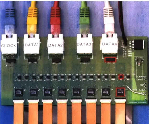
While designing our first generation headstages, we focused on understanding mixed-signal circuit design, defining the special needs of a 1000-channel system, and producing something with which to test our complete signal chain. In this generation, we produced
I
I
'low , OWW - I ~ rix
Figure 2-3: First generation 512-Channel signal-conditioning headstage. Utilizing 16 32-channel analog neural amplifiers (bottom red box) positioned on front and back of
PCB. A 16 bit, 1 MS,/s analog-to-digital converter (ADC. middle red box) reads in the
multiplexed analog data from the neural amplifier, and outputs single-ended pulses to a differential converter (top red box). Clock pulses are transmitted differentially from the data acquisition module and converted to single-ended signals to control to the amplifiers and ADCs. Standard nixed-signal PCB layout techniques are used to prevent crosstalk from the digital signals on the analog recordings. The headstage circuit board is 6 inches wide.
512-channel headstages that were just 6 inches wide, using 8 32-channel analog multiplexed neural amplifiers (Intan RHA2132) on both the front and back of the board, connected to the probe interface board over flat flexibles cables (FFCs) with a 0.3 mn wire pitch (Figure
2-3). We used mixed-signal circuit design techniques to achieve an input-referred noise of 3
pV per channel, measured through the complete data acquisition system, very close to the
amplifier's intrinsic noise level of 2.5 yV.
The second generation of headstage design focused on usability improvements. We
adopted a iore modular design, using 128-channel headstages with a newer anplifier design
(Intan RHD2132) with built-in ADCs and greater functionality. Our headstages included
28
I
auxiliary connections for analog input, which were used to synchronize amplified patch-clamp signals and experimental metadata during colocalized recordings (Chapter 3). We also used the headstages in a custom electroplating system to reduce the impedance of our
electrodes. The headstages switch between providing electroplating current to the
elec-trodes and measuring the resulting impedance, enabling feedback-controlled specification of impedance. Other usability improvements included mounting points on the circuit boards, indicator LEDs, and power switches, which proved very useful when the headstages were used for colocalized recordings, relied on daily in a complex experimental procedure.
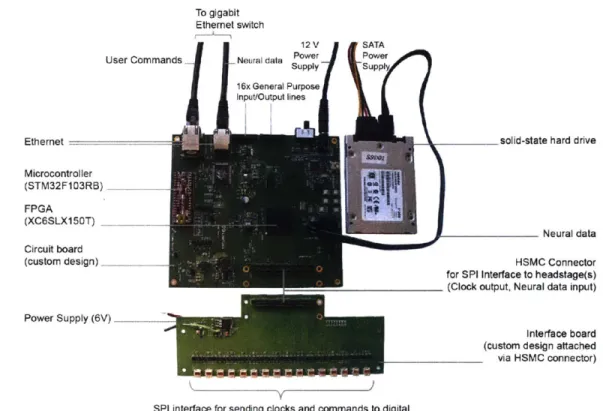
Data Acquisition
We built a minimalist DAQ module (Figure 2-4) centered around an FPGA (Spartan-6 LX150T, Xilinx, Inc.) that acquires neural data directly from analog-to-digital converters downstream from amplifiers headstages. Existing DAQ systems commonly rely on conven-tional desktop or server machines for data storage. This works well for small numbers of neural DAQ channels, but at higher channel counts a direct communication design based on FGPAs, such has been implemented for massive DAQ projects in high energy physics[6] and astronomy[7], offers several advantages. Writing data directly to hard drive yields a cost savings, as well as a reduction in complexity. Unlike a CPU, on the FPGA each of the data pathways (connecting sensors, hard drive, and Ethernet) are processed in parallel on dedicated circuitry and have no effect on each other's performance. With no operating system adding a source of complexity and non-determinism, basic performance guarantees of an FPGA are straightforward and do not require sophisticated techniques such as real time kernels. Furthermore, an FPGA, once programmed, employs dedicated logic for each of the system tasks such as acquiring and storing data, yielding exceptionally high data through-put due to the intrinsically parallel structure of how data streams can flow. Of course, this architecture could also be implemented in an application specific integrated circuit (ASIC), but FPGAs are off-the-shelf parts, reducing entry costs to create such devices, while also allowing for easy modification of the firmware and implemented circuits.
Each of these modules can acquire data from 1024 channels at 16-bit depth at 30 kHz. The module stores data directly to an attached SATA storage device and simultaneously
distributes a copy of the neural data over a high speed (1 Gb/s) Ethernet wired network, e.g., to a visualization computer for real-time inspection of neural data. The module is controlled remotely by sending basic user commands, e.g., start or stop recording, over the network from the visualization computer. In addition to neural data, the module can store experiment protocol information or experimental data, e.g., triggers from beam breaks or for laser pulses, accessible by the experimenter and useful for coordinating overall system operation. To assist in reconstructing a complete neural recording data set from multiple modules being used in the same acquisition session, each module tags neural data with meta-data such as hardware identifiers and time stamps. The total data rate to acquire 1024 channels of data, including auxiliary data, meta-data and zero padding, is 122.88 MB/s. At this data rate, a 512 GB hard drive, for example, can store up to 70 min of data from 1024 channels.
Our implementation uses 62% of the available resources of the FPGA chosen. With the unutilized resources it may be possible to add further functionality such as real-time lossless compression, which can enable both a higher data transmission density and an increased storage capacity (and thus improved utilization of the hard drives). In principle the duration of recording by the data acquisition system could be made longer by increasing the size and/or number of hard drives. Multiple independent SATA controllers could be embedded in the FPGA firmware to support multiple attached hard drives (for instance, our implementation allows two attached hard drives), allowing for increased recording times or for preventing data loss after a drive failure via redundancy. Furthermore, upgrading the embedded controller to operate at SATA II for faster data write speeds (i.e., 3 Gb/s) to, for example, accommodate more than 1024 channels of neural data, would be straightforward. In addition, extremely low latency, closed loop control experiments are feasible if control logic is implemented within the FPGA[8]. Furthermore, it is conceivable that analysis could be performed on the FPGA, with the level of difficulty depending on the complexity of the algorithm. Notably, spike sorting on the FPGA, and only storing the resultant spike information, could in principle yield a dramatic reduction in the rate of output data by several orders of magnitude[6, 9].
To gigabit Ethernet switch
12 V SATA
User Commands Neal dt Power
16x General Purpose
Input/Output lines
WEE
solid-state hard drive
Neural data
HSMC Connector
for SPI Interface to headstage(s)
(Clock output, Neural data input)
Interface board (custom design attached via HSMC connector)
SPI interface for sending clocks and commands to digital
neural amplifier chips and receiving 16-bit neural data
Figure 2-4: Implementation of direct communication design of data acquisition (DAQ) module. Photograph of the acquisitioni module with key parts labeled. The
field-programmable gate array (FPGA) board measures 15cm x 16 cm x 2 cm. Ethernet Microcontroller (STM32F103RB) FPGA (XC6SLX150T) Circuit board (custom design) Power Supply (6V) maam-a-a-a-a-a-a-a-en-a-a-=-a.--=weswa
2.3
Discussion
We have developed a 1000-channel neural recording system optimized for scalability. Our probes utilize state-of-the-art fabrication tools to maximally cover the surface of the probe with recording sites. Headstages leverage small neural amplifiers chips to pack a large amount of signal conditioning capacity in a small area, which is important for signal integrity and usability. Our data-acquisition systems are contained in a purpose-built custom module to reduce cost and minimize the complexity of using multiple modules simultaneously. All of these components can leverage the continuous development of microelectronics fabrica-tion tools to increase channel counts, decrease system size, and expand the computafabrica-tional capabilities of the system.
One particular lesson we have learned from extensive user testing is that it's very im-portant to make good choices for the physical definition of interconnects between modules. Because sticking with these choices is critical to maintaining modularity, they can persist much longer than any other design choice in the system. We chose to use FFCs with zero-insertion-force (ZIF) connectors between the probes and headstages because they have very dense wiring and mechanically decouple the two systems, be we found it annoying to connect so many FFCs when swapping probes in and out. If we were to respecify this interconnect, we would use connectors that are high-channel-count as well as high density, and mount them on custom flexible PCBs to maintain the mechanical affordances of the system. Like-wise, between the headstage and data acquisition system we would employ fewer cables, by serializing outputs. We use the twisted pairs of our HDMI cables to carry differential signal outputs, but they are much lower bandwidth than the cables are rated for. With serializa-tion, all of the data for a 1000-channel recording could be carried over a single HDMI cable. Both of these improvements could be achieved with COTS components, minimizing the cost and complexity of the implementation.
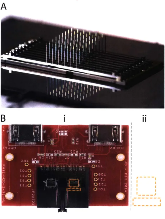
Yet for order-of-magnitude improvements in system capacity, we will need to make some changes to the architecture. Probes and amplifiers will require tighter integration, no longer considered to be separate modules. Probes will become three-dimensional, in order to im-prove spike sorting (see Chapter 3) and more fully map neural circuits. Amplifiers will be
directly attached to neural probes, leveraging finer wire widths and better packaging op-tions, as shown in Figure 2-5. Looking ever further ahead, we can even use more advanced amplifier architectures that achieve greater density[cite], and even fabricate amplifiers on the same silicon as the probes[2], a strategy that should scale to tens or hundreds of thousands of channels.
The modular, parallel architecture of the data acquisition system will enable scaling by unit increments of 1024 channels, to an arbitrarily large number (Figure 2-6). This paral-lelism splits up the original data, and the data can if desired later be recombined on the analysis side, during readout from the individual units. This simply requires synchronization across individual DAQ modules, which can be achieved with a shared clock pulse. Visual-ization could take place on multiple computers if desired, each receiving a number of data streams from several modules. Data analysis will be decentralized as well, on acquisition systems, so that results can be pooled with significant data compression.
A
B
.ii
IVI
Figure 2-5: Methods for scaling and integrating probes and headstages. A) 3D probe array. B) Silicon probe with bare silicon amplifier chips (top left dashed box) wire-bonded directly to silicon interposer. Using bare silicon amplifiers dramatically reduces
amplifier area (coipare to size of packagedl neural amplifier, top right daslied box) and wiring size (compare bottom two dashed boxes). Digital I/O and power lines are connected to red headstage PCB via wirebonds.
Workstation
Compute servers
Network switch
Acquisition modules & hard drives
Interface board Headstage Amplifiers & Digitizers Electrode array
H>
IT
Figure 2-6: Schematic for using multiple data acquisition systems in parallel.
Bottom to top - signals from electrode array are split into separate pipelines that feed
through headstages and into acquisition modules which can record and preprocess the data.
A network switch connecting all of the acquisition modules allows a single workstation to
communicate with all parts of the system, which may include extra nodes for computation.
I
2.4
Methods
2.4.1
Probes
The fabrication of our devices was carried out on 150 mm silicon-on-insulator (SOI) wafers (Ultrasil Corp., Hayward CA). The top ("device") layer thickness of the SOI wafer defines the probe shank thickness, and therefore a wide range of precise thicknesses is possible. We chose a thickness of 15 [ m, comparable to typical silicon-based electrodes [16]. The process
consists of two key parts: first, the formation of the insulated metal wiring and exposed metal pads, and second, the deep reactive ion etching (DRIE) steps that define the shape of the probe and the thin shanks. Fabrication starts with deposition of an insulating dielectric. We then use electron beam lithography to define the recording sites and high density metal wiring. Exposure and development of electron beam lithography resist is followed by metal evaporation of a film stack of 10 nm Ti, 150 nm Au, and 5 nm Ti, where the Au is the conductor and the Ti serves as an adhesion layer to the SiO2. After a liftoff procedure in acetone, a second metallization step follows, using standard optical (UV) contact lithography with a 2 p m feature size. Metal for liftoff is deposited by evaporating a 10 nm Ti, 250 nm Au, and 5 nm Ti film stack, and metal liftoff is again performed in acetone. After the metal processing on the front side, an SiO2 layer is deposited and patterned to expose only the recording sites while insulating the wiring. To pattern the dielectric layer and to open up the electrode and wirebond sites, we again use a combination of EBL and optical lithography. We first pattern and etch open the recording sites with precisely aligned EBL to achieve submicron alignment accuracy to the recording sites, with 1 to 2 P m spacing between them. Next, the large wirebond pads are patterned and etched with optical lithography.
Finally, we etch out the probe shapes using two deep reactive ion etch (DRIE) steps, once on the front side of the probe, and then again on the backside. The dual-sided DRIE etching allows us to create shanks of precisely defined thickness, as determined by the SOI wafer, and also precisely defined shank outlines, a s determined by lithography. The parts of the probe that are not going to be implanted can remain at the original wafer thickness, which facilitates handling and packaging. A portion of the shanks themselves can also remain at full wafer thickness if those sections will not enter the brain. This can help to reduce space
constraints during in vivo use and enabling a better visibility during the probe insertion into the brain, while avoiding unnecessarily long thinned shanks, which can bend due to thin-film stress. We have fabricated thin shanks with lengths up to 7.5 mm (at a thickness of 15 P m), but, we expect more careful stress balancing is needed for shanks with a more aggressive aspect ratio (either longer than 7.5 mm or thinner than 15 p m).
To acquire neural signals recorded with the probes, we need to package and connect the probes to electronic amplifiers and digitizers, which are commonly referred to as "headstages". The purpose of the packaging is to provide the intermediary routing between the silicon probe and the headstages, and to protect the fragile silicon shanks by providing a mechanical body for handling. Both of these goals are achieved through the use of printed circuit boards (PCBs). We directly attach the probes onto a PCB and connect to the probe's wirebond pads using a gold ball bonder. To allow wirebonding, the PCB has an electroless nickel immersion gold finish (ENIG). We used a multilayer PCB to achieve a dense routing of the signals (10 layers, with 8 inner routing layers and 3 mil feature sizes, Advanced Circuits, Aurora CO). These specifications allow us to connect the very densely laid out wirebond pads on the 1000 channel probe. However, for the PCB design, the bottleneck in the layout is the diameter of the via that connects the surface pads to the individual routing layers (in our design, a 14 mil diameter ring with a 4 mil via hole). These dimensions constrained our wirebond pad pitch to 10 mil. Using a more aggressive (albeit more expensive) PCB technology can help reduce this pitch as needed, enabling either higher channel counts or reducing the chip size. However, with our choice of dimensions we find an adequate tradeoff between PCB cost and the required probe size for 1000 channels. Because the metal we wirebond to on the probe is thin, with only 250 nm of gold, and because it sits on top of a relatively thin layer of 1 p m SiO2, choosing the right wirebonder settings is important to avoid cratering through the oxide and short circuiting the pads. Typical chip pads in the semiconductor industry often employ a much thicker metal and dielectric stack that is more robust. However, by appropriately choosing the wirebonding conditions (in our case, power and time settings), we found that we can reliably bond all 1000 channels without any pad damage. The routing across 8 layers in the PCB then takes place below the silicon chip. While lower channel count probes do not require this many PCB layers, we fabricated them
on the same PCB run and therefore benefit from the reduced amount of space needed for PCB routing. The 64 channel probe seen in Fig. 10 illustrates the small form factor that can be achieved. Once the PCB wiring exits the immediate area around the probe, the wiring density can be relaxed as we route towards Flat Flexible Cable (FFC) connectors (Molex 5025983393) that attach to the amplifier headstages. We chose FFC connectors for this design because of the low cost and the ability to use flexible cables that help to mechanically decouple the probe from the headstages. But, many other high-density connector types exist, and they can readily be substituted for the FFC connectors. The additional space overhead
is acceptable for the acute, head-fixed in vivo experiments that we are targeting with this technology, for example for mice in a head-fixed virtual reality environment [23]. Overall, the parasitic capacitances are small ( 10 pF) when compared to the electrode impedance
(500 pF).
2.4.2
Headstages
PCB layout utilized mixed signal layout techniques in a 4-layer board to prevent crosstalk from digital I/O lines to amplifier pickups. This included using split ground planes, ground vias for current return paths when signals switched layers, and differential signaling wherever possible. Noise was measured by connecting a probe to the amplifier and immersing it in saline to achieve realistic input impedance. Digitized signals from the data acquisition system were analyzed and RMS noise values were extracted.
2.4.3
Data Acquisition
&
The FPGA core architecture is shown in Figure 2-7. To transfer data onto and off the FPGA, we took advantage of built-in, high-speed, serial transceivers, and implemented the industry standard SATA 1 interface (187.5 MB/s) in the FPGA itself as a SATA core. This allows the module to store data directly to an attached SATA storage device at data rate sufficient to capture 1024 neural recording channels. In addition, a copy of the neural data can be distributed over a network for relay to a visualization computer. To achieve 1 Gb/s data rates over Ethernet, neural data is encapsulated as UDP packets by the Ethernet/UDP
II
core. This core interfaces with an onboard Ethernet controller (Marvell MV88E1 111, which implements an Ethernet PHY layer).
50 MHz Microcontroller Ethernet
Os. TCP/IP User Commands
a 'Chip (TCP)
Spartan-6 FPGA
Clock Managers o ntrace ...
SPI control
---Headstage(s) Acqaisition Control GPOs.
r .C Core B. tt
(DAQ) Core LEI
-LEDs
...
1K..
...
DDR3 . Memory FIFO (64 KB) LW ... 150 MHz GA-Etene EthernetA Transceive Core FIFO (64 KB) CoreY Neal Data
KEY
__)h _ Neural Data --- * 32-bit commands and cortros Miscellaneous
Figure 2-7: Block diagram of the FPGA circuitry. The programmable FPGA circuitry implements a DAQ core to interface with headstages and add meta-data, a SATA core for direct-to-drive data storage, an Ethernet/UDP core for high-speed data transmission over Ethernet, and a Control core containing of a bank of registers for controlling the system. One gigabyte of DDR3 memory buffers acquired data before it is stored to hard drive. The TCP protocol is implemented outside of the FPGA using a separate microcontroller.
The 1024 channels of data are here brought on board using 32 front-end neural amplifier digital-output chips (Intan Technologies Inc., RHD2132). Each chip is capable of 32 channels of amplification and digitization, and the individual SPI signals from each chip are aggregated on a simple interface board. The DAQ core includes drivers to communicate over a low-level SPI bus protocol to individual chips (according to the RHD2132 specification sheet), higher-level drivers to initialize the chips and acquire data, and an aggregation layer to combine data from all of the chips and make this aggregate data available to other cores through a RAM interface. In addition to sampling the 32 input channels of each chip, the core allows access to a digital-to-analog waveform generation circuit (useful for electrode impedance measurements), auxiliary analog inputs, and the full set of SPI controllable features of the Intan chip.