Distributed Switch Circuits for High Voltage Pulse
Applications
by
John Israel Rodriguez
S.B. in E.E., Massachusetts Institute of Technology (1997)
Submitted to the Department of Electrical Engineering and Computer
Science
in partial fulfillment of the requirements for the degree of
Master of Engineering in Electrical Engineering
at the
MASSACHUSETTS INSTITUTE OF TECHNOLOGY
February 1999
@
John Israel Rodriguez, MCMXCIX. All rights reserved.
The author hereby grants to -MIT permission to reproduce and
distribute publicly paper and electronic copies of this thesis document
in whole or in part, and to grant others the right to d
SSACHUSEOFTECHN
ENGQ
.
- - -
. . .'V . . . .... .-- .. .' . . .' . . .' .
6partment of Electrica Engineering and Computer Science
September 24, 1998
Certified by.
Chathan M. Cooke
Principal Research Engineer
z X'thes Supervisor
. . . .
Arthur C. Smith
Accepted by...
Chairman, Department Committee on Graduate Students
Author
S INSTITUTE
Distributed Switch Circuits for High Voltage Pulse
Applications
by
John Israel Rodriguez
Submitted to the Department of Electrical Engineering and Computer Science on September 24, 1998, in partial fulfillment of the
requirements for the degree of
Master of Engineering in Electrical Engineering
Abstract
A distributed switch, in this work, is a "super switch" device formed by cascading individual switches in series. Series distributed switches can be used in situations where single solid state devices would otherwise fail to provide enough voltage block-ing capability. Because the parasitics inherent in these circuits can hinder faster switching action, finding ways to overcome these parasitic effects requires knowledge of how they influence a cascaded switch. Models that describe the impact of the parasitic inductance and capacitance in these circuits are presented and studied. The approach taken is to realize that parasitics in a distributed switch form uniform LC ladders similiar to those used for modeling transmission lines by lumped approxima-tion. As a result, the total circuit forms a switched LC ladder network. The natural LC structure of these switched networks are shown to share many interesting proper-ties with classical lumped LC lines. Furthermore, when the parasitic elements of the line dominate the distributed switch response, the introduction of a defined uniform delay in the firing pattern of the individual switches can be used to enhance the speed of response. Experimental results to support these claims are presented for circuit
responses in the microsecond to nanosecond regimes. Thesis Supervisor: Chathan M. Cooke
After ten years of apprenticeship, Tenno achieved the rank of Zen teacher. One rainy day, he went to visit the famous master Nan-in. When he walked in, the master greeted him with a question, "Did you leave your wooden clogs and umbrella on the porch?"
"Yes," Tenno replied.
"Tell me," the master continued, "did you place your umbrella to the left of your shoes, or to the right?"
Tenno did not know the answer, and realized that he had not yet attained full awareness. So he became Nan-in's apprentice and studied under him for ten more years.
Acknowledgments
I wish to thank Dr. Chathan Cooke for suggesting this research topic and guiding me at every step of its development. I have always been amazed by his keen sense of intuition and savvy for engineering. Needless to say, his supervision and talents were instrumental to the completion of this thesis. He is a continual source of motivation to me and I am a better engineer because of him.
I am also deeply indebted to Professor Jeffrey Lang, my academic advisor. Whether Jeff realizes it or not, there were times when I was convinced he was the only person in the department who believed in me. In fact I owe my start as a TA in 6.002 Circuits and Electronics to him personally. The times I spent teaching under him, as well as Professors Wilson, Schlecht and Ram are perhaps the memories I treasure most about MIT. My experiences as a TA have complemented my education in ways that course work simply could not. The reason for this is simple; it's the students. Simply put, they are "amazing". Each unique in his or her own way and on the whole unbelievably diverse. I pray for their continued success and I cherish deeply the time I have spent coming to know and befriend them. I hope some of them will say the same.
Warmest thanks to Anne Hunter for rescuing me from those numerous department related jams I'm always finding myself in. But more importantly, for the pivotal role she played in my admission to the Masters of Engineering program. "Big" John Sweeney, for all of the equipment he lent me throughout my research, and always saying to me, "GO HOME!". And Jaydeep Bardhan, technical writer extraordinare, for his numerous suggestions and extensive editing of my thesis.
Also, my unending gratitude to those individuals I often owe my very sanity to. My colleagues Tim Denison, Steve Paik and Ketan Patel who listened to my incessant prattling about distributed switches. The Park Street Gang for their prayers and continual support. Kofi Aidoo, who I am convinced is just another aspect of myself, although, I'm sure he thinks it's the other way around. My roommate and long time friend, Carl Hibshman, who has come through for me time and time again. He is quite conceivably the most generous person I know. Did I mention he also proofread and corrected earlier drafts of my thesis, just because?
And of course, my caring family who never pressured me into doing something I did not want, but through love and affection supported me with all they had at times. I just want them to know, we did it.
En Domino Speas Mea.
Contents
1 Introduction 15 1.1 The Problem . . . . 15 1.2 Parameters of Interest . . . . 16 1.3 A pproach . . . . 17 1.4 Thesis Outline . . . . 17 2 Lumped LC Lines 18 2.1 Introduction . . . . 182.2 Modeling Lumped LC Lines . . . . 18
2.3 Previous Work . . . . 19
2.3.1 ABCD Matrices . . . . 20
2.3.2 Characteristic Impedance and Propagation Delay . . . . 21
2.3.3 Rule of Thumb for Selecting the Number of Cells . . . . 22
2.4 MATLAB Simulation . . . . 23
2.4.1 Scaling by T = v/LC . . . . 23
2.4.2 Scaling by Z, = L.... . . . . 25
2.4.3 Load and Source Mismatching . . . . 26
2.4.4 N -effects . . . . 29
3 Uncharged, Switched LC Lines 34 3.1 Introduction . . . . 34
3.2 Modeling Uncharged, Switched LC Lines . . . . 34
3.3 Distributed Switch Triggering . . . . 36
3.4 PSPICE Simulation . . . . 37
3.4.1 Wave Propagation(K) . . . . 38
3.4.2 Internal Stresses . . . . 39
3.4.3 N Effects . . . . 43
4 Precharged, Switched LC Lines 47 4.1 Introduction . . . . 47
4.2 Modeling Precharged, Switched LC Lines . . . . 47
4.3 PSPICE Simulation . . . . 48
4.3.1 Wave Propagation(K) . . . . 49
4.3.2 Impedance Matching . . . . 50
4.3.3 Switch Stresses . . . . 57
4.3.4 N -effects . . . . 60
4.4 A Comparison of Output Behavior . . . . 65
5 Experimental Validation of Models 68 5.1 O verview . . . . 68
5.2 Design and Implementation . . . . 69
5.2.1 Hardwired LC Line . . . . 69
5.2.2 Precharged Distributed Switches . . . . 70
5.3 Experiment I: Fixed LC Line . . . . 79
5.3.1 Captured Waveforms . . . . 79
5.3.2 Actual Output vs. Simulated Output . . . . 81
5.4 Experiment II: Slow Precharged Switch . . . . 82
5.4.1 Captured Waveforms . . . . 83
5.4.2 Actual Waveform vs. Simulated Waveform . . . . 87
5.5 Experiment III: Medium Precharged Switch . . . . 93
5.5.1 Captured Waveforms . . . . 93
5.5.2 Actual Waveform vs. Simulated Waveform . . . . 95
5.6.1 Captured Waveforms . . . . 5.6.2 Discussion . . . . 6 Conclusions 6.1 Summary . . . . 6.1.1 The Problem . . . . 6.1.2 Approach . . . .
6.1.3 Simulation Based Results . . . .
6.1.4 Experimental Results . . . . 6.2 Future Directions . . . .
6.2.1 Modeling . . . .
6.2.2 Variations . . . ..
A Matlab Code
A.1 Lumped LC Line (LCline.m) . . . .
A.2 Parameters (params.m) . . . .
B PSpice Netlists
B.1 Uncharged Uniform Switch . . . . B.2 Precharged Uniform Switch . . . . B.3 Precharged Tapered Switch . . . . C Tapered Switch Stresses
D L and C Selection Plots
E TTL FIDT Circuit
E.1 Theory of Operation . . . .
E.1.1 Shift Register . . . .
E.1.2 555 Timer . . . .
E.1.3 Pulse Generation . . . . E.2 Timing Diagrams . . . .
99 102 107 107 107 107 108 108 110 110 111 112 112 118 120 120 121 122 124 126 128 128 128 129 130 132 . . . . . . . . . . . . . . . . . . . .
F Additional Information 134
F.1 GA301A Thyristor Switch ... 134
F.2 PE-64973 Pulse Transformer . . . 134
G PE-64973 Pulse Transformer Characterization 137
G.1 Transformer Testing . . . 137 G.2 Transformer Responses . . . 138
H GA301 Device Characterization 140
H.1 Trigger Scheme Testing . . . 140 H.2 M easured Data . . . . 141
List of Figures
1-1 Switch Parasitics . . . . 16
2-1 L -cell . . . . 18
2-2 Lumped LC Line . . . .. 19
2-3 T Scaling on the output of various 10 stage LC lines . . . . 24
2-4 Z, Scaling on the output of various 10 stage LC lines . . . . 25
2-5 Output of a 10 stage LC line Driven by a Unit Step when Road is matched and R, is mismatched . . . . 26
2-6 Output of a 10 stage LC line Driven by a Unit Step when Rloa=d RS = 2Z, or .5Z . . . .. 27
2-7 Output of a 10 stage LC line Driven by a Unit Step when Road = 2ZO or .5ZO but R, = 0 . . . . 28
2-8 Discretization Effects of a Double-Matched, Uniform LC line: N=1,2,4,8 29 2-9 Unit Step Response of a Double-Matched, Uniform LC line: N=50 . . 30
2-10 Output Overshoot of a Double-Matched, Uniform LC line vs. N . . . 31
2-11 Output Rise Time of a Double-Matched, Uniform LC line vs. N . . . 32
2-12 Output Delay of a Double-Matched, Uniform LC line vs. N . . . . 33
3-1 Uncharged Switch Model . . . . 35
3-2 Uncharged, Switched LC Line Model . . . . 35
3-3 Fixed Inter-Switch Delay Triggering Scheme . . . . 37
3-4 Voltages in a Uniform Uncharged Switch: R, = RI = Z0, N = 5, K = 0 38 3-5 Voltages in a Uniform Uncharged Switch: R, = RI = Z0, N = 5, K = 1 39 3-6 Peak Positive Capacitor Voltage vs. K . . . . 40
3-7 Peak Negative Capacitor Voltage vs. K . . . . 41
3-8 Peak Positive Inductor Current vs. K . . . . 42
3-9 Peak Negative Current vs. K . . . . 43
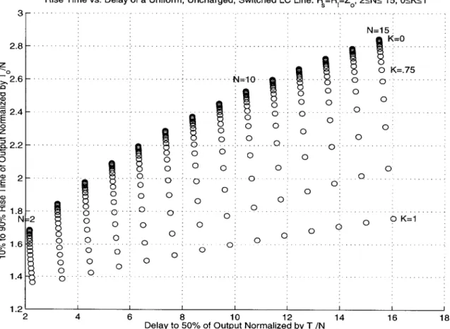
3-10 Rise Time vs. Delay of Uncharged LC Line Normalized by T . . . 44
3-11 Single L-cell equivalence for Large N . . . . 45
3-12 Uncharged Switched, Transmission Line Model . . . . 45
3-13 Rise Time vs. Delay of Uncharged LC Line Normalized by T . . . . 46
4-1 Precharged Switch Model . . . . 48
4-2 Precharged, Switched LC Line Model . . . . 48
4-3 Voltages in a Uniform Precharged Switch: R = R, = Z0, N = 5, K = 0 49 4-4 Voltages in a Uniform Precharged Switch: Rt = R, = Z, N = 5, K = 1 50 4-5 Voltages in a Uniform Precharged Switch: Rt = .5Z, R, = Z0, N = 5,K = 0 . . . . 51
4-6 Voltages in a Uniform Precharged Switch: Rt = .5Z, R, = Z0, N 5, K = 1 . . . . 52
4-7 Voltages in a Uniform Precharged Switch: Rt = 0, R, = Z0, N = 5,K = 0 . . . . 53
4-8 Voltages in a Uniform Precharged Switch: Rt = 0, R, = Z, N = 5,K = 1 . . . . 53
4-9 Output of Previous Switches (Extended Time Axis): Rt = 0, R1 = Z ,N = 5,K = 0,1 . . . . 54
4-10 Voltages in a Tapered Precharged Switch: 5Rt = R, = Ze"l(5), K = 0. 56 4-11 Voltages in a Tapered Precharged Switch: 5Rt = R = Ze"l(5), K = 1 56 4-12 Switch Voltages for K=1 . . . . 57
4-13 Maximum Switch Voltage vs. K . . . . 58
4-14 Peak Positive Switch Current vs. K . . . . 59
4-15 Peak Negative Switch Current vs. K . . . . 59
4-16 Rise Time vs. Delay of Precharged LC Line Normalized by To . . . . 60
Limiting Output Behavior of a Precharged, Switched LC Line for K<1 Limiting Output Behavior of a Double-Matched, Precharged, Switched LC Line for K >1 . . . .
4-20 Rise Time vs. Delay of Precharged LC Line Normalized by T.N 4-21 Comparison of Overshoot. . . . . 4-22 Comparison of Rise Times... .. .. .. .. .. .. .. .. .. .
Fixed LC Line Schematic . . . . Precharged Switch Schematic . . . . Biasing Network . . . . Test Setup for Experiment I: Fixed LC Line . . . . Captured Waveforms: Hardwired LC Line . . . . Hardwired LC Line: Actual vs. Simulation for Nominal T, Hardwired LC Line: Actual vs. Simulation for Adjusted T, Test Setup for Experiment II: Slow Precharged Switch . .
Captured Waveforms: Captured Waveforms: Captured Waveforms: Slow Switch, Rt = R = 47Q, K=0 . Slow Switch, Rt = RI = 47Q, K=.75 Slow Switch, Rt = RI = 47Q, K=1 . 5-1 5-2 5-3 5-4 5-5 5-6 5-7 5-8 5-9 5-10 5-11 5-12 5-13 5-14 5-15 5-16 5-17 5-18 5-19 5-20 5-21 5-22 5-23 4-18 4-19
Captured Waveforms: Slow Switch, Rt = 25Q, R = 47Q, K=0 . . . .
Captured Waveforms: Slow Switch, Rt = 25Q, RI = 47Q, K=1 . . . . Captured Waveforms: Slow Switch, Rt = OQ, R, = 47Q, K=0 . . . . .
Captured Waveforms: Slow Switch, R= 00, RI = 470, K=1 . . . . .
Slow Switch: Actual vs. Simulation for Nominal T0, Rt = 47Q, K=0 .
Slow Switch: Actual vs. Simulation for Nominal T, Rt = 47Q, K=.75 Slow Switch: Output vs. Simulation for Nominal T, Rt = 47Q, K=1
Slow Switch: Actual vs. Simulation for Nominal T, Rt = 25Q, K=0
Slow Switch: Actual vs. Simulation for Nominal T, Rt = 25Q, K=1
Slow Switch: Actual vs. Simulation for Nominal T, Rt OQ, K=0
Slow Switch: Actual vs. Simulation for Nominal T, Rt = OQ, K=1 Slow Switch: Actual vs. Simulation for Adjusted T0, Rt = 47Q, K=1
62 63 64 65 66 69 71 73 79 80 81 82 83 84 84 85 85 86 86 87 88 89 89 90 90 91 91 92
Test Setup for Experiment III: Medium Precharged Switch . Captured Waveforms: Medium Switch, Rt = R, = 47Q, K=0 Captured Waveforms: Medium Switch, Rt = R, = 47Q, K=1
5-27 Medium Switch: Actual Output vs. Simulation for Nominal T, K=0 Medium Switch: Actual Output vs. Simulation for Nominal
Medium Switch: Actual Output vs. Simulation for Adjusted Test Setup for Experiment IV: Fast Precharged Switch . . . Captured Waveforms: Fast Switch, FIDT=Ons . . . . Captured Waveforms: Fast Switch, FIDT=lns . . . . Captured Waveforms: Fast Switch, FIDT=2ns . . . . Output Comparison of Fast Switch for FIDT=Ons,lns,2ns Switch Voltages in Fast Switch: FIDT=Ons . . . . Switch Voltages in Fast Switch: FIDT=1ns . . . . Switch Voltages in Fast Switch: FIDT=2ns . . . . Voltage at Pulse Transformer Primaries: FIDT=2ns . . . . . Pulse Transformer Voltages: FIDT=2ns . . . .
T, K=1 96 Tr, K=1 97 . . . . . 98 . . . . . 99 . . . . . 100 . . . . . 100 . . . . . 101 . . . . . 102 . . . . . 103 . . . . . 103 . . . . . 105 . . . . . 106
6-1 Overshoot vs. Rise Time for Precharged Switch: Rt=R1=Z, N=5 C-1 Maximum Switch Voltage vs. K . . . . C-2 Peak Positive Switch Current vs. K . . . . C-3 Peak Negative Switch Current vs. K . . . . D-1 A and 2 Selection Plot for the LC Ladder and Slow SwitchN N D-2 L and C Selection Plot for Medium Switch.... .. .. .. . N N E-i E-2 E-3 . . . . . 126 . . . . . 127
TTL Trigger Circuit Schematic . . . . Fixed Inter-switch Delay Triggering . . . . Simultaneous Triggering . . . . 131 132 133 135 136 F-1 GA301 Thyristor Information . . . .
F-2 PE-64973 Pulse Transformer Information . . . . 5-24 5-25 5-26 93 94 94 95 5-28 5-29 5-30 5-31 5-32 5-33 5-34 5-35 5-36 5-37 5-38 5-39 109 124 125 125
G-1 PE-64973 Test Circuit . . . . 137
G-2 Pulse Propagation: im Coax, Pulse Transformer: Rp,=oo, Rsec=51Q 138 G-3 Pulse Propagation: im Coax, Pulse Transformer: Rpi=51Q, Rsec= o 139 G-4 Pulse Propagation: 1m Coax, Pulse Transformer: Rpi=51Q, Rsec=51Q 139 H-1 GA301 Test Circuit . . . . 140
H-2 TTL Drive, R9=51Q . . . . 141
H-3 TTL Drive, Pulse Transformer, Rg=51Q . . . . 142
H-4 TTL Drive, Pulse Transformer, Rg=51Q1|C=O.1pF . . . . 142
H-5 TTL Drive, Pulse Transformer, Rg=OQ . . . . 143
H-6 Wavetech, Im coax, Pulse Transformer|lRpi=51Q, Rg=OQ . . . . 143
List of Tables
5.1 Hardwired LC Line Component Values . . . . 70
5.2 Precharged Switch L and C Values . . . . 72 5.3 Bias R esistors . . . . 74
5.4 C0st and Corresponding Droop Assuming Worst Case Rterm=0 . . . . 76
5.5 Maximum Repetition Rate, fmax, Assuming a Worst Case Rterm=O . 77
5.6 Rise Times for Fast Switch . . . . 101 E.1 Precharged Switch L and C Values . . . . 129
Chapter 1
Introduction
1.1
The Problem
All solid state switches are limited by the maximum voltage they are capable of
supporting while in their "off" state. Exceeding this voltage can cause a device to conduct prematurely or even destroy it. If a higher voltage switch is desired, a "super
switch" structure can be constructed by cascading individual switches in series. This cascade is referred to as a distributed switch because it forms a switch which is "distributed" in space. Distributing a switch in space provides a means of dividing its voltage requirement amongst the individual devices that comprise it. This makes it possible to achieve a factor of N increase in holding voltage capability, where N is the number of single devices comprising the overall switch.
This higher voltage capability does not come without consequence. Because switches are devices that conduct current, energy must be stored in an associated magnetic field. This implies that each individual switch has a non-zero inductance associated with it. Device leads, for instance, account for this inductance to a first order approximation. Furthermore, if two conducting surfaces are present and insu-lated from each other, then electric fields must also exist, giving rise to capacitance. Such a capacitance exists between the pad to which a device is soldered, and the cir-cuit's ground plane. An illustration of these parasitic inductances and capacitances is shown in Figure 1-1. As a result of cascading individual switches, these inductances
Figure 1-1: Switch Parasitics
and capacitances produce a very regular lumped LC line in which the switches are embedded. When the switching speed of the individual devices is slow compared with the dynamics of the LC line, the response of the system is dominated by the device physics, and the parasitics can be ignored. When the speed of the individual de-vices becomes comparable to the dynamics associated with the LC line, however, the parasitics effects can hinder peak switching action and should be taken into account.
1.2
Parameters of Interest
The behavior of a distributed line structure depends on a number of parameters. In order to understand the response of such a system, these parameters must be identi-fied, and their influence on specific characteristics of the line studied. In particular, it is important to understand how the rise time, delay time, and overshoot of the output as well as the internal stresses are functions of the following parameters:
1. The number of stages or "N effects"
2. The inductance and capacitance of the line 3. Loading effects at both ends of the structure
4. Introduction of a fixed inter-switch delay into the switch firing pattern Solid State Switch Leads H Lp Pads Cp E Ground Plane
The first three parameters apply to all lumped LC line structures, and the fourth parameter applies only to the switched line case.
1.3
Approach
The project began with a review of what is currently known about modeling lumped LC lines. The effects of the previously mentioned parameters were studied in the context of fixed LC line models via a combination of analysis and simulation. These models were later modified to include ideal switch elements to represent the first order behavior of solid state switches, and wave propagation in the cascade was then studied for different fixed inter-switch delays. In both of these cases, the systems were initially at rest; all inductor currents equaled zero and all of the capacitors were uncharged. Next the switched line was precharged in order to simulate how an actual distributed switch would behave in a high voltage pulse circuit. Lastly, experiments were conducted on three different distributed switches in order to verify the accuracy
of the simulations and modeling.
1.4
Thesis Outline
The remainder of this thesis proceeds in stages. Chapter 2 forms the groundwork, starting with classical lumped LC lines. Their similarities to transmission lines, as well as their uses for modeling transmission lines, are discussed. Many important properties of these structures are also reviewed. Chapter 3 then introduces the un-charged, switched LC line by modifying the classic LC line to include switches. The behavior of this distributed switch is studied and compared against its classic coun-terpart. Chapter 4 discusses the advantages of "precharging" the switched line and how the precharging process affects the switch behavior. Chapter 5 documents the experiments used to validate the simulation models. Conclusions are drawn in Chap-ter 6 and areas for further research are suggested. Finally, Appendices A - H provide ancillary information relating to this research.
Chapter 2
Lumped LC Lines
2.1
Introduction
The topic of LC lines is one that has a rich history in electrical engineering. LC ladder networks have traditionally been prized for their uses in filtering as well as modeling the behavior of lossless transmission lines by lumped element approximation[5, 7]. LC lines serve as a starting point for understanding the behavior of distributed switches because they make up the structure in which the individual switches reside.
2.2
Modeling Lumped LC Lines
A variety of lumped element models exist for the purpose of describing transmission lines. One commonly used model consists of a series inductance L and a shunt ca-pacitance C to ground as seen in Figure 2-1 below. Because of its shape this model
Ii 12 L 2 A B Vi C V2 A' B' Figure 2-1: L-cell
is referred to as the L-cell for an LC line. The L-cell is an "unbalanced" model in the sense that it lumps all of the inductance on one side of the shunt capacitance. Other models exist that correct this asymmetry, such as the T-cell model, which does so by splitting the inductance equally on each side of the capacitance, or the 7r model, which chooses to split the capacitance instead. The accuracy of these various models is similar regardless of which particular model is used[3].
A lumped element line can be modeled by cascading N elementary L-cells to
produce the two port network shown in Figure 2-2. Traditionally, the total inductance and capacitance of the line is divided evenly amongst the N cells for the purposes of approximating transmission lines (this convention is followed throughout this work). Each cell represents a discretization of the space variable for a true transmission line. Increasing the number of cells creates a greater resolution of the true behavior in space. This model is essential to understanding how distributed parasitics affect the propagation of waveforms through a lumped line structure.
11 IN Rsource A L/N L/N UN UN L/N B - Rload ++ 0-- - -- /VYY _6 + VoU I (t) VI C/N C/N C/N C/N C/N VN A' B'
Figure 2-2: Lumped LC Line
2.3
Previous Work
Although lumped element models are mentioned frequently in literature there are few publications that discuss the number of cells needed to accurately model a transmis-sion line[3, 8]. There are three major criteria that are traditionally investigated for demonstrating how the number of stages influences the behavior of a lumped LC line.
2. Relative Error on the Propagation Delay To and Characteristic Impedance Z, 3. Relative Error on the Natural Frequencies
The first and second criteria are intimately related and briefly discussed here because they are germane to the development of this thesis. The reader is referred to the appropriate references for further discussion of the third metric[3, 8].
2.3.1
ABCD Matrices
One way to describe the behavior of an L-cell is with its ABCD matrix. ABCD matrices provide a convenient method of describing the input output relationship of a two port system, doing so with the following equation
V A B V2(21
(2.1) Other system properties, such as the characteristic impedance of an L-cell and its associated propagation delay, can both be determined from its ABCD matrix. The corresponding ABCD matrix for the L-cell is given below
LCs2 + L
ABCDL-ceH
[
N2 C 1 N (2.2). N 1
It is possible to describe the input output relationship of a lumped LC line that is N stages long by raising the ABCDL-ce matrix to the Nh power as shown
LCS2 + 1 S
SN N(2.3)
As N -+ oc it is known that a lumped LC line becomes a transmission line; likewise,
transmission line matrix equation is
V1 Cosh(Tos) Z0Sinh(Tos) V2 (2.4)
I L Sinh(Tos)/ZO Cosh(Tos)
J
L I2where Zo, the characteristic impedance and To, the propagation delay for a lossless line, are defined as
To= v LU, (2.5)
Zo = L. (2.6)
Using (2.5) and (2.6) the matrix relationship of an N stage LC line is recast into a form that resembles the matrix relationship of a transmission line,
V N N -
-[V] (2.7)
11
yL
J INJThis manipulation allows for extraction of the characteristic impedance and propa-gation delay of the L-cell by pattern matching.
2.3.2
Characteristic Impedance and Propagation Delay
The properties of a transmission line can be completely described by its characteristic impedance and propagation delay. Consequently, the closer the corresponding lumped LC line parameters are to a true transmission line, the better the approximation
becomes. Because discrepancies in the characteristic impedance will result in wrong reflections, and error in the propagation delay will cause poor propagation behavior, it is necessary to relate these parameters to lumped LC lines as functions of N.
Characteristic Impedance
The characteristic impedance of an L-cell is defined to be
The L-cell has the same characteristic impedance as a lossless transmission line, unlike other models such as the T-cell, which only approach Z for large N. Furthermore, it can be shown by induction that the characteristic impedance of a cascade of L-cells is also Z0.
Propagation Constant
Examination of equations (2.2) and (2.4) reveals that the corresponding propagation delay for the L-cell is
T L-cell Sinh-1(BLcel). (2.9)
zo
Using the series expansion for Sinh and solving for To gives the following relationship:
To=NTL-celI [ ( )2 1 T ce )4 _ ocl ) 6 (2.10)
" 3! N 5! N 7! N
It is evident from (2.10) that as N becomes larger, the propagation delay of an indi-vidual L-cell approaches 1 the delay of a transmission line.
2.3.3
Rule of Thumb for Selecting the Number of Cells
Unfortunately it is difficult to quantify how many cells are needed to accurately model the behavior of a transmission line. Often a simple rule of thumb is used: the propagation delay caused by an elementary cell should be smaller than one fifth the
shortest rise time expected. Mathematically, this can be expressed as
N > 5 LC (2.11)
tr10%-90%
This guideline was derived under the assumption of an allowed 2.5% error on the relative characteristic impedance of a lossless T-cell[3].
2.4
MATLAB Simulation
Although current literature on lumped model approximations provides some insight into the lumping effects of LC lines, it does little to further one's understanding of the line's time domain behavior. To gain this understanding a study of lumped LC lines was conducted using time domain simulation techniques. A 10 stage, uniform LC line driven by a unit step voltage source was simulated in Matlab using state space models (See Appendix A). The following waveforms graphically illustrate various properties of lumped LC lines. The following major topics are considered: scaling in T and Z0,
the effects of load and source mismatching, and the influence of N.
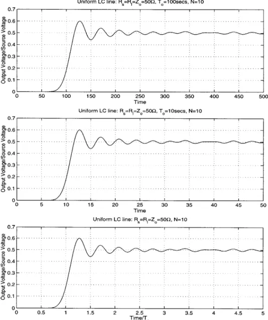
2.4.1 Scaling by T, = v LO
All other parameters held constant, varying an LC line's propagation delay results in
a scaling of the time axis. As a result normalizing the time axis by T, yields a general waveform in time. Figure 2-3 illustrates this by showing the output of a lumped LC line for two different propagation delays and then normalizing them. In all cases it is clear that changing T only results in a compression or expansion of the time axis.
Uniform LC line: R=R =Z,=50 , T =100secs, N=10 - - - -.- -.-.- --.--. . . . . . - - w- -- --- ---... -... ---....- ..- . ---...-. --. - --. . .... .. .. .. ..-. -. - --. ..-.-- .-- -.-. ..-.-. -. .- -.- .- .- ..-.-- - .. -00 50 100 150 Uniform LC 200 250 300 350 Time line: R =R Z =500, T =10secs, N=10 400 450 500 0 5 10 15 20 25 30 35 40 45 5 Time Uniform LC line: R =R-Z =50K, N=10 7 6 -- . .. . .. .-. .. .- - - -.- -.--.- -.-.- -.-. 5 -. . . .. . . . . 4 ... 3-0 0 0.5 1 1.5 2 2.5 3 3.5 4 4.5 5 Time/T
Figure 2-3: T, Scaling on the output of various 10 stage LC lines
0.7 00.6 0 0.5 50.4 ci) 0.3 0 0.2 0.1 0.7 a) 0)0.6 0 >: 0.5 o0.4 ci) 0.3 0 0.2 0.1 0. Y 0. 0. >0. 00. C/0 M' 0. 0. 0. 00. - -- - .. .- .. . . - - -- -. -.... - ... -... - ~ ~ -. ~ ~ . . .-. .-- .. ---. - --- - - -- - --- -- - -w -... -... -..-.-.-. -.-.-0
2.4.2 Scaling by Z, = L
For a normalized time axis, it can be shown that the wave behavior along a lossless LC line, depends only on the input, the number of stages and the relative impedances
along the line. Mathematically,
WaveBehavior =
f
(Input, N, Rsource RLod (2.12)ZO Zo
Figure 2-4 shows this by giving the output response of two separate, double-matched LC lines. Although the characteristic impedance of each line is different, the behavior
depends only on the the impedance relative to the source and load resistors.
Uniform LC line: Rs=R 1=Z=500, N=10 0.7 S0.6 0 aD 0.5 0 00.3 >0.2 0.1 -15 0 0 0.5 1 1.5 2 2.5 3 3. Time/T 0 Uniform LC line: R=R1=Z0=100Q, N=10 0 0.5 1 1.5 2 2.5 Time/T 5 4 4.5 5 3 3.5 4 4.5
Figure 2-4: Z, Scaling on the output of various 10 stage LC lines
- - - - . --. .. . . . . . . . . .. . . .: -- - . . . . .
.
...
--. -. -. . . . .. . . . . . .-.. . . -.. - -.-.-.--.-.--. -. .. .-. .. .-. -. .. .--. .. . .. . .-. .. . . -.. -. -. --. . . . - ... . . .. .. .-- - .-- . . . . . -. .-. . ... . . . .-. -. .. . . . . .. . . .. . . . .. . . . . ...-...-. . ..- . .. -. 0.7 (D _ 0.6 0 00.5 00.4 c0.3 0)0 > 0.2 -0.1 0 . . . .1 - - - -- ... ... - - . ... - - .. -.. .. . . . . . . . .. . . . ... . . . .. - -. . . . .. . . . .-.. -.. -.. . . . . -. . . ... . . .- . . . .. ..-. -. . .-. .. . . . . . . . . -- - - -.. .. . . . ...... ..- . ... ... ..- . ... ... ...- -- - .. ... ... ... ... ..- . ... ... ... ... ... . . 52.4.3
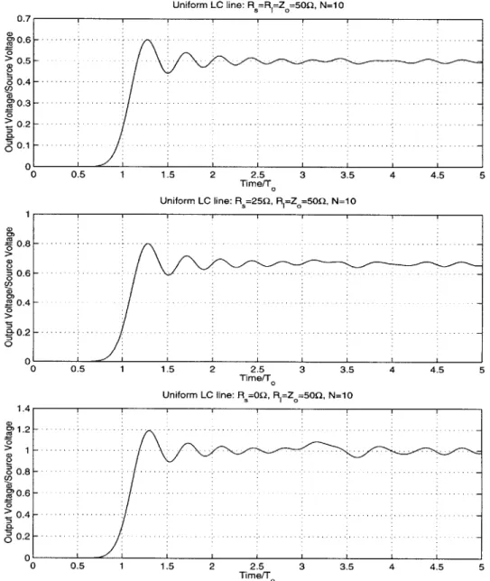
Load and Source Mismatching
In an ideal transmission line driven by a step source, matching the load to the char-acteristic impedance results in no reflections. The value of the source resistance only affects the amplitude of the output. Similar responses are exhibited by an analogous LC line. In Figure 2-5 it is seen that the response is identical (excepting the ampli-tude) until about 3T. Because the LC line is not a perfect transmission line, some
Uniform LC line: R =R =Z =500, N=10 0.7 0.6 0 >0.5 60.4 U) 0 0.3 0 0.2 0=0.1 0 1 0) 0.8 0 0.6 0 CO .0 . CL 0.4 0 1 .4 0)1 .2 0 > 1 5 0.8 a) 0)0.6 0 0.4 0.2 0. 0 0 0.5 1 1.5 2 2.5 3 3.5 4 4.5 5 Time/T Uniform LC line: R =25Q, R -Z =50!), N=10 ! .. -. . .. . .... .. .-. -. -. . . .. .. . . .. .- .-. .-.-. .-.-. .-. .-.- ..-.-. .-. .-. -- - - - -- -- - - - - --- - -a -... --- --- -.... --- -.---- .. ---.---..-0 0.5 1 1.5 2 2.5 Time/T 3.5 4 4.5 5 Uniform LC line: Rs=0M, R =Z=5092, N=10 . . . . . . .. . . .. ..I . . . . . . . . I I- - - - ---.-.-.--.-.-- a -0 0.5 1.5 2 2.5 Time/T 3 3.5 4 4.5 5
Figure 2-5: Output of a 10 stage LC line Driven by a Unit Step when Road is matched and R, is mismatched - - - -- . . . . . - --... ... -.... --.... - -..-.-.-.--. . . ..-. -. -. .. . -. . .. .-. -.-. . .. . . .. . . . . .. . . . .. . . . . .-. .-. .- . - - - - -- -- - - -q .. . . . ... "j ,
-reflections are evident after 3T,, which is approximately the time it would take the reflected wave to reach the output.
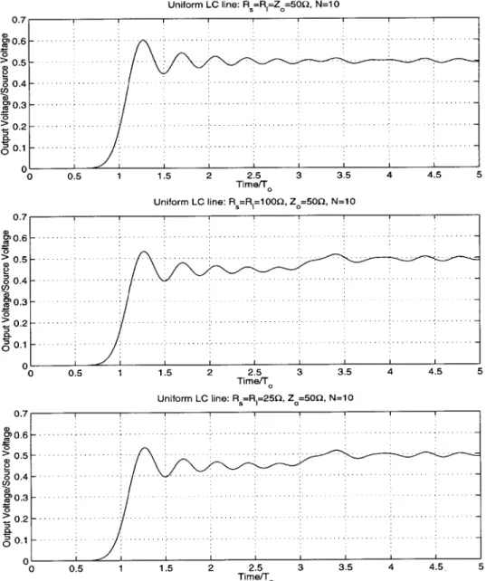
In Figure 2-6 RLoad and Rsource are mismatched to Zo by a factor of two smaller
and larger. As expected, the output behavior is the same (although the internal reflections, not seen here, are different).
0. 0. 0. 0 00. Ul) 0 0 0 0.6 0 > 0.5 60.4 0.3 0 0.2 0.1 Uniform LC line: R =R =Z =50Q, N=10 5 4q 0 0 0.5 1 1.5 2 2.5 3 3.5 4 4.5 Time/T0 00
Uniform LC line: R,=R I=1000, Z =50Q, N= 10
0 0.5 1 1.5 2 Uniform LC line: - - - .- .. . . ... .. . .. . .. --.. -.--.-.--.--. . . ... . . . . . . .. . . .. . . . ... . . . .. . . . ... .. ... ... .. ... .... .. ... .. ... .... . ... ... .. ... ... ... .. ... ... . -- - - - -- -a - . .. .- . . . . .. . . . .. . . . ... . . . .. .-. --. -. -. . .. . . -. 2.5 3 3.5 Time/T R =R =25!Q, Z =500, N=10 4 4.5 5 0 0.5 1 1.5 2 2.5 Time/T 3 3.5 4 4.5. 5
Figure 2-6: Output of a 10 stage LC line Driven by a Unit Step when Rjoad = R, = 2Z,
or .5Z0 0. 0. 0 > 0. 00. Cl) 0. MO. 0 >0. 0 0. 7 3-2 -.1 -... . . .. 0. . . . . . .. . . . L-
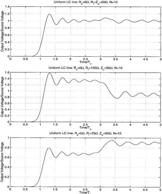
-In Figure 2-7 RLoad is mismatched to Z, by factors of two again, but Rsource has
been set to zero. The lack of a source resistance to absorb reflections is now evident in the output response after 3T,.
Uniform LC line: R,=0Q, R =Z =50, N=10 0.5 1 1.5 2 Uniform LC line: F - - - - 3 .5 - - -. - - ---. .--- .-- -. - .... -... ... ....- - ...- - - ...-- - -.. - - -- - q- -- -- - - - ---. . .. . -. . .. .- . . .. .-- . .. . .. . -. -.. . .. . - .-.. -. ---- - -.... ----... -.... ----...- ....- ... ---... 2.5 3 3.5 Time/T =0, R,=100 , Z0=500, N=10 1.5 2 2.5 Time/T 4 4.5 5 3.5 4 4.5 5 Uniform LC line: R =0Q, R 1=250, Z0=500, N=10 1 .4 - -.. . . . . .- -.2 - - -. . . . .. . .-. . . . ... . . . .- - - - --.- -. .-.-. 0 0 0.5 1 1.5 2 2.5 3 Time/T
Figure 2-7: Output of a 10 stage .5ZO but Rs = 0 3.5 4 4.5 5 1.4 1.2 -0>1 - 00.8-U) C 0.6-0 0.4 -0.2 0 0 1.6 -t 1.4 - 01.2-UD 21 -0 0.8- a0.6- 50.4- o0.2-0 -0 0.5 0 __0U 0 Cl) V 0. 0
LC line Driven by a Unit Step when Ricad = 2ZO or
I -. -. . . .. . . . . . .- -. -. -. . .. . . .. . .-.-. -- - - --a-- - --.. . . . .-- - --. .- ..- ..- .. --. -..
.
...
. -. .-.-.-. .-.--.-. -. -- -.-.-. -. -. .. . -. - -- - -- - - -.. .. .. ... .. .. ... .. ..- - - -- --..2.4.4
N-effects
The number of cells in an LC line plays an important role in the behavior of the structure. It is helpful to think of the influence of N from two viewpoints. The first is to keep the "electrical length" of the line fixed, and to subdivide the inductance and capacitance by N. This was seen earlier, and is the method by which transmission lines are approximated by lumped models. This interpretation is known as the viewpoint of increased resolution in space. The second interpretation is that increasing N lengthens the line; the inductance and capacitance per stage are kept constant and a larger N means a longer "electrical length". Because of the T scaling property, both viewpoints are related in time by a factor of N. To convert from increased resolution to greater length, one needs only to multiply the time axis by N. Figure 2-8 shows how increasing the resolution of the system affects the step response of a double-matched uniform
LC line.
Discretization Effects of a Uniform LC line: Rs=R1=Z , N=1,2,4,8 -. . . ..-. . -. . . .. . . .-. . . . . .-.--.. . . . .-. .. ..-. . ..-. .. . -. 0.7 0.6 0.5 CD CM cc 0
/
..
..
..
..
0 1 2 3 Time/To 4 5 ... ... ... ... ... 6Figure 2-8: Discretization Effects of a Double-Matched, Uniform LC line: N=1,2,4,8
-.. . .. . . -. . .- .. -. . - -.. . ..- . ... . ... . . . . . . . . .. .. . . . . . . . ... ... ... ...
As expected, the rise time of the system decreases and the delay time approaches one T as N goes up. The system also exhibits a fair amount of ringing and overshoot as N is raised. This behavior is similar to the Gibbs phenomena except that in the limit, Gibbs approaches an overshoot of approximately 9% at the discontinuity while in this case it is higher than 25%. Figure 2-9 supports this by showing the behavior of a higher N system.
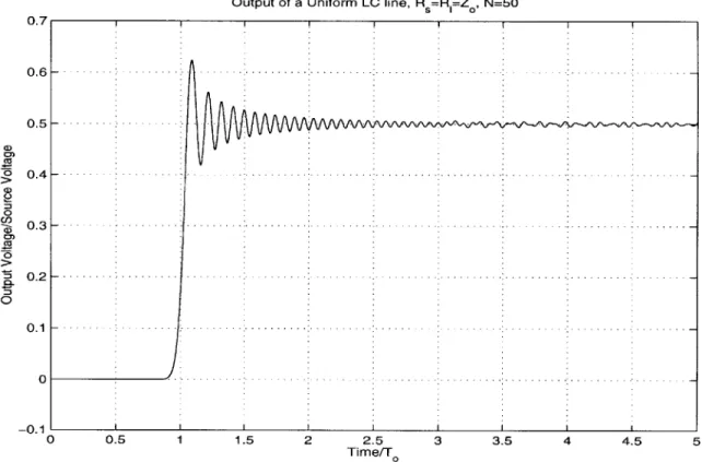
Output of a Uniform LC line, Rs=R,=Z 0, N=50
0.7 , 1 1 1 1 1 ci) 0) cci 0 ci) 0 0) - 0 .1 L ' 1 1 1 I I I 1 1 0 0.5 1 1.5 2 2.5 3 3.5 4 4.5 5 Time/T
Overshoot
Figure 2-10 depicts the overshoot trend as a function of N for up to 50 stages. The overshoot increases rapidly to about 20% for the first 10 stages and then begins to taper off, steadily increasing to overshoots greater than 25% for N=50+.
10
5
O'
C
%Overshoot of Output vs. Number of Cells (N)
0 O o o 0 0 ~ o ~ o o O o o o o ooOo o o oo6000 00 06 00 00 I I - -- -- --5 10 15 20 25 30 35 40 45 50 Number of Cells (N)
Figure 2-10: Output Overshoot of a Double-Matched, Uniform LC line vs. N 25 20 15 0 0 0 >
Rise Time
Figure 2-11 shows the influence of N on the output rise time. The time axis has been normalized by both T,, and T N to illustrate both interpretations of changing N. In the former, increased resolution, the rise time tends towards zero for large N. For the latter, lengthening the line causes the rise time to increase towards infinity with N.
10% to 90% Rise Time Normalized by T vs. Number of Cells (N) 2 1.5 E~=1 t-0.5 0 45S 0 0 0000 -I - - - -O 5 10 15 20 25 30 35 40 45 5 Number of Cells (N)
10% to 90% Rise Time Normalized by T /N vs. Number of Cells (N)
0 OQO -. . . -. ..- . . 000000 0 0 -0-- 00000 - - -5 10 15 20 25 Number of Cells (I 000000000000 -0 -0 -0 .. . . . .. . . . .. . . . 30 35 40 45 50
Figure 2-11: Output Rise Time of a Double-Matched, Uniform LC line vs. N 4 4- 3-CD CC2.5 - 2-1.5 0
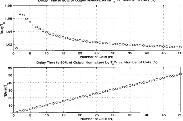
Delay
Lastly, Figure 2-12 presents the effect of N on the output delay. As expected, the delay approaches one T for higher N's, except for the case of N=1 which apparently has a delay very close to T to begin with. Similarly, lengthening the line simply results in a greater delay.
Delay Time to 50% of Output Normalized by T vs. Number of Cells (N) 1.08 1.06 0 Co 1.04 1.02 ~00 0 0 - . 000 00 0000000000000 0 5 10 15 20 25 30 35 40 45 5 Number of Cells (N)
Delay Time to 50% of Output Normalized by T /N vs. Number of Cells (N) 0
0
5 10 15 20 25
Number of Cells (Q
30 35 40 45 50
Figure 2-12: Output Delay of a Double-Matched, Uniform LC line vs. N 50 ,40 .C 30 20 10 r_ n 0 000 0 -. . -00-0 000--0000 ooo rI0~ 0 I GO
Chapter 3
Uncharged, Switched LC Lines
3.1
Introduction
This chapter introduces the uncharged, switched LC line. This structure is not a practical distributed switch because it does not properly divide the voltage across each switching element: its main purpose is to study how the inclusion of switch elements in the LC structure affects wave propagation through the line. In particular, the firing pattern of the switching elements gives a new degree of freedom for modifying the output response of the line.
3.2
Modeling Uncharged, Switched LC Lines
The LC model introduced in Chapter 2 is modified to include an ideal switch in series with the inductance L as seen in Figure 3-1. For now, the switch is specified to close at some arbitrary time, Tciose = to, and the cell is defined to be at rest at that time.
IL(t-tO)=O
A B
Tclose=tO L +
C VC(t<tO)=O
A' B'
Figure 3-1: Uncharged Switch Model
The line model, given in Figure 3-2, follows as before by cascading N of the cells in series. Once again, the line is terminated at both ends and is driven by a voltage source in order to provide a means of exciting the system. Because the entire system is at rest at time to the line is said to be "uncharged".
Rsourc A SI L(t<t0)=0 S2IL(t<tl)=0 Sn I(ts~tn)=0 la
Rsource A Si S2___S B Rload
Tclose=tO L/N + Tclose=tl L/N+ Tclose=tn L/N +
Vdc + C/N VC(tstO)=O C/N VC(t<tl)=O C/N VC(t<tn)=0
.. T
TT
..
(A' B'
Figure 3-2: Uncharged, Switched LC Line Model
3.2.1
Scaling Property
In general, the inclusion of switching elements into a linear network yields a network that is nonlinear. However, if it is permissible to model the switching elements as ideal, then the system can be thought of as piecewise LTI[6]. Because these models use ideal switches exclusively, they are also piecewise LTI. It is this attribute that preserves the properties of scaling seen in Chapter 2.
Scaling by T
By definition, an ideal switch commutates instantaneously: no time is lost before the
longer LC line that inherits its current state from the previous line. In other words, with each switch transition, a new circuit topology is formed, whose initial conditions are set by the previous topology prior to switching. As long as the switch closing times are also scaled then the system's state from transition to transition will be identical on a normalized time axis.
Scaling by Z,
Ideal switches constitute either a zero or infinite impedance, depending on their state. Consequently, the impedance from an LC cell relative to the switch impedance is also zero or infinite, regardless of the characteristic impedance of the line. Since it is only the relative impedance that matters, this property also holds.
3.3
Distributed Switch Triggering
This thesis does not attempt to study the impact of all possible firing schemes on a distributed switch; instead, one specific scheme, referred to as Fixed Inter-Switch Delay Triggering (FIDT) is investigated. FIDT is most readily compared to a se-quence of N dominoes equally spaced in distance. Tipping the first domino starts a chain reaction in which each successive domino falls at a fixed time with respect to the previous domino.
Using a FIDT scheme the closing time of a switch, Sn, can be described mathe-matically as follows,
Tcose(n) = K "(n - 1), (3.1) N
To= VLC, (3.2)
where the closing time referenced to the previous switch is equal to 1 scaled by anN arbitrary variable referred to as 'K'. It can be shown that 'K' is the inter-switch delay, ATISD, normalized by 'T . First define the inter-switch delay to be
Substituting and simplifying, KT Tciose (n + 1) - Tciose((n) = 0 (3.4) Solving for K, K - [Tclose(n + 1) - Tcose(n)] (3-5) To/N
The circuit interpretation of this relationship is shown in Figure 3-3.
S1 S2 S3 SN
A _____ B
Tclose= Tclose= Tclose= Tclose= K*O*To/N K*1*To/N K*2*To/N K*(N-1)*To/N
A' B'
Figure 3-3: Fixed Inter-Switch Delay Triggering Scheme
3.4
PSPICE Simulation
To further the understanding of how a FIDT scheme affects the response of an un-charged switch line, a simulation study was conducted using PSPICE. PSPICE's component library includes switch models (in addition to traditional passive com-ponents) which facilitated the modeling of distributed switch lines. In addition, its ability to post-process waveforms made it well suited to this study. Unfortunately, the version of PSPICE used has a component limitation that prevented the study of lines greater than 15 stages. Because of the sheer number of parameter combinations and a desire to experimentally verify simulation results, the majority of simulated lines were chosen to be five stages long. A distributed switch of N=5 is long enough to demonstrate the major effects of the lumping process, but is short enough to build hardware versions for testing.
3.4.1
Wave Propagation(K)
Of primary interest is how the K factor influences the way waves propagate through a distributed switch. In order to establish a reference, the base case is defined to be K=0, which corresponds to simultaneously triggering all of the switches. From a circuit viewpoint all of the switches are shorts at time t=0, meaning that the switched structure is identical to the lumped LC line seen in Chapter 2. Figure 3-4 shows the voltage propagation at each node for a step input into a double-matched, uncharged switch line for K=0. It is observed that the 3rd to last wave has the greatest amount of overshoot, but that the 2nd to last wave suffers the greatest sustained ringing. Also because of the lumped model approximation, the input is able to affect the output starting at t=0+, although only by an infinitesimal amount.
Wave Propagation in a Uniform Uncharged Switch: Rs=R1=Z , N=5, K=0
0) 0 Q? 0.5 a) 0 > 0.4-'a 0 z 0.3-0.2 0.1 0 '' a-0 0.5 1.5 2 2.5 3 3.5 4 4.5 5 Time/To
Figure 3-4: Voltages in a Uniform Uncharged Switch: R, = R, = Zo, N = 5, K = 0 If a K=1 is used, a noticeable effect is clearly seen on the capacitor voltages with time. Specifically, the overshoot throughout the structure has increased. In essence, the switches have provided a means of building up the energy in the preceding stages
1 ... ... ... - ----. . .. . --.. . .. . . . - - -. --.. . . . ..-. -. .. -.. . ... -. .. . ..-. . .. .
before charging up the next cell. Again, the third to last node has the greatest overshoot, and the second to last has the most sustained ringing. In addition, the switch delays have produced a "sharpening" effect on the node voltages, the rise times have decreased throughout. This improvement in rise time can be attributed to two major factors. The increased voltage driving each stage implies a larger L! and hence a faster rise time. Also, the switches prevent the source from affecting the response at each node before they are switched; this further sharpens the initial rise of each wave.
Wave Propagation in a Uniform Uncharged Switch: RS=R,=ZOI N=5, K=1
... ... ... ... ... .... ... ... . ... ... .... .... ... .... ... 0 0 0 >) 0 a) 0.1 ... .-. -.- .... -... . . .. ..I. . . . .. 1.5 2 2.5 Time/To 3 3.5 4 4.5 5
Figure 3-5: Voltages in a Uniform Uncharged Switch: R, = R= Zo, N = 5, K = 1
3.4.2
Internal Stresses
When designing an actual high voltage switch, care must be taken to insure that not only is the output response of the system well behaved, but that the internal behavior is not destructive. This raises the issue of controlled internal stress, since eventually a structure that contains real switches internally is to be built. Introducing
0 1L 0 0.5 ... ... ... ... ... ...
a systematic delay into the LC structure provides a means by which wave propagation can sum destructively within the distributed switch. However, since the uncharged, switched line does not reduce the individual switch stress correctly1, the focus here is exclusively on the voltage across each capacitor and the current through each inductor. A study of the "true" switch stress will be saved for the precharged case where it is appropriate.
Capacitor Voltages
Parametric sweeps of the peak positive and negative capacitor voltages for 0 < K < 3 were conducted. Figure 3-6 shows the plot of peak positive voltages. It is noted that the peak voltage of C5 is actually below 63% of the source voltage for K < 1. This corresponds to an overshoot at the output of less than 26%, because the final voltage is actually half of the source voltage due to the equal double-ended termination. For
Peak Positive Capacitor Voltage vs. K
e C1 1.3 C2 1C3 *C4 1.2 - E- C5 -a) 0 0) ca 0.7 0.5 1.5 K 2 2.5 3
Figure 3-6: Peak Positive Capacitor Voltage vs. K
K > 1 the stress at the internal nodes grows rapidly although the output remains bounded up to at least K=3.
Figure 3-7 provides additional insight into the behavior of the system for higher values of K. In particular, starting around K=1.4, oscillatory behavior large enough to cause the node voltages to swing negatively is seen. This phenomena begins at the second to last node, the node which typically exhibited the most sustained ringing. As K is increased, this negative transition moves down the structure towards the source end. At no time does the output exhibit a negative peak voltage for K < 3.
Peak Negative Capacitor Voltage vs. K
K
Figure 3-7: Peak Negative Capacitor Voltage vs. K
Inductor Current
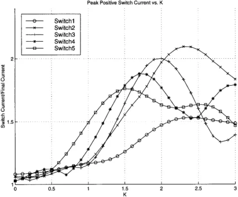
Perhaps more important in terms of the switch stress is knowledge of how the inductor current behaves throughout the line. Because the inductor is modeled in series with the switch, this is the current the switch must tolerate. Figure 3-8 shows how the peak
current of each inductor, normalized by the steady state DC current2 is influenced
by K. Here the inductors closer to the load must tolerate greater currents for K < 1. Again as K is increased beyond one l additional reflections cause ringing to increaseN quickly. Interestingly, the inductors at the extremes of the line suffer less overshoot than those within the line, presumably because they are closer to the termination resistors.
Peak Positive Inductor Current vs. K 2 .5 - - .- . -.-..-.-. .- -. - - - -- ---E L1 - - L2 -+-- L3 *- L4 -- L5 0 0 C: 0 0 0.5 1 1.5 2 2.5 3 K
Figure 3-8: Peak Positive Inductor Current vs. K
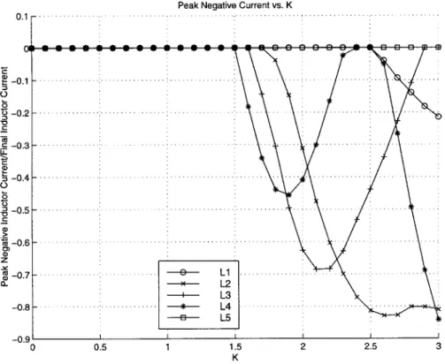
Figure 3-9 gives further evidence that operating around K's greater than one can be hazardous. In particular, around K=1.5 the currents in the inductors begin to reverse directions completely! This corroborates the phenomena seen previously with the capacitor voltages and suggests that the mode of operation in the line is changing. In a true switched line, careful attention should be paid to look out for similar behav-ior, especially since many solid state switches do not support bidirectional current!
Peak Negative Current vs. K 0 .1 . . . . .- . .. . . .-.. -.. . .. . . .-.. . .. . . . . . . .. . . .-.. -.. 0 . . . .. .. .. .... .... . ... ... .. .... . . ... ... LLL C (D . .. . . -. -- *. . a- L5 -0... ... L ... -o9 0.5 1 1.5 2 2.5 3 K
Figure 3-9: Peak Negative Current vs. K
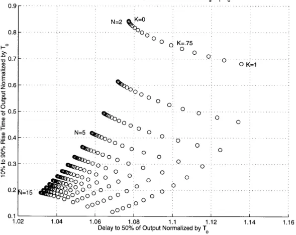
3.4.3 N Effects
The influence of the number stages in an uncharged switched line is
just
as importantas in the fixed LC line case. Unfortunately, the introduction of the K variable greatly increases the parameter space. Consequently, an exhaustive study of how N affects
the response of the line over a broad K space is difficult. To make study of this aspect feasible, K was limited to values of one and smaller. This is a reasonable constraint, since it was seen that for large K the switched line began to suffer increased internal stresses. As mentioned earlier, the data was further restricted to N< 15 due to simulation limitations. The following plots show the 10% to 90% rise time of the output versus the delay time to 50% of the output for double-matched, uniform, uncharged switched lines as functions of the implicit variables K and N.