HAL Id: tel-02324989
https://tel.archives-ouvertes.fr/tel-02324989
Submitted on 22 Oct 2019
HAL is a multi-disciplinary open access archive for the deposit and dissemination of sci-entific research documents, whether they are pub-lished or not. The documents may come from teaching and research institutions in France or abroad, or from public or private research centers.
L’archive ouverte pluridisciplinaire HAL, est destinée au dépôt et à la diffusion de documents scientifiques de niveau recherche, publiés ou non, émanant des établissements d’enseignement et de recherche français ou étrangers, des laboratoires publics ou privés.
Fabrication et caractérisation de transistor réalisée à
basse température pour l’intégration 3D séquentielle
Jessy Micout
To cite this version:
Jessy Micout. Fabrication et caractérisation de transistor réalisée à basse température pour l’intégration 3D séquentielle. Micro et nanotechnologies/Microélectronique. Université Grenoble Alpes, 2019. Français. �NNT : 2019GREAT008�. �tel-02324989�
THÈSE
Pour obtenir le grade de
DOCTEUR DE LA COMMUNAUTE UNIVERSITE
GRENOBLE ALPES
Spécialité : Nano électronique et Nano technologie
Arrêté ministériel : 25 mai 2016
Présentée par
Jessy MICOUT
Thèse dirigée par Gérard GHIBAUDO, HDR, CNRS Alpes préparée au sein des Laboratoires CEA-LETI et IMEP-LAHC dans l'École Doctorale Electronique, Electrotechnique, Automation et Traitement du Signal
Fabrication et caractérisation de
transistors réalisés à basse
température pour l’intégration
3D séquentielle
Thèse soutenue publiquement le 08/03/2019, devant le jury composé de :
M. Francis, BALESTRA
Directeur de recherche, IMEP-LAHC (Président)
M. Fuccio, CRISTIANO
Directeur de recherche, LAAS-CNRS (Rapporteur)
M. Pascal, MASSON
Directeur de recherche, Université de Nice Sophia Antipolis (Rapporteur)
Mme. Perrine, BATUDE
Ingénieur-Docteur, CEA-LETI (Co-encadrante)
M. Quentin, RAFHAY
Ingénieur-Docteur, IMEP-LAHC (Co-encadrant)
M. Gérard, GHIBAUDO
Jessy MICOUT Page 1
ACKNOWLEDGMENTS
Je viens d’éteindre mon écran d’ordinateur. Posé sur ma chaise, je regarde le bureau sur lequel j’ai travaillé pendant trois ans. Sur la gauche se tient mon co-bureau François, toujours disponible pour une anecdote surprenante ou pour un conseil des plus avisé. A ma gauche, mon téléphone de service reste silencieux. Pour autant, il aura énormément sonné, et j’avais notamment au bout du fil Nils, une personne très patiente et efficace, pour lui faire part des dernières modifications journalières des différents process flow. Il y avait aussi toutes les personnes de la salle blanche du CEA, et je me rappellerai surtout des appels (et soutiens) de Vincent, mon tuteur temporaire qui m’aura tant apporté en si peu de temps, de Jean-Michel « Jim » et de sa grande pédagogie, des conseils apportés par Benoît S., Joris et Fred sur les implantations/simulations –ô combien nécessaires-, et j’en passe.
Enfin je sors de mon bureau. En face de moi se tient le couloir qui permet de sortir de mon étage. Mais je décide, une dernière fois, de faire le tour des lieux. Sur ma gauche on peut apercevoir un couloir, avec deux bureaux sur la gauche, et un en face. Le premier bureau est celui de Benoît, avec qui les discussions sur la société actuelle et future étaient des plus plaisantes. En face de lui, sa co-bureau Yoon Ji, discrète mais des plus sympathiques. Dans le bureau adjacent, je me rappelle de la place vacante de Rémi, que j’ai bien embêté sur les différents concepts de
transistor, mais dont l’opinion Python vs MathCAD était commune. Sur sa gauche, Valérie, qui m’a tant aidé sur le suivi du FinFET. Sa gentillesse et disponibilité resteront marquées. En face d’elle, Christophe, dont je me souviens des discussions sur le passé de St & co. Dans le bureau d’en-face, je peux voir Louis, dont ses connaissances scientifiques et culturelles me laissent encore sans voix, et qui m’a bien rassuré sur l’avenir, quand il le fallait. En face de lui, Perrine, ma tutrice du CEA, dont son dynamisme et sa capacité à faire bouger des montagnes me laissent encore admiratif. A droite de ce bureau il y a Claire, un membre phare de l’équipe CoolCube, qui allie compétence scientifique et compréhension humaine avec perfection. En face d’elle, Olivier, expert en simulation, impressionnant à tout point de vue. Enfin, je retourne dans le couloir principal. Sur la gauche se tient le bureau de Maud, cheffe du labo et boule d’énergie positive facilement transmissible. Je me dirige vers l’autre allée en face de moi, et j’arrive dans le bureau de Jean-Michel et de Bernard. Les discussions et conseils – qui arrivaient souvent à point
nommé- au café de 7h et de 9h avec notamment Claude et Marie Pierre resteront dans ma mémoire, ça me servira pour sûr bien après la thèse. Sur la droite, le bureau de Sylvan, le post doc dont les conversations autour d’une bière valent le détour, ainsi que d’Yves, qui t’apprend à retourner une erreur réalisée en la solution parfaite à un problème spécifique. Juste à côté, le premier bureau des thésards, où je vois Camila– la nouvelle thésarde de Perrine – fixée sur son ordi à s’insurger contre MathCAD. «Be brave », le meilleur est devant toi. En face d’elle, Claude, le protagoniste du duo de choc avec Bernard Previtali le midi, se plaint d’Eyelit. Ils étaient en
Jessy MICOUT Page 2
quelques sortes ma bouffée d’oxygène génératrice. Et juste à côté, Lina, occupée à finir un design foireux ?. Elle et nos conversations interminables me manqueront pour sûr (surtout, ne rend pas publique le carnet de note !). « Rose et papillon », Lina. En face d’elle se tenait Paul, l’ex-technicien CoolCube et grand complice de voyage ou de saut à l’élastique. J’espère qu’il profite bien de sa vie, entre travail et parachutisme. Le bureau d'à côté est le second bureau de thésard, où il y a eu beaucoup de « turn over » dirait-t-on. Je me souviendrai de la première équipe
Mathilde, Luca, Julien et Alexandre qui m’ont accueilli en début de thèse. Et puis vint la seconde équipe, dont Daphnée, Giulia et les stagiaires Gaspard, Simon et Romane. Bonne chance pour votre fin de thèse ou votre nouveau job/étude et ce n’est que le début de la vie. Ça a été un grand plaisir d’être votre « guide spirituel »*. Et avant de prendre l’escalier je me rends aussi compte des personnes de cet étage qui m’ont aidé, tel que Zdenek, Didier, Fabrice ou encore Philipe, mais aussi et surtout Jean-Pierre. Je me souviendrai de ce mercredi après-midi, où après une conversation physique sur une possible solution technologique, il est venu me voir en me disant « Jessy, tu as raison » (un des meilleurs moments de ma thèse). Encore Merci à Tom –meilleur mercato d’hiver avant que je parte.
Je monte alors au second étage pour voir le restant du labo. L’autre équipe du midi est là, dont Laurent B, et Cyril. Un troisième bureau d’anciens thésards –Fabien et Aurore- me fait souvenir de ma première année de thèse, très bien passée grâce à eux. Enfin, sur l’autre allée, je peux voir le bureau de Laurent B., un autre membre star de CoolCube, avec qui je me suis toujours très bien entendu. En face de lui, Sylvain et ses talents de technologue et physicien dans les nano fils, qui restent toujours aussi impressionnants –pour le peu que j’ai pu suivre. A côté, le bureau où se tenait Vincent L., avec ses innombrables lots derrière lui. Promis, je te battrai un jour au badminton.
Je prends alors l’ascenseur, et je quitte enfin le bâtiment où j’ai passé tant d’heures à l’intérieur. Sur la droite, la machine à café où j’appréciais prendre le café (duh !?) avec Louise. En face de moi se tient la salle blanche, salle dans laquelle j’ai parlé à de magnifiques personnes, mais dont je ne pourrai pas tous les remercier à leur juste valeur car je suis limité par la technologique de mon époque. Sur la gauche, l’équipe des thésards fumeurs (ou pas), qui ont pu voir mon visage changer au fur et à mesure qu’une certaine deadline approchait. Sur la droite, au loin, mon autre laboratoire d’accueil, l’IMEP-LAHC. Malgré avoir vu les thésards plus au bar que dans ce laboratoire, les moments passés avec eux, un peu loin des problèmes scientifiques, étaient juste excellents. Mais c’est aussi dans ce laboratoire que se trouve mon directeur de thèse, Gérard « le Grand » Ghibaudo, dont sa réactivité a toujours été remarquable.
Mais c’est aussi dans ce laboratoire que se loge Quentin « Le loup blanc » Rafhay, mon autre tuteur de thèse. Si ma vie est une ville, il y aurait tout un quartier qui te serait dédié. Merci encore pour tout. Simplement.
Enfin, je quitte le CEA, et je rends mon badge à l’entrée. Et devant la montagne, je pense à ceux qui m’ont épaulé durant ces trois années, qui m’ont surtout supporté le vendredi soir au bar. C’était un moment charnière dans ma vie, et ils ont contribué à grandement l’améliorer. Je
Jessy MICOUT Page 3
remercie donc le groupe « Lundi GOT » pour tout ce qu’ils m’ont apporté, et plus
particulièrement Esther, Fabien et Minidoux, la première pour son appartement au moment de la rédaction, le second pour les soirées jeux (Mushu restera dans la légende), et le troisième parce qu’il le vaut bien. Enfin, je remercie ma famille et mes amis de toujours, « la communauté », qui m’ont supporté et tellement apporté bien avant, et le feront encore bien après. 200 pages ne seraient pas assez pour vous remercier.
Enfin, et un peu plus loin dans le temps, je remercie les membres du jury, Francis Balestra, Fuccio Cristiano et Pascal Masson pour avoir accepté de relire cette thèse et pour leurs remarques pertinentes.
*Titre auto proclamé
Jessy MICOUT Page i
CONTENTS
Acknowledgments ... 1 Contents ... i List of figures ... iv List of tables ... x 1. Technological context ... 1 1.1 3D integration ... 2 1.2 MOSFET transistor ... 51.3 Challenge for the junction formation ... 8
1.3.1 Profile influence on electrical performance ... 8
1.3.2 Extension Last/Gate First Integration process at high temperature ... 10
1.3.3 Gate First/Gate Last and Xlast/Xfirst integration schemes... 12
1.4 Goal of this work ... 14
2. Low-Temperature Extension-Last FDSOI integration ... 15
2.1 Background ... 16
2.1.1 Control of the amorphization thickness ... 20
2.1.2 SPER rate dependency ... 21
2.1.3 EOR-defects influence on electrical performance ... 27
2.2 Analysis on Extension Last integration ... 34
2.2.1 Review of previous electrical results ... 34
2.2.2 Raccess improvement ... 38
2.2.3 DIBL optimization ... 52
3. Low-Temperature Extension-First FDSOI integration ... 61
Jessy MICOUT Page ii
3.1.1 Process Of Reference process flow of a 14 nm FDSOI ... 62
3.1.2 Electricals results ... 66
3.1.3 Raccess optimizations ... 68
3.2 Extension First without liner ... 75
3.2.1 Advantage to implant through bare silicon ... 75
3.2.2 Integration proposition ... 79
3.3 EOT improvement... 83
3.3.1 Electrical measurements ... 83
4. Low-Temperature FinFET integration ... 95
4.1 FinFET introduction ... 97
4.2 Finfet junction schemes ... 98
4.2.1 Defect-crystalline integrity ... 99
4.2.2 Angle restriction and conformal doping ... 101
4.2.3 Bending Fin ... 103
4.2.4 Embedded In situ doped raised source drain epitaxy ... 104
4.2.5 Description of the FinFET process flow ... 107
4.3 Proposition for Low Temperature devices ... 109
4.3.1 Horizontal Seed configuration ... 111
4.3.2 Central Seed configuration ... 112
4.3.3 Lateral seed configuration ... 113
4.3.4 The Double SPER configuration ... 114
4.4 Fabrication and Electrical characterization ... 122
4.4.1 Process flow modification ... 122
4.4.2 Electrical results ... 126
4.4.3 Non-recrystallization default ... 132
4.4.4 Straggle and EOR density diminution... 134
Jessy MICOUT Page iii
4.5 Perspective on potential integration schemes ... 141
4.5.1 Summary of integration schemes ... 152
5. Conclusion ... 157
Bibliography ... 161
Jessy MICOUT Page iv
LIST OF FIGURES
Figure 1.1: Transistor cost and lithography tool cost versus years, from [2] ... 2
Figure 1.2: Bulk, FDSOI and FinFET architectures ... 3
Figure 1.3: Description of 3D integration process flow, in parallel integration (a) or sequential integration (b) ... 4
Figure 1.4: Illustration of the trade-off for the 3D sequential integration ... 5
Figure 1.5: nMOS transistor scheme in on state and Id-Vg characteristics ... 6
Figure 1.6: Illustration of the different components of the total resistance ... 8
Figure 1.7: Schematic illustration of the junction profile influence on the Id-Vg characteristics ... 9
Figure 1.8: Standard process flow for 28 nm FDSOI technology with gate first/Extension Last integration 11 Figure 1.9: Main differences between Gate First/Gate Last and Extension First/Extension Last integration scheme ... 13
Figure 1.10: Transistor performance versus transistor cost according to the considered integrations schemes and the architectures used in this thesis ... 13
Figure 2.1: Ion implantation and consequences on lattice crystal... 16
Figure 2.2: Illustration of the SPER process ... 17
Figure 2.3: TEM cross section picture of an as-implanted boron-doped sample and the electrical doping concentration measured by ECV, after a SPER activation at 600 °C/2 min (from [9])... 18
Figure 2.4: KMC simulations of the amorphous thickness as a function of the dose rate ... 21
Figure 2.5: Atomistic configurations for (100), (011) and (111) crystalline plane, from [18] ... 22
Figure 2.6: Schematic representation of normal and twin configuration from [31], and TEM cross section picture evidencing stacking fault ... 23
Figure 2.7: Schematic illustration of crystalline orientations for <110> and <100> -oriented channel ... 24
Figure 2.8: SPER rate as a function of the temperature and the crystalline orientation [30], and the temperature and doping specie for the <100> crystalline orientation [24] ... 26
Figure 2.9: Illustration of the EOR defects formation ... 28
Jessy MICOUT Page v
Figure 2.11: Summary of the expected degradation on Id-Vg curves due to EOR effects ... 30
Figure 2.12: Illustration of the cut-off and sinking effect, from [37] ... 31
Figure 2.13: Sheet resistance measurements as a function of the annealing duration, with different location of the EOR, from [37] ... 32
Figure 2.14: Recommendation for carbon profile to limit both the TED effect and the BIC formation ... 33
Figure 2.15: Process flow for HT and LT devices ... 35
Figure 2.16: Ion-Ioff and Ron -DIBL trade-off for p&n MOS devices. ... 37
Figure 2.17: Id-Vg and electrical schemes of 500 °C- and 600 °C- activated devices, with an analytical fitting. ... 38
Figure 2.18: a) TEM observation of a 500 °C-activated device, b) Ion-Ioff performance of the observed device ... 39
Figure 2.19: Electrical simulation by taking into account the precise dose rate of the amorphization profile in .a) and the time-annealing evolution at 500 °C in .b), and TEM cross section picture in c). ... 40
Figure 2.20: Ion-Ioff trade-off before and after a post back end supplementary annealing (500 °C/10 min) 41 Figure 2.21: 3D view of the recrystallization mechanism with amorphization profile shown in Figure 2.19.a) ... 42
Figure 2.22: TEM cross section picture of 600 °C-activated nMOS (.a), 500 °C-activated pMOS (.b) and 500 °C-activated nMOS (.c)... 43
Figure 2.23: Time-annealing evolution of 600 °C-activated nMOS (.a), 500 °C-activated pMOS (.b) and 500 °C-activated nMOS (.c)... 44
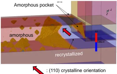
Figure 2.24: Expected recrystallization mechanism for two seed configurations ... 45
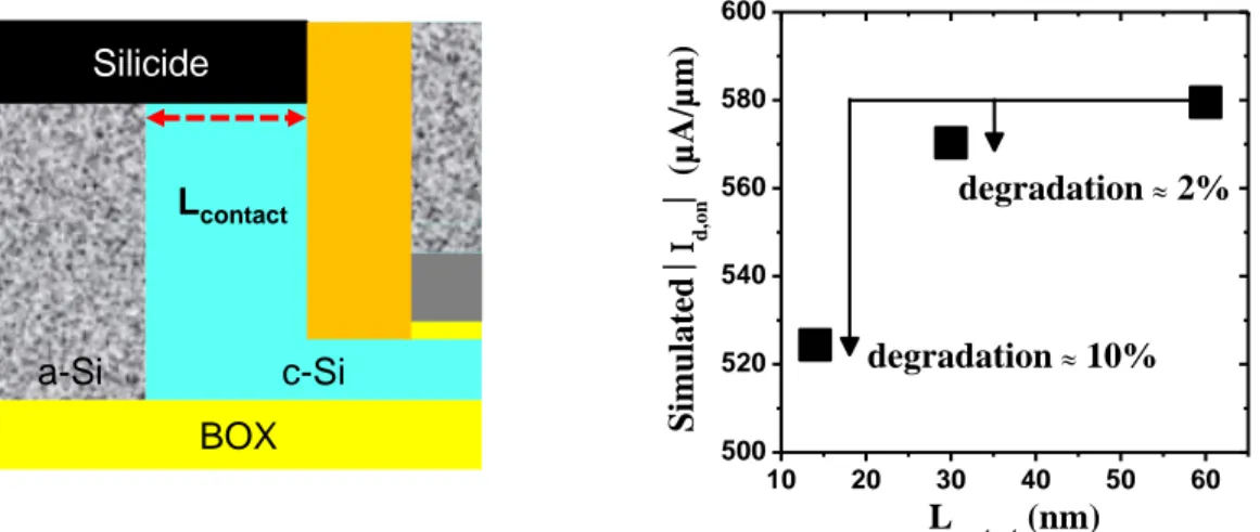
Figure 2.25: 28 nm electrical simulation for nMOS splits, evidencing the negligible influence of the Silicide/c-Si interface length (Lcontact) above 30 nm ... 46
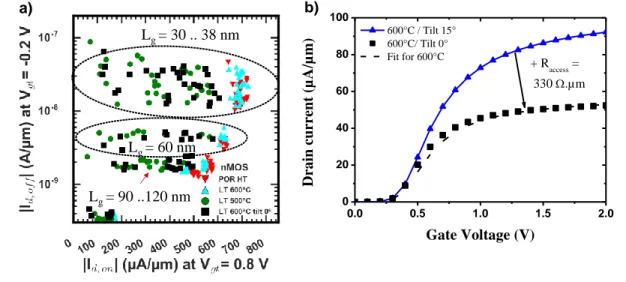
Figure 2.26: KMC simulations of the a/c front with <110>-and <100> oriented channel, for 600C°C-activated nMOS. ... 48
Figure 2.27: Ion Ioff and Id-Vg curve with 600 °C/tilt 0° split ... 49
Figure 2.28: time annealing evolution for 600 °C activated nMOS devices, with or without tilt ... 49
Figure 2.29: KMC simulation of oxygen and nitrogen recoil ... 51
Figure 2.30: DIBL as function of Lg for HT and LT split ... 53
Figure 2.31: Process simulations of the boron chemical-concentration profile, a) as implanted and b) after a 630 °C/2 h annealing. ... 54
Jessy MICOUT Page vi
Figure 2.32: Boron solubility as a function of the temperature from [54]... 56
Figure 2.33: Process simulations as implanted of the boron chemical-concentration profile, with a reduction of the boron concentration in the channel ... 57
Figure 3.1: Process flow of HT POR devices for a 14 nm technology ... 63
Figure 3.2: Diverging steps in the process flow of High-Temperature and Low-Temperature devices ... 65
Figure 3.3: Ion-Ioff trade-off from [57] ... 67
Figure 3.4: Raccess for low temperature splits from [57] ... 68
Figure 3.5: Illustration of the morphological result, and the interpretation for electrical device ... 69
Figure 3.6: (a) Measured Rsheet and (b) calculated Rsheet as a function of the activation level for low temperature splits from [1] ... 70
Figure 3.7: EDX and TEM of No PAI sample on full sheet after 600 °C/ 2 min annealing ... 71
Figure 3.8: SIMS of the as-implanted n-type samples ... 71
Figure 3.9: (a) LT and HT device configuration and (b) Rspa as a function of the offset spacer thickness . 73 Figure 3.10: Ion versus the doping concentration into the RSD ... 74
Figure 3.11: Structures used for to study the nitrogen and oxygen recoil into dopant deactivation ... 76
Figure 3.12: Dopant profiles and TEM cross section pictures after implantation (through bare silicon splits) ... 77
Figure 3.13: Rsheet results of p and n type, though nitride, oxide and bare silicon ... 78
Figure 3.14: Main step modification into the Extension First integration scheme to implant without nitrogen recoil ... 79
Figure 3.15: Tsi consumption according the etching recipe ... 80
Figure 3.16: CD measurements during the process flow ... 81
Figure 3.17: Main steps of the X1st/Gate Last integration scheme ... 82
Figure 3.18: C-V measurements and extracted EOT for LT and HT devices ... 84
Figure 3.19: Ig-Vg for LT splits according to three gate lengths ... 85
Figure 3.20: Normalized Ig,lin vs Lg for both methods ... 88
Figure 3.21: Comparison between simulated and experimental gate current for short and long gate lengths ... 90
Jessy MICOUT Page vii
Figure 3.23: Illustration of the oxygen-ingress phenomenon ... 92
Figure 4.1: Planar and Fin FETs on SOI architecture. ... 97
Figure 4.2: Implantation-angle definition for this work ... 99
Figure 4.3: TEM picture from [5]. Due to the surface proximity, new recrystallization fronts appear, and can cause defect formation. ... 100
Figure 4.4: Angle restriction for tilted implantation for a) unipolar and b) N|P transition region (SRAM configuration) ... 101
Figure 4.5: Illustration of the single-sided implantation ... 102
Figure 4.6: Hard Mask utilization to improve the angle restriction ... 103
Figure 4.7: Main steps of a FinFET flow with embedded in situ doped raised source drain epitaxy ... 104
Figure 4.8: Main steps of e-RSD with for thermal-budget devices ... 105
Figure 4.9: TEM cross section pictures of HT e-RSD FinFET with or without oxidation/desoxidation cycles ... 106
Figure 4.10: Raccess and hole mobility with and without oxidation/desoxidation cycles ... 107
Figure 4.11: Mains steps of the FinFET process flow ... 108
Figure 4.12: Structure used for simulations ... 110
Figure 4.13: TEM pictures of the fin-width cross section after two amorphizing implantations ... 111
Figure 4.14: Ron-DIBL trade-off for the horizontal-seed configuration, for different seed thicknesses ... 112
Figure 4.15: Ron-DIBL trade-off for the central-seed configuration, for different amorphization thicknesses ... 113
Figure 4.16: Ron-DIBL trade-off for the lateral-seed configuration, for different seed thicknesses ... 114
Figure 4.17: Illustration of the DSPER process ... 115
Figure 4.18: Zoom of the cross section of the fin width after the first amorphizing implantation ... 116
Figure 4.19: TEM picture of the fin-width cross section of a 35 nm-thick fin after the DSPER process ... 117
Figure 4.20: TEM picture of the fin-width cross section of a 16 nm-thick fin after the DSPER process ... 118
Figure 4.21: Variation of the measured fin width after the HF clean ... 118
Figure 4.22: Illustration of the etch-stop layer consumption, after the gate patterning, and its consequence on the process flow ... 119 Figure 4.23: Ron-DIBL trade-off for non-doped zone surrounding the fin, for different seed thicknesses . 120
Jessy MICOUT Page viii
Figure 4.24: Relative Ron-DIBL trade-off for different non-recrystallized thicknesses at the top fin ... 122
Figure 4.25: Process flow of High-Temperature and Low-Temperature devices ... 123
Figure 4.26: Diagram of the a/c interface depth for different implantation conditions ... 124
Figure 4.27: Tilted SEM pictures of FinFET devices with or without implantation prior to the epitaxy ... 125
Figure 4.28: TEM pictures at the length and width cross section of Low temperature FinFETs ... 126
Figure 4.29: Ion-Ioff trade-off of HT and LT FinFET... 127
Figure 4.30: Simulated and experimental amorphization depth for ‘Tamo = 6 nm’ splits ... 128
Figure 4.31: Ion and Ioff values plotted as a function of the fin widths ... 129
Figure 4.32: Id-Vg curves, Vt,sat, DIBL and SS vs Lg at for the ‘Tamo = 6 nm’ split. ... 130
Figure 4.33: Ion Ioff performance benchmark of FinFET devices, built on silicon channel with embedded in situ doped raised source drain. ... 131
Figure 4.34: Illustration of two possible recrystallization defaults ... 133
Figure 4.35: Ron-W for LT ‘Tamo = 6 nm’ split and HT POR ... 134
Figure 4.36: Ron-DIBL for ‘Tamo = 6 nm’ and ‘Tamo = 12 nm’ LT splits ... 135
Figure 4.37: Dopant profile simulation for ‘Tamo = 12’ and ‘Tamo = 6’ nm splits, as implanted the final profile after an 630 °C/2 h annealing ... 136
Figure 4.38: Id,min vs Lg for Lg=60 nm and for low temperature splits ... 137
Figure 4.39: Evolution of the TED and straggle effects with scaling ... 138
Figure 4.40: Process flow differentiation for low temperature devices with or without recess, and ellipsometry measurements ... 139
Figure 4.41: Relative mobility for HT POR, LT split with or without recess ... 140
Figure 4.42: Main steps of the process modification to use the S-SPER ... 142
Figure 4.43: Ron comparison between a fully activated fin and the S-SPER process ... 143
Figure 4.44: Cross sections following the fin width and gate length direction of FinFET after gate formation, with the channel etching step ... 144
Figure 4.45: Cross sections following the fin width direction of FinFET after the gate formation, with the targeted channel etching, and with an over etching case ... 145
Jessy MICOUT Page ix
Figure 4.47: Illustration of the consequence of changing the channel orientation on the recrystallization
mechanism ... 148
Figure 4.48: Illustration of a twisted and non-twisted implantation ... 149
Figure 4.49: Main steps of the non-twisted SPER... 150
Figure 4.50: Fin-width cross section after the recess ... 151
Jessy MICOUT Page x
LIST OF TABLES
Table 1: First-order extrapolation of the SPER rate (nm/min) as function of temperature, dopant
concentration and crystalline orientation ... 26
Table 2: Split table details for low temperature splits ... 36
Table 3: Temperature/annealing couple and the estimated Lcontact ... 47
Table 4: Split details for p and n MOS devices ... 66
Table 4.1: Implantation split description ... 124
Table 4.2: Minimal SiN thickness according two implantations and node configurations ... 147
Jessy micout - Fabrication and characterization of low temperature MOSFETs for 3D integration Page 1
1. TECHNOLOGICAL CONTEXT
Contents
1. Technological context ... 1 1.1 3D integration ... 2 1.2 MOSFET transistor ... 51.3 Challenge for the junction formation ... 8
1.3.1 Profile influence on electrical performance ... 8
1.3.2 Extension Last/Gate First Integration process at high temperature ... 10
1.3.3 Gate First/Gate Last and Xlast/Xfirst integration schemes... 12
Jessy micout - Fabrication and characterization of low temperature MOSFETs for 3D integration Page 2
1.1 3D INTEGRATION
For 50 years, the semiconductor market has followed the Moore law, which consists in doubling the transistor density every 18 months. Since then, industries and laboratories have followed this empirical law, as well-described by Intel in [1]: “Performance […] and cost are two key drivers of technological development. As more transistors fit into smaller spaces, processing power increased and energy efficiency improved, all at a lower cost for the end user. This development not only enhanced existing industries and increased productivity, but it has spawned whole new industries empowered by cheap and powerful computing”. Such an evolution has the consequence that, today, microelectronic is everywhere: from computer to internet of things, from automobile to spacecraft.
Manufacturing Metal Oxide Semiconductor Field Effect Transistors (MOSFETs) has thus been required in the past decades to reduce its physical dimensions in order to increase the device performance and simultaneously reduce its cost. Device dimensions are however approaching the physical limits of miniaturization, while tool cost are increasing, as underlined in Figure 1.1, which describes transistor and lithography tool costs as a function of the years.
Figure 1.1: Transistor cost and lithography tool cost versus years, from [2]
Jessy micout - Fabrication and characterization of low temperature MOSFETs for 3D integration Page 3 Merely reducing the transistor dimensions becomes more and more challenging. Besides, the scaling has also led to increase the parasitic phenomena, such as short channel effects (SCE). These effects are due to the loss of the electrostatic control by the gate on the channel. One way to overcome this issue is to reduce the active zone width, while its thickness is simultaneously increased in order to maximize the drive current of such devices. The active zone is hence called fin in reference to its shape. Another alternative is to reduce the space-charge zone by introducing a Buried Oxide (BOX), allowing to fully deplete the region. Devices built in the first (respectively second) configuration are called FinFETs (FDSOIs). The geometry difference between bulk, FDSOI and FinFET architectures is shown in Figure 1.2 (the spacers and epitaxial regrowth are not represented for the sake of understanding).
Figure 1.2: Bulk, FDSOI and FinFET architectures
It can be seen that contrary to FDSOI devices, FinFETs are inherently 3D, with the gate surrounding the channel, while the gate is only 2D in a FDSOI device. Thanks to an active zone both narrower and thicker, the charge in the channel for FinFET is controlled by the gate at the top and at the side, which maintains a suitable electrostatic coupling. Better electrostatic control is achieved thanks to the BOX for FDSOI. In this thesis, transistors will be manufactured for digital
Si Substrate Gate W FinFET architecture BOX Gate FDSOI architecture W H channel L sidewall Si substrate Gate Bulk architecture W L Si substrate Si H L Top surface
Jessy micout - Fabrication and characterization of low temperature MOSFETs for 3D integration Page 4 applications, according to the FDSOI architecture in chapter 2 and 3, and to the FinFET on SOI architecture in chapter 4.
In order to keep increasing density of integrated circuit, an alternative that is additionally compatible with these architectures is offered by the 3D integration scheme. This technique consists in stacking different transistor levels, one on the top of the other [3]. Two integration types might be distinguished. The first one is the parallel integration, where different chips are processed independently, then stacked vertically and connected afterward. The second one is the sequential integration, where transistor layers are processed sequentially and the stacked layers can be connected at the transistor scale. These two types of 3D integration are illustrated in Figure 1.3.
Figure 1.3: Description of 3D integration process flow, in parallel integration (a) or sequential integration (b)
While the manufacturing process with the parallel integration is relatively simpler, a much higher alignment accuracy is reached with the sequential one [4],[5]. This integration is an active field in the CEA-LETI. One of the main challenge of such an integration is to be able to process a high performance transistor at the top tier with a low thermal budget in order to preserve the transistor at the bottom from any degradation. As illustrated in Figure 1.4, the standard thermal budget to manufacture a transistor is indeed superior to 1000 °C, while the thermal stability of a
Bottom MOSFET process Top active formation Top MOSFET process 3D contact formation oxyde
a) Parallel integration b) Sequential integration
Bottom and top MOSFET process (separately) Stacking and contact formation
Jessy micout - Fabrication and characterization of low temperature MOSFETs for 3D integration Page 5 manufacturing MOSFET is insured at 400 °C, which corresponds to the standard thermal budget of the Back End Of Line.
Figure 1.4: Illustration of the trade-off for the 3D sequential integration
To preserve the bottom transistor, the top one should hence be manufactured at low thermal budget, below 500 °C. One of the main challenge consists in changing the dopant activation methodology that is commonly performed with a high thermal budget (>1000 °C). The technological option chosen at CEA-LETI and for this work is to form the junction of top transistors by Solid Phase Epitaxial Regrowth (SPER), allowing to reduce the activation anneal at temperatures that are compatible with 3D sequential integration. This work mainly focuses on the dopant activation with such a process in order to manufacture low temperature transistor. The SPER process will be explained in section 2.1.
1.2 MOSFET TRANSISTOR
In this section, a brief presentation of the structure and the basic principles of a MOSFET transistor are presented. For more details, the reader can refers to [6], [7].
The MOSFET is a transistor used for switching electronic signals and is usually composed of three layers. At first, a semiconductor substrate, which enables the current to flow between two regions, called source and drain (S&D). The current can flow thanks to a field effect via the polarization of a layer formed by a metal (gate) through a thin layer of dielectric material (gate
1100°C
400°C
500 °C
Thermal budget
Jessy micout - Fabrication and characterization of low temperature MOSFETs for 3D integration Page 6 oxide). The region below the gate is named channel. If the source and drain regions are doped with n-type impurities (phosphorus for this thesis), electrons are the majority charge carriers and the device is thus called nMOS. The device is called pMOS in the case of p-type impurities (boron in this thesis), where holes are the majority charge carriers. Figure 1.5.a) illustrates the nMOS transistor scheme in on state, with the region previously mentioned.
Figure 1.5: nMOS transistor scheme in on state and Id-Vg characteristics
When the gate voltage (Vg) is positive and above a specific voltage called threshold voltage (Vt), device is in strong inversion mode. An electron layer is formed below the gate stack, allowing the conduction between the source and the drain. The drain current characteristic (Id) as a function of Vg is illustrated in Figure 1.5.b). For Vg<Vt, the transistor is not conductive (off state) since the inversion channel is not formed. Parasitic effects can however lead to a conduction. For 0<Vg<Vt (weak inversion mode), the flowing current is defined as sub threshold current. In Figure 1.5.b) two different curves are shown, that depends on the drain voltage (Vd) values. At low Vd, transistors are in the linear mode, while at high Vd they are in saturation mode. Some figures of merits used during this thesis are also shown such as the on-state current (Ion), off-state current (Ioff), the minimum drain current (Id, min). The linear threshold voltage Vt, lin and saturation one Vt, sat are not equal in Figure 1.5.b). This is due to the Drain Induced Barrier Lowering (DIBL), which is one of
Vg Id source Drain Gate Vg Vd Id Channel Substrate Ion Ioff Id,min
High Vd Vd,sat Low Vd Vd,lin
DIBL
a) b)
Vt,lin
Jessy micout - Fabrication and characterization of low temperature MOSFETs for 3D integration Page 7 the SCE component. Besides, the sub threshold Swing (SS), which should be close to 60 mV/decade, might also be degraded.
In Figure 1.5.a) the source and drain are additionally considered as perfectly conducting. As the current flows through the contact lines and the source to the drain, the voltage can however drop due to the material resistivity (the silicon and metal contact). This supplementary and parasitic resistance is called access resistance. In a long channel device, the access resistances are negligible compared to the channel one. In a short channel device, these two resistances become however comparable [2]. The total transistor resistance Ron (also referred as Rtot) is then defined as:
𝑅𝑜𝑛 = 𝑉𝑑,𝑙𝑖𝑛
𝐼𝑑,𝑙𝑖𝑛 = 𝑅𝑐ℎ𝑎𝑛𝑛𝑒𝑙+ 𝑅𝑎𝑐𝑐𝑒𝑠𝑠
(1)
In this work, the access resistances will be decomposed as the sum of three components:
𝑅𝑎𝑐𝑐𝑒𝑠𝑠 = 𝑅𝑐𝑜+ 𝑅𝑒𝑝𝑖+ 𝑅𝑠𝑝𝑎 (2)
Each component of the access resistance correspond to a specific area at the source and drain regions. Rco corresponds to the contact resistance between the contacts and the doped region, Repi to the doped region and Rspa is the resistance corresponding to the zone below the offset spacer. The different contributions to the total resistance Ron are illustrated in Figure 1.6.
Jessy micout - Fabrication and characterization of low temperature MOSFETs for 3D integration Page 8 Figure 1.6: Illustration of the different components of the total resistance
In the past decades the device performance (Ion/Ioff ratio) was mainly limited by the mobility, which describes the ability of the carrier charge (hole or electron) to move through a solid according to a specific electric field. Mobility boosters, such as strain effects, were thus the main lever to improve performance. Today, the significant current degradation is due to too-high access resistance [8]. This thesis will be thus focused on this parameter, plus the non-conventional dopant activation in order to manufacture low-temperature transistor.
1.3 CHALLENGE FOR THE JUNCTION
FORMATION
The influence of the concentration profile of the charge carriers on electrical performance will be at first described, to underline the importance to position the junction profile. The standard junction formation will be secondly explained because manufacturing low-temperature transistor directly inherits from the high-temperature process flow. Four integration schemes (Extension First/Extension Last, Gate First First/Gate Last) involved in this thesis will be then described. The benefits and drawbacks related to each option will be finally presented.
1.3.1 Profile influence on electrical performance
SiRch
Rspa
Repi
Jessy micout - Fabrication and characterization of low temperature MOSFETs for 3D integration Page 9 Junctions that were originally defined in microelectronics corresponds to the interface between p-type and n-type regions. In this work, junctions represents the limit between the source (or the drain) and the channel, which is undoped in FDSOI and FinFET devices. Positioning junctions is generally defined by using the iso-concentration profile position of charge carriers. While a high doping concentration (above 1×10²⁰ at/cm3) in the Source and Drain is compulsory to lower the access resistance, the dopant concentration in the channel should be below 1×10¹⁹ at/cm3 to avoid DIBL degradation [9]. While an ideal junction for digital application is sketched in Figure 1.7.a), in Figure 1.7.b) is represented an underlapped with a small abruptness one. Figure 1.7.c) drafts the corresponding Id-Vg curves.
Figure 1.7: Schematic illustration of the junction profile influence on the Id-Vg characteristics
In Figure 1.7.a), dopants are perfectly placed under the first spacer, with a high activation level, above 1×10²⁰ at/cm3. The junction is additionally abrupt, as highlighted by the iso-concentration at 1×10¹⁹ at/cm3 very close to the high activation area. On the contrary, in Figure 1.7.b), the high activation level is located at the edge of the first spacer while the iso-concentration at 1×10¹⁹ at/cm3 is situated in the channel, which highlights a smooth junction profile in the doping concentration profile. Figure 1.7.c) summarizes the influence of the junction formation on the electrical performance of the device. In the second case, the drive-in current decreases due to a too
SI SI
a) Ideal junction b) Underlap and smooth junction c)
Vg
Id
c-Si, doping concentration > 1.1020at/cm3
Iso-concentration at 1.1019at/cm3
Ideal junction
Underlap and smooth junction
Jessy micout - Fabrication and characterization of low temperature MOSFETs for 3D integration Page 10 small activation level under the spacer. But, at the same time, because dopants with concentration above 1×10¹⁹ at/cm3 are located under the channel, the electrostatic control is not maintained, and the off-state current, the DIBL and the sub threshold swing (SS) increase. Positioning the junction is thus a key challenge to address high performances.
1.3.2 Extension Last/Gate First Integration process at high
temperature
The main steps of the High Temperature Process Of Reference (HT POR) are described in Figure 1.8 with a Gate First/Extension Last integration scheme. In that case, a 28 nm FDSOI architecture is used.
Jessy micout - Fabrication and characterization of low temperature MOSFETs for 3D integration Page 11 Figure 1.8: Standard process flow for 28 nm FDSOI technology with gate first/Extension Last integration
FDSOI devices are fabricated on a 7 nm-thick Si channel on a 25 nm Buried Oxide. The gate stack is at first deposited then etched (Gate First integration), and is composed of an HfO2, a TiN, and a Poly Si stack (Figure 1.8.a). SiN is then deposited and etched in order to form the offset spacer (Figure 1.8.b). Raised Source Drain (RSD) epitaxy is performed (Figure 1.8.c). A Lightly Doped Source/Drain (LDD) implantation is carried out (Figure 1.8.d) after the offset spacer formation to form junctions, followed by the second spacer formation (Figure 1.8.e) and a Heavily Doped source/Drain (HDD) implantation (Figure 1.8.f). Because the implantations are carried out after the epitaxy, this integration scheme is called Extension Last. A drive-in annealing is then performed in order to activate dopants and to place them below the offset spacer by diffusion
SI Si Si BOX
TiN
HfO
2Poly-Si
SiN
NiP
tSi
a) Gate Patterning
d) LDD Implantation
g) Drive-in annealing
b) Offset spacer formation
c) RSD epitaxy
e) Spacer2 formation
f) HDD implantation
Jessy micout - Fabrication and characterization of low temperature MOSFETs for 3D integration Page 12 (Figure 1.8.g). NiPtSi salicidation process is performed in order to lower the contact resistance (Figure 1.8.h). Depending on the application, several metal levels can be built in order to connect the transistors with each other and to create the electrical circuits (Figure 1.8.i).
In order to manufacture low-temperature transistor, the drive-in annealing at 1050 °C should thus be suppressed. The first consequence is that no dopant will be placed under the offset spacer, which will hence degrade the access resistances. Also, the dopant activation at 500 °C will lead to a low level activation, which will increase the access resistance. Different integration schemes are therefore proposed in order to form the junctions, which will be investigated during this thesis.
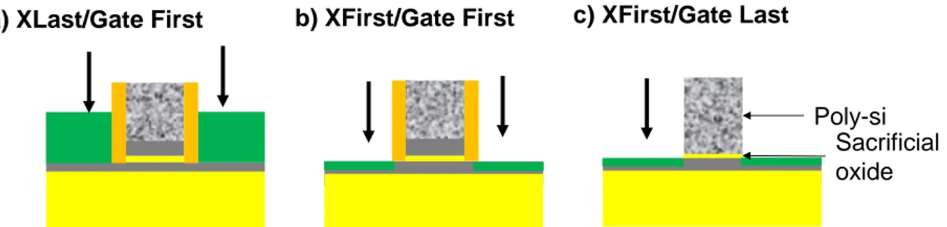
1.3.3 Gate First/Gate Last and Xlast/Xfirst integration schemes
In the previous process flow, the implantations have been performed after the epitaxy. Without the annealing, no diffusion should occur, which results in a degradation of the access resistance. Implantation condition might be tuned to place dopant below the offset spacer. But a higher dose and energy might lead to place dopant below the gate. Besides, the junction shape depends on the epitaxy thickness and shape variation. To overcome these issues, implantations might be performed before the epitaxy, and such an integration scheme is called Extension First. This will allow to dope under the offset spacer. However, when the gate is deposited and patterned before the junction formation, an offset spacer is still compulsory to avoid a gate stack degradation. For low temperature fabrication, the junction might still be misaligned with the gate stack. An additional solution is thus to deposit the gate stack after the S&D formation. For low-temperature fabrication, this might enable a better junction alignment, but at a higher device cost. The main differences in the process between the Gate Last/Gate First and Extension Last/Extension First integration schemes are summarized in Figure 1.9.
Jessy micout - Fabrication and characterization of low temperature MOSFETs for 3D integration Page 13 Figure 1.9: Main differences between Gate First/Gate Last and Extension First/Extension Last integration
scheme
Through these process flows, it can be concluded that a Gate Last/Extension First integration scheme would result in an increase of both the device performance and the device cost due to additional steps, in comparison to a Gate First/Extension Last one. In this thesis, three integrations will be investigated, and summarized in Figure 1.10, which illustrates the transistor performance versus the transistor cost according to the considered integration schemes.
Figure 1.10: Transistor performance versus transistor cost according to the considered integrations schemes and the architectures used in this thesis
a) XLast/Gate First b) XFirst/Gate First c) XFirst/Gate Last
Poly-si Sacrificial oxide T ran sistor cost Transistor performance FDSOI, Gate First, Extension Last FDSOI, Gate First, Extension First FinFET Gate Last, Extension First Chapter 1 Chapter 2 Chapter 3
Jessy micout - Fabrication and characterization of low temperature MOSFETs for 3D integration Page 14
1.4 GOAL OF THIS WORK
The aim of this thesis is to manufacture and to characterize transistors with low-temperature dopant activation, in order to reach the same performance as devices manufactured with standard thermal budget. The work is organized around the SPER process, which will be described in details in chapter 2. This work is hence divided in three chapters, according to each considered integration scheme and architecture used.
In a previous thesis [9], low-temperature FDSOI devices with a 600 °C and 500 °C-activation anneal had been fabricated according to the Gate First/Extension Last integration schemes. In chapter 2 we will focus on the development of a new and stable 500 °C SPER activation process for both N and P FETs, assisted by relevant simulations and electrical characterizations.
The Extension First integration scheme has also been proposed in the former study to optimize low-temperature device. In chapter 3, different solutions will be given and evidenced by morphological results in order to optimize such an integration for the 3D sequential integration.
Finally, in chapter 4, low-temperature FinFETs with Gate Last/Extension First integration will be manufactured and characterized in order to reach higher performances.
Jessy micout - Fabrication and characterization of low temperature MOSFETs for 3D integration Page 15
2. LOW-TEMPERATURE
EXTENSION-LAST FDSOI INTEGRATION
n order to achieve 3D sequential integration with metal lines between two stacked tiers, the thermal budget of the top transistor has to be reduced down to 50 0 °C [10]. The main challenge in the thermal budget reduction deals with thermal dopant activation, which is usually obtain ed by thermal activation at temperatures around 1050 °C. To decrease the thermal budget, SPER, which consists in activating dopants by recrystallizing an amorphous layer, can be used as it enables high dopant activation at temperatures below 600 °C. Here we focus on the development of a 50 0 °C SPER activation process for both N and P FETs. Extension-Last-integration devices activated with SPER at 50 0 °C or 600 °C and with High Temperature (HT) anneal at 105 0 °C were previously fabricated [11]. In this chapter, through performance and simulation analysis, it will be at first demonstrated that it is possible to recrystallize at 500 °C, enabling high Ion value. A solution will be secondly proposed to reduce short channel effects,
allowing a further increase of the Io n/Ioff ratio.
Contents
2. Low-Temperature Extension-Last FDSOI integration ... 15 2.1 Background ... 16 2.1.1 Control of the amorphization thickness ... 20 2.1.2 SPER rate dependency ... 21 2.1.3 EOR-defects influence on electrical performance ... 27 2.2 Analysis on Extension Last integration ... 34 2.2.1 Review of previous electrical results ... 34 2.2.2 Raccess improvement ... 38
2.2.3 DIBL optimization ... 52
Jessy micout - Fabrication and characterization of low temperature MOSFETs for 3D integration Page 16
2.1 BACKGROUND
This section will introduce several key concepts that will be used throughout this work. At first, and in order to manufacture low temperature device, dopants have to be activated with a small thermal budget. Solid Phase Epitaxy Regrowth (SPER) process has been proposed as a good candidate to suppress the standard thermal activation. To efficiently use this process, several parameters, such as the minimal crystalline seed or the maximum dopant concentration, should be taken into account. The importance of controlling the amorphized thickness will be also underlined. The End-Of-Range defects formation will be also explained and their impacts on the device electrical characteristics will be described. The SPER-rate dependencies will finally be studied.
IMPLANTATION DEFECTS
Dopants are usually incorporated into the crystalline lattice via beam line implantation. When an implanted ion knocks on the lattice, several configurations are possible on the place of this impurity with respect to the silicon atoms, as shown in Figure 2.1.
Figure 2.1: Ion implantation and consequences on lattice crystal
Jessy micout - Fabrication and characterization of low temperature MOSFETs for 3D integration Page 17 In the first configuration (a), implanted specie (black circle) replace a silicon atom (white circle) in a substitutional site. Thanks to this substitution, the supplementary charge carrier (hole or electron) of each doping atom can participate in the operation of the MOSFET. The doping atom is hence considered as electrically active. In the second configuration (b), the doping atom is in the interstitial site, and is thus electrically inactive. Finally, due to the impact of the implanted specie on the crystalline lattice, some silicon atoms might be displaced into interstitial site (e), forming a vacancy (hollow circle) (c). Besides, contaminant impurities like oxygen or nitrogen, can also take the place of doping ones, leading thus to non-activated dopants.
SPER PROCESS
To replace thermal activation for low-temperature devices, Solid Phase Epitaxy Regrowth (SPER) process is proposed and might be view as one of the key technological modules to achieve high performance with the 3D sequential integration [11]. It is a solid-solid transition between the amorphous and crystalline phases of the semiconductor material, as shown in Figure 2.2.
Figure 2.2: Illustration of the SPER process
a-Si, non-activated dopants
c-Si (without dopants)
c-Si, activated dopants
Amorphization
Dopant introduction
Recrystallization
As-implanted a/c interface
(Ge, P)
(P, B)
Jessy micout - Fabrication and characterization of low temperature MOSFETs for 3D integration Page 18 Starting from a crystalline template, implantations are performed in order to amorphize a chosen quantity of this crystalline layer. The recrystallization is then carried out thanks to a small thermal annealing, which might be performed below 600 °C. The silicon layers remaining crystalline after the implantation acts thus as a seed to recrystallize the amorphized layer. The recrystallization hence starts from the amorphous/crystalline interface.
The amorphization of the layer is caused by the impact of the implanted ions with lattice atoms. It can be done either by the doping specie (if implantation conditions and the specie itself allow to damage the crystal lattice), or by a neutral specie, like germanium for example. In addition, only dopant located into the previously amorphous layers might be efficiently activated (>1×10²⁰ at/cm3) if the thermal budget is in the 600 °C range and below. Indeed, dopants can go into substitutional sites during the recrystallization process, as evidenced by L. Pasini in [9]. A TEM cross section picture of an as-implanted, boron-doped and 7 nm-thick SiGeOI with a 3 nm-thick SiN capping is shown in Figure 2.3.a), which are extracted from this study. After a 600 °C/2 min annealing, the doping concentration has been extracted by Electrochemical Capacitance-Voltage (ECV) techniques, to measure the active boron concentration profiles [12]. In Figure 2.3.b) is plotted the resulting doping concentration as a function of the depth, which is also compared with the chemical one obtained by KMC simulation.
Figure 2.3: TEM cross section picture of an as-implanted boron-doped sample and the electrical doping concentration measured by ECV, after a SPER activation at 600 °C/2 min (from [9]).
BOX c-SiGe a-SiGe SiN 3.3nm 0 1 2 3 4 5 6 7 1E19 1E20 1E21 D o p in g C o n c e n tr a ti o n ( a t/ c m 3 ) Depth (nm) Active (ECV) Chemical (Simulation) SiN a/c interface SiGe BOX Amorphous Crystalline a) b)
Jessy micout - Fabrication and characterization of low temperature MOSFETs for 3D integration Page 19 It has been observed that below the former amorphous/crystalline interface, the electrical dopant concentration quickly drops and only 2 nm of the non-amorphized area was activated beyond 1×10¹⁹ at/cm3.
Besides, recrystallization might also occur via Random Nucleation and Growth (RNG), which consists in a random nucleation into the amorphous region, forming recrystallized pocket. This cluster might expand into crystallite, resulting to polycrystalline-silicon formation. This is an undesired result for our study, as doped polycrystalline silicon is more resistive than doped single-crystal one, and will thus lead to lower MOSFET performances. This mechanism usually occurs after the SPER process, due to its high activation energy [15].
MAXIMUM ACTIVE CONCENTRATION
At the thermodynamic equilibrium, the maximum dopant before the creation of a different phase is called solid solubility limit. Activating dopants via the SPER process enables however to reach higher activation levels, because this process occurs out-of-equilibrium [13], [14]. The maximum dopant concentration that should not be exceeded for the SPER process has been fixed using the clustering limit, which represents the concentration before the formation of inactive cluster, which will also deactivate dopant and reduce the carrier mobility [9]. The clustering limit for phosphorous (respectively boron) is estimated at 6×10²⁰ at/cm3 in [9] (respectively 3×10²⁰ at/cm3 in [15]) at 600 °C.
MINIMAL CRYSTALLINE SEED
In order to use the SPER process, a minimal crystalline-seed thickness is mandatory, which depends on the implanted specie, as well as the dose and energy used during implantation. It has been estimated by KMC simulation in [16] that a 3 nm-thick seed is at least required for Phosphorous implantation at 1 keV. It has been calculated by ellipsometry measurements in [17] that, according to the implantation dose, between 3 nm and 5 nm of the crystalline seed thickness is mandatory for Arsenic implantation at 1 keV. For the future electrical simulations, 3 nm has been chosen to be the minimal targeted thickness in our study, regardless of the specie, the dose and the energy used.
Jessy micout - Fabrication and characterization of low temperature MOSFETs for 3D integration Page 20
2.1.1 Control of the amorphization thickness
As the dopant activation is efficient only in the amorphized layer, its thickness control is of utmost importance. It can be estimated a priori by process simulations or a posteriori by TEM observations. In this work, to form this amorphous layer, the initially crystalline silicon is damaged by beam line implantations. Thereby, the depth of this layer is linked to the implanted species, the energies, the concentrations [18], [19], as well as the temperature during implantation, and the tilt [20]. The dose rate is usually not mentioned in publications, possibly due to its dependency with the implantation tools and energy used. The amorphous thickness is however strongly dependent of these parameters, especially for thin amorphous layers.
The implantation current 𝐼 (A) is linearly linked to the dose rate 𝐷 (at/cm2/s) by 𝐷 = (𝐼 𝑞⁄ )×𝑡
𝑆 , where 𝑞 is the electron charge, 𝑡 is the implantation duration and 𝑆 is the ion beam scanning area. The implantation current – or the dose rate – also depends on the considered specie. For example, in LETI and for low energy (less than 20 keV), the current might be tuned at 500 µA for Ge implantation, and at 5 mA for P and B implantation.
An example of the amorphous layer thickness modification as a function of the dose rate is given by KMC simulation in Figure 2.4. The different dose rates correspond to the two different tools used in this work, Tool#1 and Tool#2, which are typical values for low-energy implantations (< 20 keV). Here, the active zone is 24 nm-thick, with a 7 nm-thick Si channel.
Jessy micout - Fabrication and characterization of low temperature MOSFETs for 3D integration Page 21 Figure 2.4: KMC simulations of the amorphous thickness as a function of the dose rate
It can be seen in Figure 2.4.a) that the amorphous/crystalline (a/c) interface leaves a horizontal seed, while in Figure 2.4.b), the seed can only come from the channel. With this simple observation, crystalline regrowth mechanisms between this two configurations will not follow the same crystalline orientation and might thus be very different.
2.1.2 SPER rate dependency
In the previous work [16], it has been demonstrated that with a 600 °C/2 min activation, high performance is achievable for low-temperature devices. In this work, we will investigated if such performances are achievable with an even lower annealing (500 °C). A first estimation of the annealing time will be given with such a temperature. If the recrystallization annealing is indeed higher than one hour, SPER cannot be considered as a viable option in an industrial-oriented point of view. To estimate the annealing duration, the SPER rate, which is the velocity of the recrystallization, will be evaluated for our devices. It depends on various parameters, such as the temperature [22], the crystalline orientation, the impurities concentration [23]–[25], the mechanical
100%-amorphous silicon 100%-crystalline silicon
a/c interface
Tool #1
Dose rate = 1x10¹³at/cm2/s
Tool #2
Jessy micout - Fabrication and characterization of low temperature MOSFETs for 3D integration Page 22 pressure [26], [27] or the strain [28], [29]. In this section, a brief review of the SPER rate dependence with the temperature, the crystalline orientation and dopants concentration as well as other impurity concentration such as nitrogen or oxygen, will be presented, by considering these parameters as the most important ones.
CRYSTALLINE ORIENTATION DEPENDENCY
A structure is defined as crystalline when atoms are arranged periodically. According to the phenomenological model developed in [30], a free atom becomes crystalline when it forms at least two undistorted bond to already-crystalline atoms. This recrystallization mechanism depends on the crystalline plane used as a seed. The three main ones (the other being equivalent) are shown in Figure 2.5. The recrystallization mechanism according to the crystalline plane is also added.
Figure 2.5: Atomistic configurations for (100), (011) and (111) crystalline plane, from [18]
The dependency is hence due to the compulsory number of atoms to form the crystalline structure. In the (100) crystalline plane, one atom of the amorphized layer is enough to form two undistorted bond with the crystalline structure, while for the (110) crystalline orientation, two atoms have to be involved to form a cluster. In this configuration each atom will be able to form 2 undistorted bond with the crystalline layer. Because of this necessary clusterization, the regrowth will be slower than for the (100) case. For the (111), a 3-atom cluster is mandatory. The
Jessy micout - Fabrication and characterization of low temperature MOSFETs for 3D integration Page 23 recrystallization velocity is thus highly anisotropic and varies within a range of 20:10:1 for the (100), (110), and (111) crystalline plane, respectively [30].
In addition, the <111> crystalline plane presents another specificity. During a recrystallization which follows this orientation, the atoms can be arranged by following the crystalline structure, or by mirroring this one. The second atomistic arrangement is called twinning effect. The intersection between a ‘normal’ crystalline structure and a ‘twin’ one will lead to the apparition of stacking faults. The difference between ‘normal’ and ‘twin’ configuration is shown in Figure 2.6, as well as a TEM cross section picture showing such defects. At this stage, it is unknown if these twin defects will lead to a resistivity degradation [15].
Figure 2.6: Schematic representation of normal and twin configuration from [31], and TEM cross section picture evidencing stacking fault
The crystalline orientation(s) that will be involved during recrystallization process depends on the wafer and device manufacturing. Usually, the top surface of wafers follows the (100) crystalline surface orientation. Device channels are patterned in order to have a current flow along the <110> or the <100> crystalline orientation. <110> is generally the standard one used in microelectronic. Analyzed devices in this chapter have however a <100> channel orientation. Figure 2.7.a) represents the top view of a wafer with a (100) surface orientation with a notch oriented according to the <110> crystalline orientation. The active zone (AZ) and the gate of two
Jessy micout - Fabrication and characterization of low temperature MOSFETs for 3D integration Page 24 devices are illustrated, one with a <110>-oriented channel (case a)), the second with a <100>-oriented one (case b)). A cross section of such devices is reported in Figure 2.7.b), with an example of amorphized areas, where the three crystalline orientations are represented.
Figure 2.7: Schematic illustration of crystalline orientations for <110> and <100> -oriented channel
For both cases, the regrowth will hence be multidirectional, leading to complex recrystallization mechanism. While in the first configuration (case a)), the three crystalline planes might be involved, with suspected stacking fault formation due to the (111) crystalline plane, for the second configuration, no (111) crystalline planes should be involved during the SPER process. These hypothesis have been confirmed experimentally and by simulation in [15] and [9]. As a conclusion, the recrystallization mechanism highly depends on the wafer and device orientations, and on the amorphous layer shape.
<110>-oriented channel <100>-oriented channel <110> <111> <100> <100> <110> a-Si c-Si <100> <110> (100) face G S D <100> Source Drain
Crystalline orientation Crystalline orientation <100> <100> <110> <110> <111> Gate Case a) Case b) a) b) Case a) Case b)
Jessy micout - Fabrication and characterization of low temperature MOSFETs for 3D integration Page 25
TEMPERATURE DEPENDENCY
The SPER rate increases exponentially with the annealing temperature, following an Arrhenius-type behavior 𝑣 = 𝑣0× exp (−𝐸𝑎
𝑘𝑏𝑇
⁄ ), where 𝑣 is the SPER rate, 𝐸𝑎 the activation energy, 𝑘𝑏 Boltzmann's constant, and 𝑇 the temperature. It had been evidenced that the prefactor 𝑣0 is temperature-independent but crystalline-orientation dependent [15]. Therefore, it is worth noticing that the crystalline orientation and the temperature influence the SPER rate independently.
DEPENDENCY WITH IMPURITIES
It had been previously described that doping concentration should not exceed a critical concentration to avoid clustering effect. In addition to this phenomenon, it has also been demonstrated by experience and by simulation that doping species, such as P or B, enhance the regrowth velocity until a critical doping concentration Cc, which is temperature-dependent [9], [13], [22], [24], [32]. This critical concentration might be view as the best trade-off between clustering effect (which slows down the SPER rate) and dopant effect (which speeds it up).
In [24], it had been demonstrated that doping species (P, As, B) with concentration up to 3×10²⁰ at/cm3 enhance the SPER rate in the 460–660 °C range, which has also been confirmed in the previous study [9]. It can be summarized that for phosphorous and boron species, for our temperatures of interest (450 °C-600 °C) and for doping concentration up to 8×10²⁰ at/cm3, the SPER rate will increase: doping specie will be assumed to not degrade this velocity.
In addition, the presence of non–dopant impurities, such as nitrogen or oxygen, has been reported to delay the SPER rate [23], [33]–[35], which opposes the impact of the doping impurities. As mentioned by P. Rudolph in [33], this suggest that “[…] the SPER rate is sensitive to shifts in the Fermi level” in the semiconductor material. In [15], it had been supposed that neutral impurities lower the free-energy and thereby slower the SPER rate.
CONCLUSION ON THE SPER RATE
As a conclusion, the SPER rate dependency with the temperature, the crystalline orientation and the doping specie is shown in Figure 2.8. These results are extracted from Drosd et al. in [30] and Johnson et al. in [24].
Jessy micout - Fabrication and characterization of low temperature MOSFETs for 3D integration Page 26 Figure 2.8: SPER rate as a function of the temperature and the crystalline orientation [30], and the
temperature and doping specie for the <100> crystalline orientation [24]
To our knowledge, no studies have been conducted that take into account all these three parameters, simultaneously. It had thus been chosen to apply the ratio of [30] on the SPER rates in [24], in order to give at first an estimation of the SPER rate according to these three parameters, which are reported in Table 1.
Table 1: First-order extrapolation of the SPER rate (nm/min) as function of temperature, dopant concentration and crystalline orientation
a)
b)
<100>
Annealing Crystalline Orientation Intrinsic P @ 2e20 at/cm3 B @ 2e20 at/cm3
<100> ≈ 30 ≈ 300 ≈ 900 <110> ≈ 15 ≈ 150 ≈ 450 <111> ≈ 1.5 ≈ 15 ≈ 45 <100> ≈ 0.2 ≈ 4 ≈ 12 <110> ≈ 0.1 ≈ 2 ≈ 6 <111> ≈ 0.01 ≈ 0.2 ≈ 0.6
SPER rate (nm/min) for dopant
600°C 500°C x10 x20 x3 x3 Deduced values
Jessy micout - Fabrication and characterization of low temperature MOSFETs for 3D integration Page 27 By taking into account these three parameters, an estimation of the SPER rate is hence possible. For example, the SPER rate for nMOS devices with P implantation at 500 °C following the <110> crystalline orientation is estimated at 2 nm/min, while for pMOS devices with B implantation, the SPER rate is estimated at 6 nm/min. Therefore, recrystallizing 30 nm with such conditions will required an annealing duration of 15 min (respectively 5 min) for phosphorus (respectively boron) implants. The deduced values in Table 1 will be used in this way in section 2.2.2.
However, these data come from full-sheet experiments and measurements. The recrystallization mechanism involved is therefore one-dimensional. In patterned devices, amorphous/crystalline interfaces are however curved and two or three of the crystalline orientations might be involved during the recrystallization process. A more complex mechanism might be involved, which could result in supplementary differences between the SPER rate values.
2.1.3 EOR-defects influence on electrical performance
When an amorphizing implantation is carried out on a silicon substrate, the crystalline lattice is damaged. In other words, a certain amount of substitutional silicon atoms are displaced into interstitial sites, resulting in a production of vacancies and interstitials. At the as-implanted amorphous/crystalline interface, the amount of interstitial silicon Sii have been found to exceed the amount of the vacancy [36]. During the recrystallization process, the interstitial supersaturation agglomerates into larger extended defects, which are located just below the former a/c interface, in the “end of range” region of the amorphizing implantation. These defects are called End Of Range (EOR) defects. This phenomenon is illustrated in Figure 2.9.
Jessy micout - Fabrication and characterization of low temperature MOSFETs for 3D integration Page 28 Figure 2.9: Illustration of the EOR defects formation
These defects can have detrimental effects on the device performances. Three major degradations might indeed occur due to these defects according to the interaction with dopants, as studied in [37]. As illustrated in the case of boron junction in Figure 2.10, the defects can alter the junction shape (Figure 2.10.a)), the junction activation level (Figure 2.10.b)) and the junction leakage (Figure 2.10.c)).
Figure 2.10: Illustration of the influence of the EOR defects on the junction properties
Amorphization
Recrystallization
As-implanted a/c interface
End Of Range
Excess of interstitial Si
iSi
BOX
TED SCE increase
Si
BOX Boron Interstial Cluster
Si
BOX Trap Assisted tunneling
a) Junction shape modification b) Junction activation level modification c) Junction leakage
Expected junction shape and activation level
Junction shape modification Junction activation level modification End Of Range
BIC Iondecrease TAT Ioffincrease
![Figure 1.1: Transistor cost and lithography tool cost versus years, from [2]](https://thumb-eu.123doks.com/thumbv2/123doknet/12691379.355018/17.918.259.662.666.937/figure-transistor-cost-lithography-tool-cost-versus-years.webp)