HAL Id: hal-02396334
https://hal.archives-ouvertes.fr/hal-02396334
Submitted on 12 Nov 2020
HAL is a multi-disciplinary open access
archive for the deposit and dissemination of
sci-entific research documents, whether they are
pub-lished or not. The documents may come from
teaching and research institutions in France or
abroad, or from public or private research centers.
L’archive ouverte pluridisciplinaire HAL, est
destinée au dépôt et à la diffusion de documents
scientifiques de niveau recherche, publiés ou non,
émanant des établissements d’enseignement et de
recherche français ou étrangers, des laboratoires
publics ou privés.
Effect of film thickness and electrode material on space
charge formation and conductivity in polyimide films
Flora Carrasco, Laurent Berquez, Kunihiko Tajiri, Hirotaka Muto, Didier
Marty-Dessus, Marie-Laure Locatelli, Sombel Diaham, Virginie Griseri,
Thierry Lebey, G. Teyssedre
To cite this version:
Flora Carrasco, Laurent Berquez, Kunihiko Tajiri, Hirotaka Muto, Didier Marty-Dessus, et al.. Effect
of film thickness and electrode material on space charge formation and conductivity in polyimide films.
2019 IEEE International Workshop on Integrated Power Packaging (IWIPP), Apr 2019, Toulouse,
France. pp.102-106, �10.1109/IWIPP.2019.8799098�. �hal-02396334�
Effect of film thickness and electrode material on
space charge formation and conductivity in
polyimide films
Flora Carrasco LAPLACE, CNRS, INPT, UPS Toulouse, France carrasco@laplace.univ-tlse.fr Didier Marty-Dessus LAPLACE, CNRS, INPT, UPS Toulouse, France marty@laplace.univ-tlse.fr Thierry Lebey LAPLACE, CNRS, INPT, UPS Toulouse, France lebey@laplace.univ-tlse.fr Laurent Berquez LAPLACE, CNRS, INPT, UPS Toulouse, France berquez@laplace.univ-tlse.fr Marie-Laure Locatelli LAPLACE, CNRS, INPT, UPS Toulouse, France locatelli@laplace.univ-tlse.fr Gilbert Teyssedre LAPLACE, CNRS, INPT, UPS Toulouse, France teyssedre@laplace.univ-tlse.fr Kunihiko Tajiri Advanced Technology R & DCenter Mitsubishi Electric Corp.
Hyogo, Japan Tajiri.Kunihiko@ab.Mitsubis hiElectric.co.jp Sombel Diaham LAPLACE, CNRS, INPT, UPS Toulouse, France diaham@laplace.univ-tlse.fr Hirotaka Muto Advanced Technology R & D
Center Mitsubishi Electric Corp.
Hyogo, Japan Muto.Hirotaka@da.Mitsubishi Electric.co.jp Virginie Griseri LAPLACE, CNRS, INPT, UPS Toulouse, France griseri@laplace.univ-tlse.fr
Abstract— Polyimides (PI) are well-known materials used as passivation and insulating layers in microelectronics or power electronics. Though the electric field and temperature withstanding of polyimides have been investigated for long, little information is available on the space charge behavior in relatively thin polyimide films. In this work, the space charge behavior was investigated with the Laser Intensity Modulation Method (LIMM) which is suited for films of several µm in thickness. It is complemented by DC conductivity measurements. The analysis is made on 12 and 18 µm thick PI-layers deposited on Si-substrates with using Al or Au top electrodes. A build-up of negative charges can be observed, irrespective of the polarity of the applied voltage, as the external field is increasing in the range 25-125 kV/mm. With decreasing film thickness, the DC conductivity increases and a diminution of the internal electric field distortion occurs. The native alumina formed between the aluminium electrode and the PI could act as a barrier to electrons injection from the top electrode.
Keywords—polyimide, passivation, DC stress, space charge, electrode material, LIMM
I. INTRODUCTION
In recent years, high temperature electronics and power electronics applications have emerged needing the use of wide bandgap semiconductor (SiC, GaN…). In these devices, substrates coated with thin polymer films have been widely used. Particularly, polyimide is of great interest owing to its excellent thermal and electrical properties and its easy processing. Some of the most important applications of these materials films are as inter-level dielectric insulators and as electronic device surface passivation [1].
Space charge is generally reported as a triggering mechanism for the degradation of insulations [2]. However, space charge mechanisms have been rarely studied and still remain unclear in thin PI films, presumably for a lack of suited method for film thickness in the µm range. Previous works have reported on a significant impact of the electrode
material [3, 4] and PI-thickness [5] on the electrical behavior of PI. Kaneko et al. showed the absence of clear influence of the electrode material on the space charge dynamics [3] whereas Sessler et al. pointed out that steady state currents could be determined by the electrode-polymer interface [4]. Liang et al. investigated the influence of the PI-films thickness on the dielectric constant and on conduction current in PI samples with thicknesses of 80–2000 nm [5].
In the present paper, an experimental study of the space charge dynamics in polyimide films is presented. This is achieved by Laser Intensity Modulation Method with applying a cumulative DC stress on samples for a positive and a negative polarity. These experiments were supplemented by conduction currents measurements. The impact of the electrode material and of the PI-layer thickness on the space charge and on the conductivity have been studied using Au or Al top electrode metals and 12 or 18 µm thick PI-layers, respectively.
II. EXPERIMENTAL DETAILS
A. Samples
The tested samples are Metal-Insulation-Semiconductor (MIS) structures as depicted in Fig. 1. Polished <100> Si-substrates, of a few hundred micrometers in thickness and 3” in diameter, highly doped with phosphorus (n-type, resistivity between 0.001 and 0.003 Ω.cm) have been used as bottom electrode. The PI-layer was deposited by spin-coating
onto the wafer. Top electrodes of 150 nm in thickness and 16 mm in diameter were sputtered under vacuum onto the upper surface of PI. Moreover, a layer of nickel was deposited on the bottom face of the substrate to avoid oxide formation.
In order to assess the impact of the electrode material and of the PI-thickness, three stacks of samples were prepared – the first one with 18 µm, the second one with Au/PI-12 µm and the last one with Al/PI-18 µm. The PI-thickness was determined by using a mechanical profilometer.
Moisture has an important influence on the electrical properties of PI [6]. Therefore, all the samples were dried during 7 days at 150°C in an air-oven before any experiments to avoid any influence of water ingress on the PI dielectric response. Moreover, all the samples were electrically virgin before their characterization.
B. Space Charge Measurements
The LIMM is a thermal based method dedicated to the characterization of space charge dynamics in thin dielectric films (thicknesses typically ranging from 5 μm to 50 μm) [7]. In the LIMM, the tested sample – placed in a measuring cell and with both surfaces coated with opaque electrodes – is exposed to a laser beam (654 nm) which is intensity-modulated with a square wave signal (see Fig. 2). The absorption of the beam by the top electrode of the sample produces local heating. The modulation of the laser diode beam causes a periodic fluctuation in temperature of the top electrode and results in the propagation of non-uniform thermal waves across the sample. Varying the modulation frequency of the laser beam leads to a modification of the size of the thermal diffusion zone and allows probing more or less deeply the structure under study. This heat flux interacts within the dielectric layer, leading to a rebalancing current between the electrodes. The AC current is pre-amplified and extracted from the noise by the way of a lock-in amplifier. A mathematical deconvolution technique is then used to compute the polarization and. space-charge distributions from the current-frequency data [8].
The polarization steps consist in applying a DC electric field (from 25 up to 125 kV/mm, by steps of 25 kV/mm), with positive or negative polarity, on the top electrode of the sample during 1 hour in air and at room temperature. The Si-substrate was grounded. After each polarization step, a depolarization, consisting in short-circuiting the sample during 1 hour, was performed. A cumulative protocol was applied for successive voltage steps. LIMM measurements were completed throughout the whole protocol. LIMM
currents were measured for 63 frequencies, between 101 and
104 Hz. LIMM results discussed here were obtained in
volt-off short-circuit after each polarization step.
C. Conduction Current Measurements
To complete the space charge study, some conduction current measurements were carried out in air and at room temperature. The DC high voltage was applied on the top electrode through needles connected to micro-positioners while the Si-substrate was grounded. The transient current was measured using an electrometer with an accuracy of 10-14 A. The voltage rising sequence was the same than for
the space charge study one – the only difference is the application time. Once one voltage was applied, transient currents were measured during 30 min with a time step of one second. Before increasing the voltage magnitude, the sample was short-circuited during 30 min.
The DC conductivity of the sample was estimated from the transient charging current measured during the last minute at each voltage step.
III. EXPERIMENTAL RESULTS AND DISCUSSION
A. Effect of DC stress level and polarity on the electrical behavior of PI
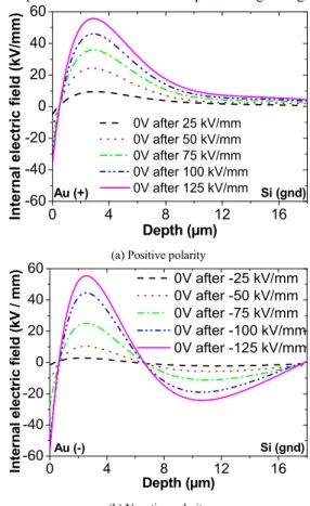
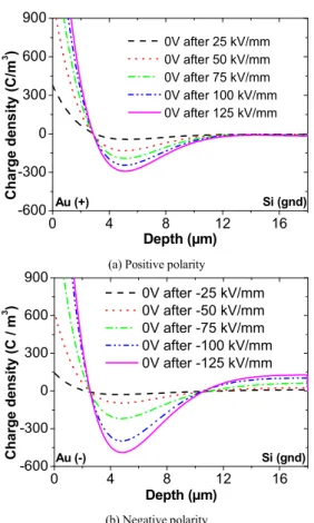
Fig. 3 and Fig. 4 represent respectively the internal electric field and space charge distribution obtained on Au/PI-18 µm samples by the LIMM after deconvolution. Profiles analyzed herein were obtained 10 min after the polarization switch off. Results are shown for both polarities. It is important to note that the space charge magnitude
0 4 8 12 16 -60 -40 -20 0 20 40 60 In te rn al elec tr ic f iel d (kV/ mm) Depth (µm) 0V after 25 kV/mm 0V after 50 kV/mm 0V after 75 kV/mm 0V after 100 kV/mm 0V after 125 kV/mm Si (gnd) Au (+)
(a) Positive polarity
0 4 8 12 16 -60 -40 -20 0 20 40 60 In ternal el ectri c f iel d (kV / m m ) Depth (µm) 0V after -25 kV/mm 0V after -50 kV/mm 0V after -75 kV/mm 0V after -100 kV/mm 0V after -125 kV/mm Au (-) Si (gnd) (b) Negative polarity
Fig. 3. Internal electric field distribution at different DC voltages for both polarities – Au/PI-18 µm structure.
contains some errors close to top electrode surface compared to the deeper side.
When a positive voltage is applied on the top electrode (see Fig. 3a, 4a), negative charges are detected in the bulk of the PI-layer. A build-up of these negative charges occurs as the applied field is increasing. Correspondingly, the internal electric field exhibits increasing values as the external voltage is rising. The residual internal field is negative in the vicinity of the gold electrode and positive in the rest of the sample (providing therefore field intensification under polarization). In addition, it can be noted that the charge is almost zero in the vicinity of the substrate.
When the polarity is reversed (see Fig. 3b, 4b), a build-up of negative charges is still observed in the bulk of the samples, but some positive charges are detected in the vicinity of the wafer, albeit with a smaller amount than
negative charges. Compared to the positive polarity, negative charge amount is clearly higher for the negative polarity. Furthermore, the residual internal field becomes positive in the vicinity of the Si-wafer.
Fig. 5 represents the DC conductivity plotted versus the applied electric field for both polarities as obtained on samples with the structure Au/PI-18 µm. The error bars have been calculated from the dispersion of current data.
For Au/PI-18 µm samples, under both polarities, the DC conductivity exhibits increasing values with the external electric field.
B. Influence of the PI-layer thickness on the electrical behavior of PI
Fig. 6 represents the internal electric field distributions for Au/PI samples with a thickness of 12 and 18 µm after 1h of polarization at ±125 kV/mm. The impact of the PI thickness is seen mainly on the field profiles, hence the choice of representation done in Fig. 6. The internal electric field profile is similar for both thicknesses whichever the polarity. The main difference is at the level of the positive maximum value: the thicker the PI-film, the higher the internal field intensity for both polarities.
The DC conductivity versus the electric field for 12 µm-thick and 18 µm-µm-thick samples is plotted in Fig. 7. The conductivity is increased when the PI-layer is thinner. Liang
et al. reported also this trend on the conduction current [5].
-150 -100 -50 0 50 100 150 10-18 10-17 10-16 10-15 PI 18µm - Au (+) PI 18µm - Au (-) DC con duct ivi ty ( S /c m )
Applied electric field (kV/mm)
Fig. 5. DC conductivity vs. applied electric field for both polarities – Au/PI-18 µm. 0 4 8 12 16 -600 -300 0 300 600 900 Ch ar g e d en sit y (C/m 3 ) Depth (µm) 0V after 25 kV/mm 0V after 50 kV/mm 0V after 75 kV/mm 0V after 100 kV/mm 0V after 125 kV/mm Au (+) Si (gnd)
(a) Positive polarity
0 4 8 12 16 -600 -300 0 300 600 900 C h arge density (C / m 3 ) Depth (µm) 0V after -25 kV/mm 0V after -50 kV/mm 0V after -75 kV/mm 0V after -100 kV/mm 0V after -125 kV/mm Au (-) Si (gnd) (b) Negative polarity
Fig. 4. Charge density profile at different DC voltages for both polarities – Au/PI-18 µm structure.
0.0 0.2 0.4 0.6 0.8 1.0 -60 -40 -20 0 20 40 60 In te rn al el ec tr ic f ie ld ( k V/ m m ) Normalized depth (z/L) 0V after 125 kV/mm - 12 µm 0V after 125 kV/mm - 18 µm Au (+) Si (gnd)
(a) Positive polarity
0.0 0.2 0.4 0.6 0.8 1.0 -60 -40 -20 0 20 40 60 Int ern al elect ri c f ield ( kV/m m ) Normalized depth (z/L) 0V after -125 kV/mm - 12 µm 0V after -125 kV/mm - 18 µm Au (-) Si (gnd) (b) Negative polarity
Fig. 6. Internal electric field under a positive (a) and a negative (b) polarity vs. normalized depth (with the thickness of the sample) after
1h of polarization at ±125 kV/mm – Comparison of PI-thicknesses; Au top electrodes.
C. Influence of the electrode material on the electrical behavior of PI
Fig. 8 compares the charge density distributions for samples with a top metallization of Au and Al after 1h of polarization at ±125 kV/mm. Contrary to the thickness, the electrode material has an important impact on the charge density. The shape and magnitude of charge density are similar for both electrodes under a positive polarity. However, for a negative polarity, even if in both cases there are negative charges in the bulk of the PI-layer and positive charges in the vicinity of the Si-substrate, the shapes of profiles are different. The amount of negative charges is clearly smaller when the sample is metallized with Al.
A comparison of the DC conductivity of 18 µm-thick samples provided with Au and Al metallizations is done in
Fig. 9. Surprisingly, the conductivity is similar under a negative polarity but different with a positive polarity, whereas for the space charge study, the impact of the aluminium electrode is observed only under a negative polarity. In contrast, under a positive polarity, the conductivity of the sample metallized with aluminium is clearly higher than the conductivity of samples with a gold electrode.
D. Discussion
In the previous section, the influences of the applied field strength, voltage polarity, electrode nature and PI-thickness have been assessed on the space charge and on the conductivity of PI. The LIMM appears as a suited method to investigate space charge distribution in PI films as thin as 10 - 20 µm in MIS structures.
Whatever the sample structure, the increase in the applied voltage implies a build-up of negative charges in the sample bulk and, as a consequence, an increase of the residual internal field, which is positive. Moreover, whatever the sample structure, the application of a negative polarity on the top electrode generates the presence of positive charges in the vicinity of the silicon substrate and an internal electric field which becomes negative after a normalized depth of around 0.4 here.
Space charge build-up may be due to electronic carrier injection from the electrodes followed by displacement in the bulk. For a positive polarity, the negative charges can result from the injection of electrons from the n-type substrate followed by their drift towards the top electrode. For a negative polarity, electrons must be injected from the gold electrode. The observed positive charges may come from the Si-substrate, explaining the smaller amount.
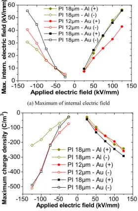
In order to compare the impact of the electrode material and PI thickness, the maximum of negative charge density and maximum of internal electric field – positive – are plotted as a function of the applied electric field and polarity in Fig. 10.
Regarding the PI thickness, the charge profile is similar for both thicknesses. However, the internal electric field is decreased for the lowest thickness under both polarities. In parallel, the conductivity is increased, whatever the polarity and the applied field.
Results from section III.A indicated that under negative polarity, an injection of electrons from the top electrode takes place. The study with the Al electrode is along this
0.0 0.2 0.4 0.6 0.8 1.0 -600 -300 0 300 600 900 Ch ar ge d en sit y ( C /m 3 ) Normalized depth (z/L) 0V after 125 kV/mm - Al 0V after 125 kV/mm - Au Top el (+) Si (gnd)
(a) Positive polarity
0.0 0.2 0.4 0.6 0.8 1.0 -600 -300 0 300 600 900 C h ar ge d e n sity (C /m 3 ) Normalized depth (z/L) 0V after -125 kV/mm - Al 0V after -125 kV/mm - Au Top el (-) Si (gnd) (b) Negative polarity
Fig. 8. Charge density under a positive (a) and a negative (b) polarity vs. normalized depth (with the thickness of the sample) after 1h of polarization at ±125 kV/mm – Comparison of electrode materials;
PI-18 µm. -150 -100 -50 0 50 100 150 10-18 10-17 10-16 10-15 10-14 PI 12µm - Au (+) PI 12µm - Au (-) PI 18µm - Au (+) PI 18µm - Au (-) D C con d u cti vi ty ( S /cm )
Applied electric field (kV/mm)
Fig. 7. DC conductivity vs. applied electric field – Comparison of PI-thicknesses; Au top electrodes.
-150 -100 -50 0 50 100 150 10-18 10-17 10-16 10-15 PI - Al (+) PI - Al (-) PI - Au (+) PI - Au (-) DC co n d uc ti v it y (S /cm )
Applied electric field (kV/mm)
Fig. 9. DC conductivity vs. applied electric field – Comparison of electrode materials; PI-18 µm
direction as it reveals a sensitivity of the amount of stored charge to the nature of electrode. The fact that the stored negative charge amount decreases with the Al electrode could be linked to a change in the barrier to injection. The fact that Al oxidizes rather easily could strengthen the barrier to injection. Indeed, it is known that oxide can act as a barrier against electrons injection [9].
At this level of work, establishing a direct link between space charge dynamics and conduction phenomena is still ongoing.
IV. CONCLUSION
Space charge distribution profiles in PI thin films have been probed by LIMM under DC electric fields in the range ±25 to ±125 kV/mm. Space charge measurements show strong dependence of the response of the PI as a function of
the polarity and of the DC stress. A large increase in negative charges depending on a DC stress was observed under both polarities, which suggests that electron injection from the silicon substrate occurs in PI under a positive polarity and that negative charges can also be injected from the top electrode under a negative polarity. Two thicknesses (12 and 18 µm) of PI-layer and two electrode materials (gold and aluminum) were used and compared. The PI thickness has a substantial impact on the internal electric field enhancement and the conductivity. The native alumina layer formed between the Al top electrode and the polyimide acts very likely as an electronic barrier. Further investigation is necessary to understand the link between conduction phenomena and space charge dynamics.
ACKNOWLEDGMENT
The authors wish to thank B. Schlegel for his kind help in sample preparation.
REFERENCES
[1] S. Zelmat, M.-L. Locatelli, T. Lebey, and S. Diaham, « Investigations on high temperature polyimide potentialities for silicon carbide power device passivation », Microelectron. Eng, vol. 83, pp. 51‑54, 2006. [2] G. Mazzanti, G. C. Montanari, and L. A. Dissado, « Electrical aging
and life models: the role of space charge », IEEE Trans. Dielectr. Electr. Insul., vol. 12, pp. 876‑890, 2005.
[3] K. Kaneko, R. Shiomi, Y. Suzuoki, T. Mizutani, H. Shiota, and H. Muto, « Effects of electrode material on injection and space charge formation in polyimide », Proc. IEEE Internat. Conf. Solid Dielectrics, pp. 518‑521, 2007.
[4] G. M. Sessler, B. Hahn, and D. Y. Yoon, « Electrical conduction in polyimide films », J. Appl. Phys., vol. 60, pp. 318‑326, 1986. [5] T. Liang, Y. Makita, and S. Kimura, « Effect of film thickness on the
electrical properties of polyimide thin films », Polymer, vol. 42, pp. 4867-4872, 2001.
[6] G. Xu, C. C. Gryte, A. S. Nowick, S. Z. Li, Y. S. Pak, and S. G. Greenbaum, « Dielectric relaxation and deuteron NMR of water in polyimide films », J. Appl. Phys., vol. 66, pp. 5290 5296, 1989. [7] S. B. Lang and D. K. Das‐Gupta, « Laser‐intensity‐modulation
method: A technique for determination of spatial distributions of polarization and space charge in polymer electrets », J. Appl. Phys., vol. 59, pp. 2151‑2160, 1986.
[8] A. Petre, D. Marty-Dessus, L. Berquez, and J.-L. Franceschi, « A comparison of different mathematical treatments for solving the inverse problem in focused laser intensity modulation method », Jap. J. Appl. Phys., vol. 43, p. 2572‑2579, 2004.
[9] M. Koehler and I. A. H. Mmelgen, « Tunneling through a metal/polymer interface containing a thin oxide layer: Discussion of the consequences of oxide presence on charge injection », Interface Sci., vol.6, pp. 235–241, 1998. -150 -100 -50 0 50 100 150 0 10 20 30 40 50 60 PI 18µm - Al (+) PI 18µm - Al (-) PI 12µm - Au (+) PI 12µm - Au (-) PI 18µm - Au (+) PI 18µm - Au (-) M ax. in tern. el ect ri c f iel d ( kV /m m )
Applied electric field (kV/mm)
(a) Maximum of internal electric field
-150 -100 -50 0 50 100 150 -500 -400 -300 -200 -100 0 M ax im um char ge densi ty (C /m 3 )
Applied electric field (kV/mm) PI 18µm - Al (+) PI 18µm - Al (-) PI 12µm - Au (+) PI 12µm - Au (-) PI 18µm - Au (+) PI 18µm - Au (-)
(b) Maximum of charge density
Fig. 10. Maximum of internal electric field (a) and of charge density (b) vs. applied electric field for both polarities – Comparison of the three