RESEARCH OUTPUTS / RÉSULTATS DE RECHERCHE
Author(s) - Auteur(s) :
Publication date - Date de publication :
Permanent link - Permalien :
Rights / License - Licence de droit d’auteur :
Institutional Repository - Research Portal
Dépôt Institutionnel - Portail de la Recherche
researchportal.unamur.be
University of Namur
Influence of Native Defects on the Electronic and Magnetic Properties of CVD Grown
MoSe2 Single Layers
Koós, Antal A.; Vancsó, Péter; Szendrö, Márton; Dobrik, Gergely; Antognini Silva, David;
Popov, Zakhar I.; Sorokin, Pavel B.; Henrard, Luc; Hwang, Chanyong; Biró, László P.;
Tapasztó, Levente
Published in:
Journal of Physical Chemistry C DOI:
10.1021/acs.jpcc.9b05921
Publication date: 2019
Document Version
Publisher's PDF, also known as Version of record
Link to publication
Citation for pulished version (HARVARD):
Koós, AA, Vancsó, P, Szendrö, M, Dobrik, G, Antognini Silva, D, Popov, ZI, Sorokin, PB, Henrard, L, Hwang, C, Biró, LP & Tapasztó, L 2019, 'Influence of Native Defects on the Electronic and Magnetic Properties of CVD Grown MoSe2 Single Layers', Journal of Physical Chemistry C, vol. 123, no. 40, pp. 24855-24864.
https://doi.org/10.1021/acs.jpcc.9b05921
General rights
Copyright and moral rights for the publications made accessible in the public portal are retained by the authors and/or other copyright owners and it is a condition of accessing publications that users recognise and abide by the legal requirements associated with these rights. • Users may download and print one copy of any publication from the public portal for the purpose of private study or research. • You may not further distribute the material or use it for any profit-making activity or commercial gain
• You may freely distribute the URL identifying the publication in the public portal ?
Take down policy
If you believe that this document breaches copyright please contact us providing details, and we will remove access to the work immediately and investigate your claim.
In
fluence of Native Defects on the Electronic and Magnetic
Properties of CVD Grown MoSe
2
Single Layers
Antal A. Koós,
*
,†Péter Vancsó,
†,‡Márton Szendrő,
†Gergely Dobrik,
†David Antognini Silva,
‡Zakhar I. Popov,
§,⊥Pavel B. Sorokin,
§,¶Luc Henrard,
‡Chanyong Hwang,
∥László P. Biró,
†and Levente Tapasztó
††Centre for Energy Research, Institute of Technical Physics and Materials Science, Hungarian Academy of Sciences, P.O. Box 49, 1525 Budapest, Hungary
‡Department of Physics, University of Namur, 61 rue de Bruxelles, 5000 Namur, Belgium §National University of Science and Technology MISiS, 119049 Moscow, Russia
∥Korea Research Institute of Standards and Science, Daejeon 305340, Republic of Korea
⊥Emanuel Institute of Biochemical Physics RAS, 4 Kosygina st, Moscow 199339, Russian Federation ¶Moscow Institute of Physics and Technology, 141700, 9 Institutsky lane, Dolgoprudny, Russian Federation
*
S Supporting InformationABSTRACT: Despite their application potential, the struc-ture of CVD grown MoSe2 single layers remained relatively unexplored. Here we report the rotationally aligned CVD growth of MoSe2single layers on graphite. Such MoSe2layers are characterized by grain boundary structures with signi fi-cantly reduced disorder and display a much lower grain boundary density compared to samples grown by MBE. We show that the grain boundaries of CVD MoSe2on graphite are predominantly mirror twin boundaries (MTBs) and distin-guish two classes of such MTBs based on their orientation
relative to the zigzag directions of the MoSe2lattice. By combining atomic resolution scanning tunneling microscopy (STM)
and spectroscopy measurements with DFT calculations, we demonstrate that the predominantly present MTBs running along zigzag directions only slightly perturb the electronic structure of the MoSe2sheet. This enables the CVD growth of large-area
MoSe2layers with high structural and electronic quality. Atomic resolution STM investigations also revealed a high density (1012cm−2) of native point defects identified as Mo vacancies. Our DFT calculations predict that Mo vacancies in MoSe2are
magnetic, and their magnetic moment can be efficiently controlled electrically by tuning the Fermi level position.
1. INTRODUCTION
The unique properties of 2D materials like graphene1 and transition metal dichalcogenides (TMDC)2−4 offer unprece-dented opportunities in a wide range of applications, for example, designing novel electronic devices,5−10 faster sensors,11−14 more efficient catalysts,15 or optoelectronic devices.16 The combination of layered materials in hetero-structures allows us to further improve the applicability of these materials.17 Hybrids of metallic graphene and semi-conducting TMDC,18with a band gap in the visible range of the electromagnetic spectrum, are also excellent candidates to improve the performance of field effect transistors and optoelectronic devices.19−21 Among them, devices based on MoS2are the most widely investigated.22However, transistors based on MoSe2 single layers also demonstrated promising
performance.6,22,23 Furthermore, a series of interesting and potentially useful phenomena have been observed or predicted in MoSe2, such as negative magnetoresistance24 or enhanced
catalytic activity for H2 evolution.25−27 For practical
applications the synthesis of continuous, large-area 2D TMDC layers is required. The chemical vapor deposition (CVD) growth method is one of the most widely investigated techniques to achieve a scalable growth of macroscopic area 2D crystals. However, CVD grown layers also suffer from a few drawbacks as compared to high quality, but microscopic, exfoliated 2D TMDCflakes. In general, CVD grown layers are expected to contain a higher concentration of grain boundaries and native point defects that are known to substantially affect their electronic and optical properties.28To fully understand and optimize the electronic and optoelectronic properties of CVD grown TMD layers, a detailed knowledge of their atomic and electronic structure, particularly regarding their native defects, is essential. For MoS2layers there is a rapidly growing
Received: June 21, 2019 Revised: September 6, 2019 Published: September 9, 2019
Article
pubs.acs.org/JPCC
Cite This:J. Phys. Chem. C 2019, 123, 24855−24864
© 2019 American Chemical Society 24855 DOI:10.1021/acs.jpcc.9b05921
J. Phys. Chem. C 2019, 123, 24855−24864 This is an open access article published under a Creative Commons Attribution (CC-BY)
License, which permits unrestricted use, distribution and reproduction in any medium, provided the author and source are cited.
Downloaded via 81.241.104.23 on March 8, 2021 at 09:22:46 (UTC).
amount of data in this respect,29−35 while MoSe2 layers remained more unexplored.36−38
During the CVD growth, grain boundaries emerge due to the coalescence of various flakes that start to grow from different nucleation sites on the substrate. On most substrates, eachflake starts to grow with random orientation, giving rise to a wide range of grain boundary geometries with various misorientation angles, structure, and electronic properties. Indeed, this has been a major limiting factor for the quality of CVD grown graphene on Cu39−41 or MoS2 on Si/SiO2
substrate.30,35,42These random grain boundaries substantially modify the local atomic and electronic structure, degrading the homogeneity and electronic quality of CVD grown sheets. To avoid this, a better control is needed on the orientation, structure and properties of the grain boundaries. Molecular beam epitaxy (MBE) growth offers a straightforward solution to avoid the disorder emerging from the random flake orientations. However, MoSe2 layers grown by MBE were shown to host a high density of 1D domain boundaries.43,44 The formation of such domain boundaries is attributed to the Mo-rich growth conditions37 and attracted particular atten-tion.45−48In this paper we show that a highly epitaxial growth of MoSe2 single layers can be achieved by the CVD method using graphite as substrate. The CVD grown MoSe2 on
graphite is characterized by 60° mirror twin grain boundaries, while their density is reduced by orders of magnitude as compared to MBE grown MoSe2layers, making CVD grown
samples better candidates for practical applications.
Besides grain boundaries, point defects are also expected to be present in a significant concentration in CVD grown TMDC layers. Chalcogenide vacancies are the most often encountered and investigated point defects that play an important role in defining the optical properties of TMDC crystals. For CVD grown MoS2 single layers, a particularly
strong emission from defect bound excitons was observed in photoluminescence measurements49 that has been attributed to the presence of native chalcogenide atom vacancies. By contrast, in CVD grown MoSe2 samples it has been recently
shown that excitons are captured by point defects other than Se vacancies.50Antisite defects and metal atom vacancies have also been reported in TEM and STM investigations;51,52 however, their concentration is generally expected to be low due to their relatively high formation energies. Here we present experimental results showing that Mo vacancies appeared in high concentration in the CVD growth MoSe2 samples highlighting the importance of the growth kinetics in the CVD method.
2. EXPERIMENTAL AND COMPUTATIONAL METHODS
MoSe2samples were produced by atmospheric pressure CVD in a two-zone tube furnace heated to 400 and 750 °C. The distance between the furnaces was set to 3 mm to avoid overheating of the low-temperature furnace. The furnaces were heated to and cooled from growth temperature without precursors; they were moved into growth position at the beginning of the growth cycle and removed at the end. Therefore, the temperature of the precursors changed significantly in a few seconds, and we could reduce the effect of transition periods. The growth was performed in 20 mm inner diameter quartz tube, with 80 sccm Ar and 20 sccm H2 flow (Messer 99.999% purity). The quartz tube was purged before and after the experiment with Ar. A quartz crucible containing 100 mg of Se (VWR a.r.) was heated in thefirst, low-temperature furnace, from which ∼20 mg of Se was evaporated during 15 min MoSe2 growth. Another quartz
crucible, heated in the high-temperature furnace, contained 25 mg of MoO3 (Alfa Aesar, 99.5%) and supported the highly
Figure 1.(a) STM image (I = 200 pA, V = 1 V) of single-layer MoSe2flakes grown by CVD on a graphite substrate. Inset shows an illustration of the grain boundary formation when two triangularflakes of opposite orientation merge during growth. (b) Atomic resolution image (I = 1 nA, V = −0.1 V) showing a moiré superlattice of 0.98 nm periodicity. The inset shows the calculated total energy gain for different supercells as a function of the rotation angle of the MoSe2lattice relative to the graphite lattice. The observed moiré superlattice corresponds to the geometry having zero rotation and moiré angle.
oriented pyrolytic graphite (HOPG) substrate. The HOPG was freshly cleaved before experiments and placed with the cleaved surface facing down (toward the MoO3precursor).
The STM investigation of the samples was performed using Bruker NanoScope 8 scanning probe microscope with PtIr (80−20%) tip at room temperature. The STM and tunneling spectroscopy measurements have been performed in a N2 atmosphere to avoid the chemical modification of the samples especially during the relatively high bias voltages (±1.5 V) applied during the spectroscopy. The STM images were analyzed with WSxM software.53 The Raman spectra have been recorded by using Witec Alpha 300 Raman system with 532 nm laser excitation and laser power at the sample lower than 0.5 mW.
Calculations were performed in the framework of spin-polarized DFT theory implemented in the VASP software package54 using the plane wave basis set and projector augmented wave method.55 Exchange-correlation effects were taken into account in the framework of generalized gradient approximation (GGA) by the Perdew−Burke−Ernzerhof (PBE) functional.56 Atomic positions were relaxed by using the conjugate-gradient method until the forces of the atoms were reduced to 0.01 eV/Å, and the cutoff energy for the plane-wave basis set was set to be 400 eV. The mirror twin boundaries were modeled in a ribbon geometry37by using a rectangular supercell. To avoid artificial interactions between periodic replicas of the ribbons, a vacuum interval of 15 Å was introduced in the y-direction. Point defects were modeled in 4 × 4 and 6 × 6 supercell geometries. The Brillouin zone was sampled with (8× 1 × 1) and (2 × 2 × 1) Monkhorst−Pack mesh57for geometry optimization and (32× 1 × 1) and (8 × 8 × 1) for density-of-states calculations of the mirror twin boundaries and point defects, respectively.
The formation energy of the native vacancy in MoSe2
monolayer is calculated as
∑
μ = − − E E E N i i iform defect pristine
where Epristineis the total energy per a supercell of a pristine single-layer MoSe2without a defect, Edefectis the total energy of
a single-layer MoSe2containing a defect in the supercell, Niis the number of i elements (Mo and Se) added (or removed) in the supercell for the native defect, and μi is the chemical potential of the element i. The chemical potentialsμMoandμSe
are determined through the condition of the equilibrium with MoSe2:μMo+ 2μSe= E(MoSe2). In the Mo-rich limit condition
the Mo bcc bulk phase and in the Se-rich limit the Se8 molecule were chosen as Mo and Se reservoirs.
3. RESULTS AND DISCUSSION
Figure 1a shows an STM image of MoSe2single-layer flakes
grown by CVD on top of the HOPG substrate. Atomic steps in the graphite substrate are also clearly visible, which often act as preferred nucleation sites for the MoSe2 growth. The lateral sizes of MoSe2 flakes are typically of order of hundreds of
nanometers. Although the MoSe2 flakes are not perfectly triangular in shape, overall, the edges follow the zigzag directions of the MoSe2 lattice as determined by atomic resolution STM images (Figure 1b). This is similar to the case of the CVD grown MoS2triangles35where zigzag edges were found to exhibit a lower formation energy than armchair ones.58,59 Furthermore, it is also apparent that the MoSe2 edges are predominantly running along three preferential
directions, which indicates a rotationally aligned growth with the underlying graphite lattice. Smaller bright spots on top of someflakes are the seeds of the second MoSe2layer. Atomic resolution images (Figure 1b) taken on top of MoSe2 single
layers display a hexagonal lattice of 3.3 Å periodicity, corresponding to the lattice of top Se atoms. Moreover, an additional larger periodicity modulation is superposed on the atomic lattice with a period of 9.8 ± 0.2 Å. This moiré superlattice emerges due to the lattice mismatch between the MoSe2 and graphite. Approximately 3 lattice constants of
MoSe2(3.3 Å) correspond to 4 lattice constants of the graphite (2.45 Å). Of course, the superlattice periodicity is also dependent on the relative rotation of the two lattices. To identify the superstructure and explore the possible rotational states of the system, we analyzed the energetics of different supercells based on a commensuration model. We searched a huge number of geometrically possible commensurate super-cells as described in refs60and61. From these supercells we sorted out the ones that are energetically favorable to form according to the energy competition between the elastic and adhesion energies. In our model the total energy gain per unit area is δ ε = − E Y l d 1 2 2 3 d 2 2
where the first term corresponds to the simple linear elastic deformation of the MoSe2 lattice, Y is the 2D Young’s
modulus, andδ is the required strain of the MoSe2lattice to form a commensurate structure with the graphite substrate. The second term relates to the adhesion energy gain of the commensurate transformation with supercell size l (see details in theSupporting Information).
Our model verifies the 3 Se × 4 C geometry with 9.84 Å periodicity and zero rotational angle between the MoSe2and the graphite lattices. This configuration has the largest total energy gain compared to other supercells (seeFigure 1b, inset) indicating the rotationally fully aligned CVD growth of the MoSe2 on graphite, in excellent agreement with our experi-ments. In contrast, for the case of MoS2 on graphite several
stable rotational configurations have been observed exper-imentally by STM measurements,62−65 again in good agree-ment with our theoretical model (Figure S1). Consequently, in contrast to MoS2, for MoSe2fully epitaxial CVD growth can be
achieved on a graphite substrate.
Measuring the height of the MoSe2flakes by STM gives a
0.7 nm value, which is consistent with the single-layer height. However, the measured height can vary substantially as a function of the imaging conditions (bias voltage) similar to the case of MoS2flakes on graphite.66We also performed confocal
Raman spectroscopy measurements revealing the expected peak of MoSe2single layer (with small bilayer areas) at 241±
0.5 cm−1(Figure S2).67
In the STM image in Figure 1a it is apparent that bright linear features are often present within the MoSe2flakes. Such line defects can be attributed to grain boundaries and are formed when two triangular single-layerflakes growing from different nucleation sites laterally grow together. The boundaries along which different flakes are joined together remain visible in the STM images. One can note that the orientation of such boundaries is most often parallel with the edges of the triangular flakes, implying that they are predominantly running along the zigzag directions of the MoSe2lattice. This preference is also apparent on theflake in
The Journal of Physical Chemistry C Article
DOI:10.1021/acs.jpcc.9b05921
J. Phys. Chem. C 2019, 123, 24855−24864
the middle of the STM image inFigure 1a, where two zigzag grain boundaries are present within theflake instead of a single armchair boundary. We were able to achieve atomic resolution STM images on or around several MoSe2grain boundaries, as
shown in Figure 2a,b. To obtain atomic resolution STM images, we cleaned the imaged area by sweeping the adsorbates away through repeated scanning. Fortunately, at room temperature adsorbed molecules are rather mobile, and they can be removed by the mechanical tip−sample interaction during scanning at small tip−sample distances. We have shown previously that only covalently bound environmental species are detectable by STM at room temperature on TMDC surfaces.68 Atomic resolution STM images evidence that the atomic lattices on the two sides of a MoSe2 grain boundary
have closely matching orientations. This is further confirmed by 2D Fourier transformed images (FFT) revealing that indeed the orientation of the atomic (and moiré) lattices on the two sides of the grain boundary coincides within experimental error (see e.g. inset ofFigure 2a). This matching orientation clearly evidences the rotationally fully aligned CVD growth of MoSe2
on graphite, predicted also by our theoretical calculations. This leads to the prevalence of a special class of grain boundaries. As can be seen fromFigure 1a, grain boundaries often originate from the coalescence of two triangularflakes with a relative in-plane rotation of 180°. Because of the 3-fold symmetry of the MoSe2 lattice, the resulting GBs have a 60° tilt angle, also
called mirror twin boundaries (MTB)69 where only the positions of Mo and Se lattice sites have been swapped in the two grains (see e.g. Figure 3 insets). Therefore, the rotationally aligned growth is expected to yield more regular grain boundaries as compared to the ones joining randomly oriented grains. Our atomic resolution STM measurements on various MoSe2 GBs confirmed that they are prevalently (>90%) mirror twin boundaries, where atomic lattices on the two sides of the boundary have the same lattice orientation. Furthermore, the observed MTBs are predominantly (∼80%) running along the zigzag lattice directions (Figure 2a, 0°), with a few notable exceptions when they enclose afinite angle with the zigzag orientation (Figure 2b, 5° and 22°). We found that MTBs running along the zigzag directions are highly ordered, while those enclosing an angle with the zigzag direction (but still preserving the rotational alignment of the two sides) are characterized by a more disordered atomic structure. In the latter case it was not possible to achieve atomic resolution on the grain boundaries themselves. This is due to a much stronger local perturbation of their electronic structure.
While disordered structures corresponding to MTBs with nonzero angle respective to the zigzag direction have been often observed in CVD grown MoS2 on graphene and graphite,32,65 the existence and prevalence of the zigzag MTBs with highly ordered atomic structure is a novel characteristic of CVD grown MoSe2on graphite with a high
Figure 2.Atomic resolution STM images (I = 1 nA, V =−0.1 V) (a) revealing the highly ordered structure of a MoSe2mirror twin grain boundary running along the zigzag crystallographic orientation of the MoSe2lattice. The inset shows the corresponding 2D Fourier transformed image. (b) Mirror twin grain boundaries with rotational alignment of the two sides but having various angles relative to the zigzag direction (c) Representative tunneling spectra of various grain boundaries recorded both at forward and backward voltage sweeps.
practical relevance for the CVD growth of large-area TMDC layers of high structural quality.
To get insight into the electronic structure of the MoSe2 grain boundaries, we have also performed tunneling spectros-copy measurements on various GBs (Figure 2c). The tunneling spectra recorded on the defect-free regions of the 2D MoSe2
layer display semiconductor behavior with a band gap of about 1.9± 0.1 eV and an n-doped character (VB ∼ −1.1 eV, CB ∼ +0.8 eV), in good agreement with tunneling spectra of MBE grown MoSe2 films on graphite and bilayer graphene
substrates.70 Tunneling spectra on more disordered MTBs enclosing a nonzero angle with the zigzag crystallographic direction display a substantially reduced band gap of about 1 eV or even below. This is due to emerging midgap electronic defect states, evidencing a substantial modification in the local electronic properties, in correlation with their more disordered atomic structure revealed by topographic STM images. The electronic states observed in the band gap are in remarkably
good agreement with those measured on similar types of grain boundaries in MoS2, where electronic states appeared close to
the valence band in non-zigzag MTBs.32By contrast, tunneling spectra acquired by us on zigzag MTBs (zzMTBs) reveal the absence of strong and well-defined electronic states inside the band gap; only a very weak nonzero density of states is revealed inside the otherwise unmodified band gap. This evidence that zzMTBs, characteristic of CVD grown MoSe2on graphite, do not modify drastically the electronic properties of MoSe2single layers.
To understand the electronic properties of the experimen-tally observed zzMTBs in more details, we have performed DFT calculations on several possible zzMTB geometries. In MoSe2the zigzag edge orientation of the growing triangles can
be either molybdenum zigzag (Mo-zz) or selenium zigzag (Se-zz). Mo-zz triangular edges induce Se-zz MTB interfaces and vice versa due to the symmetry of the system (seeFigure 3a, inset). Thus, we have performed LDOS and simulated STM image calculations on low-energy zzMTB structures37 includ-ing both Mo-zz and Se-zz orientations.
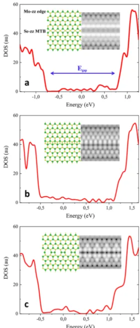
Figure 3 shows the Se-zz MTBs results which have lower formation energies compared to the zz MTBs (for the Mo-zz MTB results see Figure S3). We found that all the investigated Se-zz MTB structures display the characteristics of the pristine MoSe2band gap, with width of 1.4± 0.1 eV. This
indicates that zzMTBS preserves the main features of the DOS spectra of the pristine MoSe2, in excellent agreement with our experimental findings. It is worth noting that DFT PBE calculations underestimate the band gap of single-layer MoSe2 (1.44 eV)71compared to the measured STM gap of around 2 eV.70The observed minor perturbations inside the band gap of zzMTBs are due to the strongly localized metallic states at the boundary.43,44,72The hallmark of these metallic states can be also seen in the spectra of zzMTB (Figure 2c), where inside the band gap weak, but finite, LDOS values were measured. The well-ordered atomic structure in the case of zzMTBs, where neither dangling bonds nor significantly stretched bonds occur, induces significantly less perturbation to the electronic properties than the MTBs enclosing a nonzero angle with the zigzag direction. Indeed, the minor perturbation in such GBs enabled us to acquire atomic resolution STM images, where Se atoms are visible even in the grain boundary region (Figure 2a,b, 0°).
Zigzag MTBs can open the way toward the CVD growth of large-area MoSe2single layers of high structural and electronic
quality. The CVD growth of large-area MoSe2 single layers
comprising only zzMTBs is expected to be much easier to achieve than the growth of macroscopic single crystalline domains. Such samples are expected to largely preserve the quality of MoSe2single crystals, as zzMTBs do not introduce considerable structural or electronic disorder and have significantly reduced density compared to the MBE grown samples, as evidenced by our tunneling microscopy and spectroscopy measurements.
Figure 4a−c displays STM images acquired on the same MoSe2 flake at different bias voltages. At low bias voltages
(−0.1 V) typically used for imaging (Figure 4a), besides the grain boundaries, only faint dark spots can be observed on the 2D MoSe2surface (together with a few bright ones). When the
bias voltage is increased in the negative direction, more bright spots become apparent (Figure 4b). Most strikingly, at high negative bias voltages (−1 V), a high density of bright pointlike features becomes apparent in the STM images (Figure 4c). Figure 3.Calculated atomic and electronic structure of various MoSe2
MTBs with (Se) zigzag orientation. The inset shows the simulated STM images of the corresponding atomic structures.
The Journal of Physical Chemistry C Article
DOI:10.1021/acs.jpcc.9b05921
J. Phys. Chem. C 2019, 123, 24855−24864
Based on their sensitivity to the imaging potential, the origin of these bright spots can be attributed to electronic effects, most likely to the local perturbation of the electronic structure due to structural point defects of the MoSe2lattice. One can note
that some bright spots remain visible independent of the imaging potential. The most likely explanation is a locally shifted Fermi level of the sample, so that the defect state contribution stays within the imaging window even at low bias voltages in some sample areas. A significant spatial variation of the Fermi level within a single TMDCflake has been reported previously.73
To gain more information about the structure of the observed point defects, atomic resolution images are required. In the present sample, we were able to acquire good quality atomic resolution STM images of defects only in the areas where bright defects are visible also at low bias voltages (e.g., ±100 mV). The reason for this is that resolving atomic scale point defects in TMDC single layers is easier at low tip− sample distances33 that require low imaging voltages. The atomic resolution images (Figure 4d,e) reveal that the perturbation of the electronic structure is highly localized over three Se sites. This implies that the center of perturbation is located on a Mo lattice site. We note that defect sites with a Figure 4.(a−c) Bias-dependent STM imaging of CVD grown MoSe2single layers recorded at 200 pA. (d, e) Atomic resolution STM images of point defects in MoSe2. (f) Simulated STM images of Mo and Se vacancy based on their DFT band structure.
Figure 5.(a) Tunneling spectra measured on defect-free MoSe2(blue) and over several point defects (red) revealing the shift of the conduction band and midgap states emerging between−0.4 and −1 V. The main features of the curves recorded on different point defects are similar within experimental error. (b) Calculated local density of states: the blue curve corresponds to the pristine MoSe2 single layer, while the red curve corresponds to the Mo vacancy (VMo).
very similar appearance in the STM images have been observed in MoS2 grown by CVD on a graphite substrate.32
However, their atomic structure has not been fully clarified. To get more insight into the atomic structure of the observed point defects, we have performed DFT calculation of the topographic STM images of possible structural defect sites and compared them with the experimental STM images.
Figure 4f shows theoretical STM images of the two simplest and most commonly encountered point defects: Mo and Se vacancies (for filled/saturated vacancy structures including oxygen substitutions see Figures S4b and S5). Although the most prevalent defects in the TMDC single layer are expected to be chalcogenide atom vacancies and oxygen substitution of chalcogenide vacancies,68,74 the best agreement with our experimental results for topographic images was found for Mo atom vacancies (Figure 4f). This is somewhat surprising, as metal atom vacancies in TMDCs are generally characterized by a high formation energy, making their occurrence less likely. However, these energies might substantially depend on the stoichiometry of the growth conditions. According to our calculations under Se-rich growth conditions, the formation energy of the Mo vacancies (+3.8 eV) approaches that of Se vacancies (+2.6 eV). Se-rich growth conditions can easily occur in a CVD process, as atomic resolution TEM investigation of CVD grown MoSe2 layers also revealed the presence of Mo vacancies in a significant concentration.51The observation of Mo vacancies in CVD grown MoSe2layers by both STM and TEM investigations evidences that not only the formation of point defects in CVD grown samples is determined by energetics but also the growth kinetics plays an important role.
To gain information also on the electronic structure of the observed point defects and the bias dependence of their topographic STM images, we have performed tunneling spectroscopy measurements on defective and defect free areas of the MoSe2 single layer (Figure 5a). The STS measurements were performed after the tip was stable enough, usually after several hours of scanning. Tunneling spectra acquired on the defect-free MoSe2area display semiconductor
behavior with a band gap of about 1.9 eV. By contrast, the tunneling spectra recorded on defective areas display a reduced band gap of about 1.6 ± 0.1 eV, with the conduction band lowered by about 300 meV. Most importantly, on defect sites new electronic states appear within the band gap in the region between −0.4 and −1 V. This observation enables us to interpret the observed bias dependence of the apparent defect density. Because the topographic STM image comprises the integrated LDOS between the Fermi level and the energy corresponding to the imaging bias voltage, the point defects of the MoSe2 layer start to give a significant additional contribution to the tunneling current starting from about −0.4 V and increasing up to −1 eV, where the contrast is expected to be the maximum in good accordance with the measured topographic STM images.
To correlate the experimentally observed tunneling spectra with the atomic structure of the defects, we have performed DFT calculations for the LDOS of the Mo vacancy defects (Figure 5b). From the comparison with the measured tunneling spectra it is clear that the calculated band structure for the Mo vacancies shows a good agreement with the tunneling spectroscopy measurements, both displaying a downshifted conduction band and midgap electronic defect states extending from the valence band deep into the band gap.
By contrast, the Se vacancies and oxygen-filled Se vacancies have a clearly distinct LDOS features (Figure S4). Although the agreement of the LDOS calculations with the measured tunneling spectra is apparent for Mo vacancies, there are some notable differences. The width of the band gap and the position of the Fermi level are clearly different. However, these differences are already present for defect-free MoSe2. The smaller band gap is a general limitation of the DFT description of the MoSe2 band structure at the PBE level rather than a discrepancy with the proposed defect type, while the shifted Fermi level is due to the n-doping of the sample under the experimental conditions. From the STM measurements, we cannot fully exclude the possibility that Mo vacancies arefilled with other atoms, most likely Se, that can give rise to antisite defects (Figure S5a). However, the agreement with the experimental topography and tunneling spectroscopy data is better for empty Mo vacancies. Our DFT calculations also reveal that there is no significant gain in energy upon filling Mo vacancies with Se atoms. The formation energy of the MoSe antisite defects is not considerably lower (+3.6 eV) than that of empty Mo vacancies (+3.8 eV). We also note that Se vacancies might also be present. However, as we have shown in the case of 2D MoS2 crystals,33 clearly resolving single chalcogenide atom vacancies by STM is challenging.
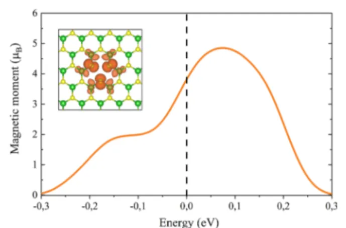
To explore the electronic structure of Mo vacancies in more detail, we have calculated the spin-resolved DFT band structure of Mo vacancies in MoSe2single layers, revealing a strong spin polarization around the Mo vacancy sites. Our calculations reveal that Mo vacancies in undoped MoSe2single layers are characterized by an∼4 μBmagnetic moment, mostly
localized on the nearest-neighbor Se and Mo atoms (inset of
Figure 6). This is in good agreement with previous theoretical
findings.8
Surprisingly, transition metal atom vacancies in other 2D TMDC crystals such as MoS2, MoTe2, or WS2 are not expected to display spin polarization based on previous theoretical results.8,75 Therefore, CVD grown MoSe2 single layers can provide a suitable platform to exploit magnetism in 2D TMDC crystals given the high native concentration of Mo vacancies of order of 1012 cm−2. We note that CVD grown MoSe2 layers on graphite display a substantial n-doping, shifting the Fermi level above the defect states. Because the magnetic moment emerges from the defect states within the band gap, shifting the Fermi level above or below the defect Figure 6.Calculated evolution of the local magnetic moment of a Mo vacancy site as a function of the Fermi energy. Inset shows the isosurface plot of the spin density of the Mo vacancy at the Fermi level (dashed line) of the undoped system.
The Journal of Physical Chemistry C Article
DOI:10.1021/acs.jpcc.9b05921
J. Phys. Chem. C 2019, 123, 24855−24864
states (completely filling or depleting the defect states) will render Mo vacancies nonmagnetic. However, by tuning the Fermi level position to fall within the energy window of the defect states, one can efficiently control the magnetic moment of each Mo vacancy between 0 and∼5 μB(Figure 6), enabling
an efficient electrical control of the magnetism in 2D MoSe2 crystals.
4. CONCLUSIONS
We have shown that the CVD growth of high quality MoSe2
single layers can be achieved on graphite, with MoSe2crystals fully aligned to the underlying graphite lattice, and characterized by highly ordered grain boundary structures. We found that the characteristic mirror twin boundaries running along the zigzag crystallographic direction of the MoSe2 lattice only slightly perturb the atomic and electronic structure of the 2D MoSe2 sheet. The advantages of CVD
grown MoSe2 layers are the much lower grain boundary
density compared to MBE grown MoSe2and the significantly reduced structural disorder in grain boundaries compared to other CVD grown TMDC layers. The CVD growth of MoSe2
layers on graphite is more promising than the widely investigated CVD MoS2 layers due to the prevalence of
ordered zigzag MTB with little influence on the electronic structure of MoSe2. By contrast, the MTBs of various
orientations characteristic of CVD grown MoS2 on graphite
significantly modify the local band gap of the material. These findings open the way toward the CVD growth of large-area MoSe2 single layers of high structural and electronic quality. Tunneling microscopy and spectroscopy investigations also revealed a relatively large (1012cm−2) concentration of single Mo atom vacancies. Such vacancies are predicted to become magnetic, and their magnetic moment can be electrically controlled by tuning the Fermi level. While grain boundaries play a major role in defining the electronic transport device characteristics of CVD grown MoSe2 single layers, Mo
vacancies are expected to enable an efficient engineering of their magnetic and optical properties.
■
ASSOCIATED CONTENT*
S Supporting InformationThe Supporting Information is available free of charge on the
ACS Publications websiteat DOI:10.1021/acs.jpcc.9b05921. Energetic model of commensuration, Raman spectrum; calculated atomic and electronic structure of various MoSe2MTBs; optimized geometries and calculated local
density of states of the defects (PDF)
■
AUTHOR INFORMATION Corresponding Author *[email protected]. ORCID Antal A. Koós: 0000-0003-0563-948X Pavel B. Sorokin:0000-0001-5248-1799 Chanyong Hwang: 0000-0002-6612-7552 Levente Tapasztó:0000-0002-9377-8465 NotesThe authors declare no competingfinancial interest.
■
ACKNOWLEDGMENTSThe work has been supported by the NanoFab2D ERC Starting Grant, the H2020 Graphene Core2 project no. 785219, Graphene Flagship, and the Korea Hungary Joint Laboratory for Nanosciences. A.K. acknowledges the Janos Bolyai Research Fellowship of the Hungarian Academy of Sciences. P.V. acknowledges the Hungarian National Research, Development and Innovation Office (Hungary) Grant No. KH130413. This research used resources of the “Plateforme Technologique de Calcul Intensif (PTCI)”, which was supported by the F.R.S.-FNRS under Convention No. 2.5020.11. P.B.S. and Z.I.P. were supported by Ministry of Education and Science of the Russian Federation in the framework of Increase Competitiveness Program of NUST “MISiS” (No. K2-2017-001). P.B.S. acknowledges the financial support of the Grant of President of Russian Federation for government support of young DSc. (MD-1046.2019.2).
■
REFERENCES(1) Geim, A. K.; Novoselov, K. S. The Rise of Graphene. Nat. Mater. 2007, 6, 183−191.
(2) Tang, Q.; Zhou, Z. Graphene-Analogous Low-Dimensional Materials. Prog. Mater. Sci. 2013, 58, 1244−1315.
(3) Butler, S. Z.; Hollen, S.; Cao, M.; Cui, L. Y.; Gupta, J. A.; Gutiérrez, H. R.; Heinz, T. F.; Hong, S. S.; Huang, J.; Ismach, A. F. Progress, Challenges, and Opportunities in Two-Dimensional Materials Beyond Graphene. ACS Nano 2013, 7, 2898−2926.
(4) Lv, R.; Robinson, J. A.; Schaak, R. E.; Sun, D.; Sun, Y.; Mallouk, T. E.; Terrones, M. Transition Metal Dichalcogenides and Beyond: Synthesis, Properties, and Applications of Single- and Few-Layer Nanosheets. Acc. Chem. Res. 2015, 48, 56−64.
(5) Wang, Q. H.; Kalantar-Zadeh, K.; Kis, A.; Coleman, J. N.; Strano, M. S. Electronics and Optoelectronics of Two-Dimensional Transition Metal Dichalcogenides. Nat. Nanotechnol. 2012, 7, 699− 712.
(6) Larentis, S.; Fallahazad, B.; Tutuc, E. Field-Effect Transistors and Intrinsic Mobility in Ultra-Thin MoSe2 Layers. Appl. Phys. Lett. 2012, 101, 223104.
(7) Radisavljevic, B.; Radenovic, A.; Brivio, J.; Giacometti, V.; Kis, A. Single-Layer MoS2 Transistors. Nat. Nanotechnol. 2011, 6, 147−150. (8) Ma, Y.; Dai, Y.; Guo, M.; Niu, C.; Lu, J.; Huang, B. Electronic and Magnetic Properties of Perfect, Vacancy-Doped, and Nonmetal Adsorbed MoSe2, MoTe2 and WS2 monolayers. Phys. Chem. Chem. Phys. 2011, 13, 15546−15553.
(9) Ma, Y.; Dai, Y.; Wei, W.; Niu, C.; Yu, L.; Huang, B. First-Principles Study of the Graphene@MoSe2 Heterobilayers. J. Phys. Chem. C 2011, 115, 20237−20241.
(10) Souza, E. S.; Scopel, W. L.; Miwa, R. H. Probing the Local Interface Properties at a Graphene-MoSe2 in-Plane Lateral Hetero-structure: An ab Initio Study. Phys. Chem. Chem. Phys. 2018, 20, 17952−17960.
(11) Lopez-Sanchez, O.; Lembke, D.; Kayci, M.; Radenovic, A.; Kis, A. Ultrasensitive Photodetectors Based on Monolayer MoS2. Nat. Nanotechnol. 2013, 8, 497−501.
(12) Liu, H.; Chen, Z.; Chen, X.; Chu, S.; Huang, J.; Peng, R. Terahertz Photodetector Arrays Based on a Large Scale MoSe2Mo-nolayer. J. Mater. Chem. C 2016, 4, 9399−9404.
(13) Abderrahmane, A.; Ko, P. J.; Thu, T. V.; Ishizawa, S.; Takamura, T.; Sandhu, A. High Photosensitivity Few-layered MoSe2 Back-Gated Field-Effect Phototransistors. Nanotechnology 2014, 25, 365202.
(14) Baek, J.; Yin, D.; Liu, N.; Omkaram, I.; Jung, C.; Im, H.; Hong, S.; Kim, S. M.; Hong, Y. K.; Hur, J.; et al. A Highly Sensitive Chemical Gas Detecting Transistor Based on Highly Crystalline CVD-Grown MoSe2 Films. Nano Res. 2017, 10, 1861−1871.
(15) Chhowalla, M.; Shin, H. S.; Eda, G.; Li, L.-J.; Loh, K. P.; Zhang, H. The Chemistry of Two-dimensional Layered Transition Metal Dichalcogenide Nanosheets. Nat. Chem. 2013, 5, 263−275.
(16) Eftekhari, A. Molybdenum Diselenide (MoSe2) for Energy Storage, Catalysis, and Optoelectronics. Appl. Mater. Today 2017, 8, 1−17.
(17) Novoselov, K. S.; Falko, V. I.; Colombo, L.; Gellert, P. R.; Schwab, M. G.; Kim, K. A Roadmap for Graphene. Nature 2012, 490, 192−200.
(18) Roldan, R.; Silva-Guillen, J. A.; Lopez-Sancho, M. P.; Guinea, F.; Cappelluti, E.; Ordejon, P. Electronic Properties of Single-Layer and Multilayer Transition Metal Dichalcogenides MX2 (M = Mo, W and X = S, Se). Ann. Phys. (Berlin, Ger.) 2014, 526, 347−357.
(19) Li, Y.; Wang, Y.; Huang, L.; Wang, X.; Li, X.; Deng, H.-X.; Wei, Z.; Li, J. Anti-Ambipolar Field-Effect Transistors Based on Few-Layer 2D Transition Metal Dichalcogenides. ACS Appl. Mater. Interfaces 2016, 8, 15574−15581.
(20) Cao, W.; Kang, J.; Sarkar, D.; Liu, W.; Banerjee, K. 2D Semiconductor FETs - Projections and Design for Sub-10 nm VLSI. IEEE Trans. Electron Devices 2015, 62, 3459−3469.
(21) Podzorov, V.; Gershenson, M. E.; Kloc, Ch.; Zeis, R.; Bucher, E. High-Mobility Field-Effect Transistors Based on Transition Metal Dichalcogenides. Appl. Phys. Lett. 2004, 84, 3301−3303.
(22) Chuang, H.-J.; Chamlagain, B.; Koehler, M.; Perera, M. M.; Yan, J.; Mandrus, D.; Tománek, D.; Zhou, Z. Low-Resistance 2D/2D Ohmic Contacts: A Universal Approach to High-Performance WSe2, MoS2, and MoSe2 Transistors. Nano Lett. 2016, 16, 1896−1902.
(23) Das, S. R.; Kwon, J.; Prakash, A.; Delker, C. J.; Das, S.; Janes, D. B. Low-Frequency Noise in MoSe2 Field Effect Transistors. Appl. Phys. Lett. 2015, 106, 083507.
(24) Dau, M. T.; Vergnaud, C.; Marty, A.; Rortais, F.; Beigné, C.; Boukari, H.; Bellet-Amalric, E.; Guigoz, V.; Renault, O.; Alvarez, C.; et al. Millimeter-Scale Layered MoSe2 Grown on Sapphire and Evidence for Negative Magnetoresistance. Appl. Phys. Lett. 2017, 110, 011909.
(25) Shu, H.; Zhou, D.; Li, F.; Cao, D.; Chen, X. Defect Engineering in MoSe2 for the Hydrogen Evolution Reaction: From Point Defects to Edges. ACS Appl. Mater. Interfaces 2017, 9, 42688−42698.
(26) Dai, C.; Zhou, Z.; Tian, C.; Li, Y.; Yang, C.; Gao, X.; Tian, X. Large-Scale Synthesis of Graphene-Like MoSe2 Nanosheets for Efficient Hydrogen Evolution Reaction. J. Phys. Chem. C 2017, 121, 1974−1981.
(27) Tsai, C.; Chan, K.; Abild-Pedersen, F.; Nørskov, J. K. Active Edge Sites in MoSe2 and WSe2 Catalysts for the Hydrogen Evolution Reaction: A Density Functional Study. Phys. Chem. Chem. Phys. 2014, 16, 13156−13164.
(28) Hong, J.; Hu, Z.; Probert, M.; Li, K.; Lv, D.; Yang, X.; Gu, L.; Mao, N.; Feng, Q.; Xie, L.; et al. Exploring Atomic Defects in Molybdenum Disulphide Monolayers. Nat. Commun. 2015, 6, 6293. (29) Zhou, W.; Zou, X.; Najmaei, S.; Liu, Z.; Shi, Y.; Kong, J.; Lou, J.; Ajayan, P. M.; Yakobson, B. I.; Idrobo, J.-C. Intrinsic Structural Defects in Monolayer Molybdenum Disulfide. Nano Lett. 2013, 13, 2615−2622.
(30) Najmaei, S.; Liu, Z.; Zhou, W.; Zou, X.; Shi, G.; Lei, S.; Yakobson, B. I.; Idrobo, J.-C.; Ajayan, P. M.; Lou, J. Vapour Phase Growth and Grain Boundary Structure of Molybdenum Disulphide Atomic Layers. Nat. Mater. 2013, 12, 754−759.
(31) Lin, Y. C.; Dumcenco, D. O.; Komsa, H. P.; Niimi, Y.; Krasheninnikov, A. V.; Huang, Y. S.; Suenaga, K. Properties of Individual Dopant Atoms in Single-Layer MoS2: Atomic Structure, Migration, and Enhanced Reactivity. Adv. Mater. 2014, 26, 2857− 2861.
(32) Liu, X.; Balla, I.; Bergeron, H.; Hersam, M. C. Point Defects and Grain Boundaries in Rotationally Commensurate MoS2 on Epitaxial Graphene. J. Phys. Chem. C 2016, 120, 20798−20805.
(33) Vancsó, P.; Magda, G. Z.; Pető, J.; Noh, J.-Y.; Kim, Y.-S.; Hwang, C.; Biró, L. P.; Tapasztó, L. The Intrinsic Defect Structure of Exfoliated MoS2 Single Layers Revealed by Scanning Tunneling Microscopy. Sci. Rep. 2016, 6, 29726.
(34) Wu, K.; Li, Z.; Tang, J.; Lv, X.; Wang, H.; Luo, R.; Liu, P.; Qian, L.; Zhang, S.; Yuan, S. Controllable Defects Implantation in MoS2 Grown by Chemical Vapor Deposition for Photoluminescence Enhancement. Nano Res. 2018, 11, 4123−4132.
(35) van der Zande, A. M.; Huang, P. Y.; Chenet, D. A.; Berkelbach, T. C.; You, Y. M.; Lee, G.-H.; Heinz, T. F.; Reichman, D. R.; Muller, D. A.; Hone, J. C. Grains and Grain Boundaries in Highly Crystalline Monolayer Molybdenum Disulphide. Nat. Mater. 2013, 12, 554−561. (36) Shafqat, A.; Iqbal, T.; Majid, A. A DFT Study of Intrinsic Point Defects in Monolayer MoSe2. AIP Adv. 2017, 7, 105306.
(37) Lehtinen, O.; Komsa, H.-P.; Pulkin, A.; Whitwick, M. B.; Chen, M.-W.; Lehnert, T.; Mohn, M. J.; Yazyev, O. V.; Kis, A.; Kaiser, U.; Krasheninnikov, A. V. Atomic Scale Microstructure and Properties of Se-Deficient Two-Dimensional MoSe2. ACS Nano 2015, 9, 3274− 3283.
(38) Meng, Y.; Ling, C.; Xin, R.; Wang, P.; Song, Y.; Bu, H.; Gao, S.; Wang, X.; Song, F.; Wang, J.; Wang, X.; Wang, B.; Wang, G. Repairing Atomic Vacancies in Single-Layer MoSe2 Field-Effect Transistor and its Defect Dynamics. npj Quantum Mater. 2017, 2, 16.
(39) Huang, P. Y.; Ruiz-Vargas, C. S.; van der Zande, A. M.; Whitney, W. S.; Levendorf, M. P.; Kevek, J. W.; Garg, S.; Alden, J. S.; Hustedt, C. J.; Zhu, Y.; Park, J.; et al. Grains and Grain Boundaries in Single-Layer Graphene Atomic Patchwork Quilts. Nature 2011, 469, 389−392.
(40) Yu, Q.; Jauregui, L. A.; Wu, W.; Colby, R.; Tian, J.; Su, Z.; Cao, H.; Liu, Z.; Pandey, D.; Wei, D.; et al. Control and Characterization of Individual Grains and Grain Boundaries in Graphene Grown by Chemical Vapour Deposition. Nat. Mater. 2011, 10, 443−449.
(41) Biró, L. P.; Lambin, P. Grain Boundaries in Graphene Grown by Chemical Vapor Deposition. New J. Phys. 2013, 15, 035024.
(42) Ly, T. H.; Perello, D. J.; Zhao, J.; Deng, Q.; Kim, H.; Han, G.; Chae, S. H.; Jeong, H. Y.; Lee, Y. H. Misorientation-Angle-Dependent Electrical Transport Across Molybdenum Disulfide Grain Boundaries. Nat. Commun. 2016, 7, 10426.
(43) Liu, H.; Jiao, L.; Yang, F.; Cai, Y.; Wu, X.; Ho, W.; Gao, C.; Jia, J.; Wang, N.; Fan, H.; et al. Dense Network of One-Dimensional Midgap Metallic Modes in Monolayer MoSe2 and Their Spatial Undulations. Phys. Rev. Lett. 2014, 113, 066105.
(44) Barja, S.; Wickenburg, S.; Liu, Z.-F.; Zhang, Y.; Ryu, H.; Ugeda, M. M.; Hussain, Z.; Shen, Z.-X.; Mo, S.-K.; Wong, E.; et al. Charge Density Wave Order in 1D Mirror Twin Boundaries of Single-Layer MoSe2. Nat. Phys. 2016, 12, 751−756.
(45) Jiao, L.; Liu, H. J.; Chen, J. L.; Yi, Y.; Chen, W. G.; Cai, Y.; Wang, J. N.; Dai, X. Q.; Wang, N.; Ho, W. K.; et al. Molecular-Beam Epitaxy of Monolayer MoSe2: Growth Characteristics and Domain Boundary Formation. New J. Phys. 2015, 17, 053023.
(46) Liu, H.; Zheng, H.; Yang, F.; Jiao, L.; Chen, J.; Ho, W.; Gao, C.; Jia, J.; Xie, M. Line and Point Defects in MoSe2 Bilayer Studied by Scanning Tunneling Microscopy and Spectroscopy. ACS Nano 2015, 9, 6619−6625.
(47) Ma, Y.; Diaz, H. C.; Avila, J.; Chen, C.; Kalappattil, V.; Das, R.; Phan, M.-H.; Cadez, T.; Carmelo, J. M. P.; Asensio, M. C.; Batzill, M. Angle Resolved Photoemission Spectroscopy Reveals Spin Charge Separation in Metallic MoSe2 Grain Boundary. Nat. Commun. 2017, 8, 14231.
(48) Ma, Y.; Kolekar, S.; Coy Diaz, H.; Aprojanz, J.; Miccoli, I.; Tegenkamp, C.; Batzill, M. Metallic Twin Grain Boundaries Embedded in MoSe2 Monolayers Grown by Molecular Beam Epitaxy. ACS Nano 2017, 11, 5130−5139.
(49) Amani, M.; Burke, R. A.; Ji, X.; Zhao, P.; Lien, D.-H.; Taheri, P.; Ahn, G. H.; Kirya, D.; Ager, J. W.; Yablonovitch, E.; et al. High Luminescence Efficiency in MoS2 Grown by Chemical Vapor Deposition. ACS Nano 2016, 10, 6535−6541.
(50) Chen, K.; Ghosh, R.; Meng, X.; Roy, A.; Kim, J.-S.; He, F.; Mason, S. C.; Xu, X.; Lin, J.-F.; Akinwande, D.; Banerjee, S. K.; Wang, Y. Experimental Evidence of Exciton Capture by Mid-Gap Defects in CVD Grown Monolayer MoSe2. npj 2D Mater. Appl. 2017, 1, 15.
(51) Gao, D.; Xia, B.; Wang, Y.; Xiao, W.; Xi, P.; Xue, D.; Ding, J. Dual-Native Vacancy Activated Basal Plane and Conductivity of
The Journal of Physical Chemistry C Article
DOI:10.1021/acs.jpcc.9b05921
J. Phys. Chem. C 2019, 123, 24855−24864
MoSe2 with High-Efficiency Hydrogen Evolution Reaction. Small 2018, 14, 1704150.
(52) Guguchia, Z.; Kerelsky, A.; Edelberg, D.; Banerjee, S.; von Rohr, F.; Scullion, D.; Augustin, M.; Scully, M.; Rhodes, D. A.; Shermadini, Z.; Luetkens, H.; Shengelaya, A.; Baines, C.; Morenzoni, E.; Amato, A.; Hone, J. C.; Khasanov, R.; Billinge, S. J. L.; Santos, E.; Pasupathy, A. N.; Uemura, Y. J. Magnetism in Semiconducting Molybdenum Dichalcogenides. Sci. Adv. 2018, 4, 3672.
(53) Horcas, I.; Fernández, R.; Gómez-Rodríguez, J. M.; Colchero, J.; Gómez-Herrero, J.; Baro, A. M. WSXM: A software for Scanning Probe Microscopy and a Tool for Nanotechnology. Rev. Sci. Instrum. 2007, 78, 013705.
(54) Kresse, G.; Joubert, D. From Ultrasoft Pseudopotentials to the Projector Augmented-Wave Method. Phys. Rev. B: Condens. Matter Mater. Phys. 1999, 59, 1758−1775.
(55) Blöchl, P. E. Projector Augmented-Wave Method. Phys. Rev. B: Condens. Matter Mater. Phys. 1994, 50, 17953−17979.
(56) Perdew, J. P.; Burke, K.; Ernzerhof, M. Generalized Gradient Approximation Made Simple. Phys. Rev. Lett. 1996, 77, 3865−3868.
(57) Monkhorst, H. J.; Pack, J. D. Special Points for Brillouin-Zone Integrations. Phys. Rev. B 1976, 13, 5188−5192.
(58) Han, Y.; Hu, T.; Li, R.; Zhou, J.; Dong, J. Stabilities and Electronic Properties of Monolayer MoS2 With One or Two Sulfur Line Vacancy Defects. Phys. Chem. Chem. Phys. 2015, 17, 3813−3819. (59) Byskov, L. S.; Nørskov, J. K.; Clausen, B. S.; Topsøe, H. Edge Termination of MoS2 and CoMoS Catalyst Particles. Catal. Lett. 2000, 64, 95−99.
(60) Merino, P.; Svec, M.; Pinardi, A. L.; Otero, G.; Martín-Gago, J. A. Strain-Driven Moiré Superstructures of Epitaxial Graphene on Transition Metal Surfaces. ACS Nano 2011, 5, 5627.
(61) Meng, L.; Wu, R.; Zhang, L.; Li, L.; Du, S.; Wang, Y.; Gao, H. Multi-Oriented Moiré Superstructures of Graphene on Ir(111): Experimental Observations and Theoretical Models. J. Phys.: Condens. Matter 2012, 24, 314214.
(62) Lu, C.-I.; Butler, C. J.; Huang, J.-K.; Chu, Y.-H.; Yang, H.-H.; Wei, C.-M.; Li, L.-J.; Lin, M.-T. Moiré-Related in-Gap States in a Twisted MoS2/Graphite Heterojunction. npj 2D Mater. Appl. 2017, 1, 24.
(63) Huang, Y. L.; Chen, Y.; Zhang, W.; Quek, S. Y.; Chen, C.-H.; Li, L.-J.; Hsu, W.-T.; Chang, W.-H.; Zheng, Y. J.; Chen, W.; et al. Bandgap Tunability at Single-Layer Molybdenum Disulphide Grain Boundaries. Nat. Commun. 2015, 6, 6298.
(64) Koós, A. A.; Vancsó, P.; Magda, G. Z.; Osváth, Z.; Kertész, K.; Dobrik, G.; Hwang, C.; Tapasztó, L.; Bíró, L. P. STM Study of the MoS2 Flakes Grown on Graphite: A Model System for Atomically Clean 2D Heterostructure Interfaces. Carbon 2016, 105, 408−415.
(65) Wang, D.; Yu, H.; Tao, L.; Xiao, W.; Fan, P.; Zhang, T.; Liao, M.; Guo, W.; Shi, D.; Du, S.; et al. Bandgap Broadening at Grain Boundaries in Single-Layer MoS2. Nano Res. 2018, 11, 6102−6019.
(66) Liu, X.; Balla, I.; Bergeron, H.; Campbell, G. P.; Bedzyk, M. J.; Hersam, M. C. Rotationally Commensurate Growth of MoS2 on Epitaxial Graphene. ACS Nano 2016, 10, 1067−1075.
(67) Sha, Y.; Xiao, S.; Zhang, X.; Qin, F.; Gu, X. Layer-by-Layer Thinning of MoSe2 by Soft and Reactive Plasma Etching. Appl. Surf. Sci. 2017, 411, 182−188.
(68) Pető, J.; Ollár, T.; Vancsó, P.; Popov, Z. I.; Magda, G. Z.; Dobrik, G.; Hwang, C.; Sorokin, P. B.; Tapasztó, L. Spontaneous Doping of the Basal Plane of MoS2 Single Layers Through Oxygen Substitution Under Ambient Conditions. Nat. Chem. 2018, 10, 1246− 1251.
(69) Batzill, M. Mirror Twin Grain Boundaries in Molybdenum Dichalcogenides. J. Phys.: Condens. Matter 2018, 30, 493001.
(70) Ugeda, M. M.; Bradley, A. J.; Shi, S.-F.; da Jornada, F. H.; Zhang, Y.; Qiu, D. Y.; Ruan, W.; Mo, S. K.; Hussain, Z.; Shen, Z. X.; et al. Giant Bandgap Renormalization and Excitonic Effects in a Monolayer Transition Metal Dichalcogenide Semiconductor. Nat. Mater. 2014, 13, 1091−1095.
(71) Ding, Y.; Wang, Y.; Ni, J.; Shi, L.; Shi, S.; Tang, W. First Principles Study of Structural, Vibrational and Electronic Properties of
Graphene-Like MX2 (M = Mo, Nb, W, Ta; X = S, Se, Te) Monolayers. Phys. B 2011, 406, 2254−2260.
(72) Zou, X.; Liu, Y.; Yakobson, B. I. Predicting Dislocations and Grain Boundaries in Two-Dimensional Metal-Disulfides from the First Principles. Nano Lett. 2013, 13, 253−258.
(73) McDonnell, S.; Addou, R.; Buie, C.; Wallace, R. M.; Hinkle, C. L. Defect-Dominated Doping and Contact Resistance in MoS2. ACS Nano 2014, 8, 2880−2888.
(74) Barja, S.; Refaely-Abramson, S.; Schuler, B.; Qiu, D. Y.; Pulkin, A.; Wickenburg, S.; Ryu, H.; Ugeda, M. M.; Kastl, C.; Chen, C.; et al. Identifying Substitutional Oxygen as a Prolific Point Defect in Monolayer Transition Metal Dichalcogenides. Nat. Commun. 2019, 10, 3382.
(75) Noh, J.-Y.; Kim, H.; Kim, Y.-S. Stability and Electronic Structures of Native Defects in Single-Layer MoS2. Phys. Rev. B: Condens. Matter Mater. Phys. 2014, 89, 205417.