HAL Id: hal-02111770
https://hal.archives-ouvertes.fr/hal-02111770
Submitted on 26 Apr 2019HAL is a multi-disciplinary open access archive for the deposit and dissemination of sci-entific research documents, whether they are pub-lished or not. The documents may come from teaching and research institutions in France or abroad, or from public or private research centers.
L’archive ouverte pluridisciplinaire HAL, est destinée au dépôt et à la diffusion de documents scientifiques de niveau recherche, publiés ou non, émanant des établissements d’enseignement et de recherche français ou étrangers, des laboratoires publics ou privés.
Dynamic segregation of metallic impurities at SiO 2 /Si
interfaces
A. de Luca, A. Portavoce, M. Texier, N. Burle, B Pichaud
To cite this version:
A. de Luca, A. Portavoce, M. Texier, N. Burle, B Pichaud. Dynamic segregation of metallic impurities at SiO 2 /Si interfaces. Journal of Physics: Conference Series, IOP Publishing, 2013, 471, pp.012029. �10.1088/1742-6596/471/1/012029�. �hal-02111770�
This content has been downloaded from IOPscience. Please scroll down to see the full text.
Download details:
IP Address: 195.221.220.19
This content was downloaded on 02/12/2013 at 11:21
Please note that terms and conditions apply.
Dynamic segregation of metallic impurities at SiO2/Si interfaces
View the table of contents for this issue, or go to the journal homepage for more 2013 J. Phys.: Conf. Ser. 471 012029
(http://iopscience.iop.org/1742-6596/471/1/012029)
Dynamic segregation of metallic impurities at SiO
2/Si
interfaces
A De Luca, A Portavoce, M Texier, N Burle and B Pichaud
IM2NP, UMR7334 CNRS - Aix-Marseille Université, Faculté des Sciences et Techniques, Campus de Saint-Jérôme, Av. Escadrille Normandie Niémen, F-13397 Marseille Cedex, France
E-mail: [email protected]
Abstract. The behaviour of two metallic impurities, iron and tungsten, during oxidation of silicon wafers has been investigated using transmission electron microscopy and atom probe tomography. Metallic contamination has been introduced by implantation of 54Fe at 65 keV and
186
W at 150 keV, with a dose of 1015 at/cm2. Oxidation of Fe-contaminated Si wafer results in the precipitation of iron as β-FeSi2 at the SiO2/Si interface. The presence of these precipitates
hinders the oxidation front which forms silicon pyramidal defects. Further oxidation of the precipitates leads to iron-rich cluster formation in the SiO2 layer, surrounding the pyramids.
Dry oxidation of a tungsten-contaminated Si wafer is characterised by the formation of nanometric spherical precipitates in the Si layer. The size and density of these precipitates versus depth follow the as-implanted W concentration profile.
1. Introduction
With the increasing complexity of the design of the newest generation of transistors, unintentional contamination by metallic impurities, even at low concentration levels, has become one of the major problems in the manufacturing of modern microelectronic devices. In particular, the presence of very small amounts of contaminants in the active area of transistors is enough to have deleterious impact on their electrical properties making them defective. It is thus essential to improve our understanding of metallic contaminant behaviour during the processing of microelectronic devices and, more specifically, at the interfaces of CMOS structures.
In this context, this work aims at a study of the mechanisms of diffusion and precipitation or segregation of two metallic elements at the SiO2/Si interface: iron and tungsten. The parallel study of these two impurities aims to compare and to model the diffusion/precipitation mechanisms of species exhibiting different diffusion behaviours. Indeed, whereas iron diffusion uses an interstitial mechanism and is a fast diffusing species [1], tungsten shows low diffusion rates [1,2] and an unknown diffusion mechanism.
Depending on both the contaminating element and oxidising conditions, various situations have been distinguished. Based on the experimental observations, a qualitative model for the dynamic segregation of metallic impurities in silicon is proposed.
18th Microscopy of Semiconducting Materials Conference (MSM XVIII) IOP Publishing Journal of Physics: Conference Series 471 (2013) 012029 doi:10.1088/1742-6596/471/1/012029
Content from this work may be used under the terms of theCreative Commons Attribution 3.0 licence. Any further distribution of this work must maintain attribution to the author(s) and the title of the work, journal citation and DOI.
2. Experimental details
In this study, 525 µm-thick P-doped (001) Si 54Fe and 186W ions, at a dose of 10
150keV.
In order to study the effect of oxidation temperature and duration under O2 flux for various conditions (900°C for 5
oxidation times were set to grow SiO Post mortem analyses of the such as Cs-corrected HRTEM
STEM (Scanning Transmission Electron Microscop
Tomography). TEM thin foils and APT tips were prepared micromachining using an FEI Helios microscope
Nanomill device. In order to facilitate were prepared by the lift-out preparation was attached to a microtip with its 3000xHR at a temperature of 80 1.2nJ, corresponding to a ISi2+/ISi1+ 3. Results and discussion
3.1. Fe behaviour during dry oxidation Dry oxidation of iron-implanted Si wafers interface. Their diameters rang
precipitates were located at the
precipitates got partly incorporated in the SiO The precipitate structure was
All the precipitates have been identified as 5]. Except for the shorter oxidation
pyramidal-shaped defects (figure silicon huts whose origin was unclear rich clusters incorporated in the SiO
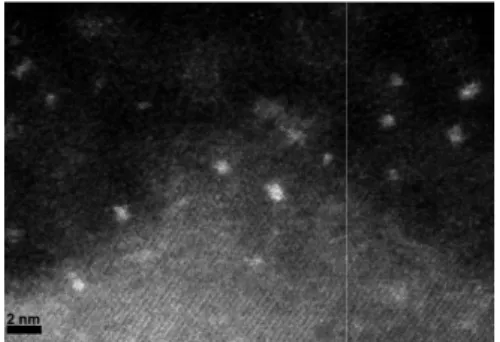
Figure 1. HRTEM image precipitate of β-FeSi2 formed SiO2/Si interface.
Figure 3 shows a pyramidal-shaped defect surmounted by a precipitate. The observed configuration suggests that the formation of those defects is correlated with the presence of a precipitate which locally hinders the propagation of the oxidation front
doped (001) Si wafers (resistivity 2-20 Ω.cm) were
1015 at/cm2 and with implantation energies respectively of 65keV and study the effect of oxidation temperature and duration, the samples were dry oxid
nditions (900°C for 5, 189, 592 min or 1100°C for 12
to grow SiO2 layers with comparable thicknesses for both temperatures. he oxidised specimens were done using several characterisation tools,
(High Resolution Transmission Electron Microscop (Scanning Transmission Electron Microscopy) and LP-APT
(Laser-. TEM thin foils and APT tips were prepared by focused ion beam (DBFIB) FEI Helios microscope. TEM lamellae were cleaned using
. In order to facilitate the evaporation of the oxide layer during APT analysis, preparation method [3] using a specific sample orie
its surface tilted by 10°. APT analyses were carried out
80 K, with a laser pulse frequency of 100 kHz, using a laser power of 1+ ratio of 16.5 and a I
W2+/IW1+ ratio of 5.6.
Fe behaviour during dry oxidation
implanted Si wafers led to the formation of iron precipitates at the SiO ranged from 20 to 50 nm. For the shortest oxidation
re located at the SiO2/Si interface, inside the Si layer. For longer oxidation partly incorporated in the SiO2 layer and became round in shape (figure 1)
was deduced from the Fourier transform (FT) analysis
precipitates have been identified as being the low-temperature stable silicide phase Except for the shorter oxidation time, analysis of the SiO2/Si interface also revealed the
(figure 2), already observed in the literature [4]. These defects
huts whose origin was unclear. HAADF-STEM imaging revealed the presence of small iron incorporated in the SiO2 layer around these pyramids (figure 2).
HRTEM image of a formed at the
Figure 2. HAADF-STEM image showing iron clusters incorporated in the SiO2 layer
pyramidal-shaped defect.
shaped defect surmounted by a precipitate. The observed configuration suggests that the formation of those defects is correlated with the presence of a precipitate which
of the oxidation front.
) were contaminated with respectively of 65keV and he samples were dry oxidised 1100°C for 12 and 44 min). The thicknesses for both temperatures.
using several characterisation tools, (High Resolution Transmission Electron Microscopy), Z-contrast -Pulsed Atom Probe focused ion beam (DBFIB) were cleaned using the Fischione evaporation of the oxide layer during APT analysis, the tips using a specific sample orientation: the wedge carried out with a LEAP K, with a laser pulse frequency of 100 kHz, using a laser power of
the formation of iron precipitates at the SiO2/Si the shortest oxidation times, facetted /Si interface, inside the Si layer. For longer oxidation time, the
(figure 1).
analysis of HRTEM images. temperature stable silicide phase β-FeSi2 [4, /Si interface also revealed the presence of These defects consist of STEM imaging revealed the presence of small
iron-STEM image showing iron clusters layer around a silicon shaped defect surmounted by a precipitate. The observed configuration suggests that the formation of those defects is correlated with the presence of a precipitate which
18th Microscopy of Semiconducting Materials Conference (MSM XVIII) IOP Publishing Journal of Physics: Conference Series 471 (2013) 012029 doi:10.1088/1742-6596/471/1/012029
Figure 3. Filtered HRTEM image showing a pyramidal-shaped defect surmounted by a precipitate, and
associated Fourier
Transform of the original image. Squares indicate selected spots used for filtering.
We thus propose the following model for the formation of these iron-induced defects (figure 4): i) Iron accumulates at the growing SiO2/Si interface forming facetted β-FeSi2 precipitates. Oxidation of the precipitate smoothes its surface, leading to a spherical shape.
ii) Assuming that the oxidation rate of iron silicide is significantly lower than the one of silicon, the presence of the precipitate modifies the oxidation front and is responsible for the observed defects at the SiO2/Si interface.
iii) The complete consumption of the precipitate leaves behind pyramidal-shaped silicon huts at the SiO2/Si interface that are surrounded by Fe clusters.
Figure 4. Proposed mechanism for the formation of pyramidal-shaped defects at the SiO2/Si interface. 3.2. W behaviour during dry oxidation
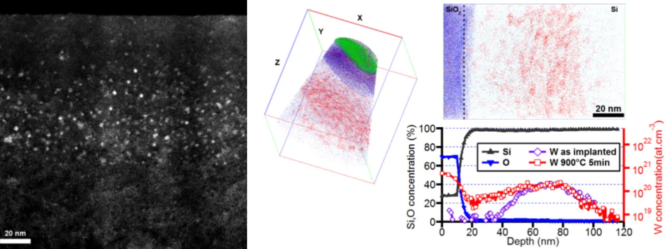
Dry oxidation of tungsten-implanted Si wafers is characterised by the formation of nanometric spherical precipitates in the Si layer (figure 5). The size and density of these precipitates versus depth follow the as-implanted W concentration profile. APT analysis of the sample oxidised at 900°C for 5 min revealed an asymmetric widening of the W profile toward the growing oxide (figure 5). It thus shows that tungsten atoms can diffuse without forming precipitates at a concentration of ~1020 at/cm3.
Figure 5. HAADF (left) and APT (right) analysis of the sample oxidised at 900°C for 5min revealed that precipitate density follows the as-implanted tungsten concentration profile. Tungsten atoms are coloured in red, oxygen in blue and nickel in green. Si atoms are not shown. The evaporated volume dimensions are 155×155×180 nm3 (X×Y×Z).
18th Microscopy of Semiconducting Materials Conference (MSM XVIII) IOP Publishing Journal of Physics: Conference Series 471 (2013) 012029 doi:10.1088/1742-6596/471/1/012029
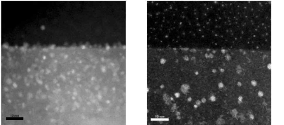
Structural analysis of precipitates revealed the coexistence of two phases: tetragonal W5Si3 and hexagonal WSi2. These precipitates exhibit topotactic relationships with the silicon matrix (topotaxy: the phenomenon of mutual orientation of two or more crystals of different species resulting from a solid-state transformation [6]). However, various precipitates’ orientations have been observed, and no predominant orientation of the precipitates has been evidenced. HAADF imaging also revealed that sub-nanometric W clusters are formed in the SiO2 layer (figure 6).
Figure 6. HAADF
comparison between
samples oxidised at 900˚C for 592 min (left) and at 1100 ˚C for 44min (right). Size evolution of precipitates in Si and clusters in SiO2 has been studied as a function of time and temperature. At 900°C, precipitates’ size increases with time whereas it doesn’t evolve notably at 1100°C, indicating that they probably reach an equilibrium state faster at higher temperature. In addition, it can be noticed that the density of clusters in the SiO2 layer seems to increase with oxidation temperature.
4. Conclusion
As expected, iron and tungsten exhibit very different behaviours during dry oxidation: iron diffuses fast and forms large β-FeSi2 precipitates at the SiO2/Si interface whereas tungsten diffusion is limited in length and brings about the formation of nanometric W5Si3 and WSi2 precipitates, with a distribution centred close to the implantation projection range. The Fe-induced pyramidal-shaped defects result from the differences in oxidation rates for iron precipitates and silicon. In both cases, iron and tungsten, oxidation of these precipitates results in the incorporation of metal into the SiO2 layer as metallic clusters.
Acknowledgement
This work has been funded by the French Ministry of Industry in the frame of the "COMET" project. (Industrial partners: ST Microelectronics, Lfoundry, Ion Beam Services, Rockwood, Biophy Research, TERA Environnement , VEGAtec)
References
[1] Graff K 2000 "Metal Impurities in Silicon Device Fabrication", Springer Series in Materials
Science, 2nd ed. (Springer, Berlin)
[2] Fujisaki Y et al 1955 J .Appl. Phys. 63, pp2304-2306 [3] Thompson K et al 2007 Ultramicroscopy 107, pp 287-298 [4] Wong-Leung J et al 1998 J. Appl. Phys 83, pp580-584 [5] Oyoshi K et al 2001 Thin Solid Films 381, pp202-208 [6] Bailey SW et al 1977 Acta Cryst. A33, pp681-684
18th Microscopy of Semiconducting Materials Conference (MSM XVIII) IOP Publishing Journal of Physics: Conference Series 471 (2013) 012029 doi:10.1088/1742-6596/471/1/012029