HAL Id: hal-01840795
https://hal.archives-ouvertes.fr/hal-01840795
Submitted on 16 Jul 2018
HAL is a multi-disciplinary open access
archive for the deposit and dissemination of
sci-entific research documents, whether they are
pub-lished or not. The documents may come from
teaching and research institutions in France or
abroad, or from public or private research centers.
L’archive ouverte pluridisciplinaire HAL, est
destinée au dépôt et à la diffusion de documents
scientifiques de niveau recherche, publiés ou non,
émanant des établissements d’enseignement et de
recherche français ou étrangers, des laboratoires
publics ou privés.
Synchronous Full-Adder based on Complementary
Resistive Switching Memory Cells
Y Zhang, Erya Deng, Jacques-Olivier Klein, Damien Querlioz, Dafiné
Ravelosona, Claude Chappert, Weisheng Zhao, Mathieu Moreau, Jean-Michel
Portal, Marc Bocquet, et al.
To cite this version:
Y Zhang, Erya Deng, Jacques-Olivier Klein, Damien Querlioz, Dafiné Ravelosona, et al..
Syn-chronous Full-Adder based on Complementary Resistive Switching Memory Cells. 11th
Interna-tional New Circuits and Systems Conference (NEWCAS), Jun 2013, Paris, France.
�10.1109/NEW-CAS.2013.6573578�. �hal-01840795�
Synchronous Full-Adder based on Complementary
Resistive Switching Memory Cells
Y. Zhang, E.Y. Deng, J.O. Klein, D. Querlioz,
D. Ravelosona, C. Chappert, W.S. Zhao*
IEF, Univ. Paris-Sud, UMR 8622, CNRS, Orsay, France
**M. Moreau, J.M. Portal, M. Bocquet, H. Aziza,
D. Deleruyelle, C. Muller
Aix-Marseille University, IM2NP – UMR CNRS 7334 Marseille, France
Abstract—Emerging non-volatile memories (NVM) such as
STT-MRAM and OxRRAM are under intense investigation by both academia and industries. They are based on resistive switching mechanisms and promise advantageous performances in terms of access speed, power consumption and endurance (i.e. >1012),
surpassing mainstream flash memories. This paper presents a non-volatile full-adder design based on complementary resistive switching memory cells and validates it through two NVM technologies: STT-MRAM and OxRRAM on 40 nm node. This architecture allows low power consumption. Thanks to the non-volatility and 3D integration of NVM, both standby power during “idle” state and data transfer power can be reduced. Using a low changing frequency can also control the switching power of NVM. The complementary cells and parallel data sensing enable fast computation and high reliability.
I. INTRODUCTION
Modern computing systems suffer from rising static power due to high leakage currents which increase exponentially with the downscaling of Complementary metal–oxide– semiconductor (CMOS) technologies [1]. According to ITRS roadmap in 2012, the static power will play a predominant role in power consumption in the coming years [2]. In order to overcome this power issue, hybrid circuits integrating resistive switching non-volatile memory (NVM) are being investigated by both academia and industries. Due to their advantageous performances, Spin Transfer Torque Magnetic Random Access Memory (STT-MRAM) [3] and Oxide Resistive RAM (OxRRAM) [4] are among the most promising NVM technologies. Indeed, as compared to conventional floating gate technologies, they provide fast write/read operations, low power consumption, CMOS compatibility and high endurance.
While these NVMs are based on different physical mechanisms, several common features exist. For instance, they consist in two terminal nanoscale devices; their resistance may be switched between ‘0’ and ‘1’ states; the memory cell may be integrated into back-end of line (BEOL) [5-8]. Recently, a number of innovative circuits based on hybrid Resistive Switching (RS) memory/CMOS circuits have been proposed. For example, magnetic look-up-table (MLUT) and non-volatile flip-flop (MFF & RS-NVFF) were introduced for reconfigurable logic circuits and normally off electronics [9-10]. A pre-charge sense amplifier (PCSA) [11] was presented and shows remarkable improvement in terms of reliability comparing with other SAs for RS memory cell sensing. In this context, resistive switching non-volatile full-adder
(RS-NVFA) based on hybrid technology could open the way towards ultra-low power and high density ICs [12]. Moreover, RS-NVFA could also overcome the communication bottleneck between separated logic module and memory block.
Magnetic Tunnel Junction (MTJ)-based RS-NVFA were proposed in the last years [13-15] and tested with conventional technology nodes. However they suffer from either high cur-rent for magnetic field generation or complex sensing circuit with capacitances. This paper presents a new full-adder design based on RS-NVM cells. Our design is validated by conducting transient simulations with two technologies: STT-MRAM and OxRRAM on 40 nm node. The rest of this paper is organized as follows: in the next section, the two technologies are briefly described and their compact models are introduced. The RS-NVFA architecture is detailed in section III. Section IV is devoted to transient simulations and performance analysis.
II. EMERGING RESISTIVE SWITCHING MEMORIES
Magnetic tunnel junction (MTJ) is the basic cell of MRAM and it consists of a thin insulating barrier (i.e. MgO) separating two ferromagnetic (FM) layers (Fig. 1a). Thanks to tunnel magneto-resistance (TMR) effect [16], its resistance, RP or RAP, depends on the relative orientation, Parallel (P) or Anti-Parallel (AP), of magnetizations in the two FM layers. STT is a switching mechanism promising high power efficiency and fast speed [2-3]. This mechanism enables profoundly simplifying CMOS circuitry, as only a bipolar current is required (Fig. 1b). MTJ switches as the passing
current exceeds a given critical current noted IC0. Recent
progresses demonstrate that perpendicular magnetic anisotropy (PMA) provides a high-energy barrier E to face the thermal instability of in-plane anisotropy. It also presents lower switching energy (<0.1 pJ/bit@32 nm) and faster speed (<1 ns) [17-19]. Si/ SiO 2 CoFeB MgO CoFeB Ta Ru Cr/Au Ta Ru Ta Al2O3 Al2O3 V-‐ V+ CoFeB MgO CoFeB P P AP AP IP -‐>AP >IC0 IAP -‐>P >IC0 CoFeB MgO CoFeB CoFeB MgO CoFeB CoFeB MgO CoFeB Free layer Reference layer (a) (b)
Figure 1. (a) Vertical structure of MTJ composed of CoFeB (1.3)/MgO (0.85)/CoFeB(2) thin films. (b) STT switching mechanism: the MTJ state changes either from P to AP as the electrons flow from the top (IP->AP>IC0), or
A CoFeB/MgO/CoFeB PMA STT-MTJ compact model [20] taking into account related static, dynamic and stochastic behaviors was used to perform transient simulation [17-18]. Table I shows the critical parameters used in the model.
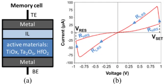
In its simplest form, an OxRRAM memory element relies on a Metal/Insulator/Metal (MIM) stack (Fig. 2a). The MIM structure is generally composed of metallic electrodes sandwiching an active layer, usually an oxygen-deficient oxide. A large number of resistive switching oxides, like
HfO2, Ta2O5, NiO, TiO2 or Cu2O, are reported in the
literature [21-23]. An interfacial layer (IL, Fig. 2a) can also appear during the fabrication process. After an initial electroforming process, the memory element may be switched reversibly between a High Resistance State (HRS or OFF state) and a Low Resistance State (LRS or ON state). In this paper, we focus on bipolar switching RS-NVM. Bipolar voltages (positive or negative) over specific threshold voltage
(i.e. VSET and VRESET) are required to switch the RS-NVM to
OFF state or ON state (Fig. 2b).
Even if OxRRAM technology is still in its “infancy”, it is broadly accepted that the field-assisted motion of oxygen vacancies plays a predominant role in bipolar resistance switching [24]. The proposed OxRRAM modeling approach, deriving from a unipolar model [25], relies on electric field-induced migration of oxygen vacancies within the switching layer. This model enables continuously accounting for both set and reset operations into a single master equation and demonstrates its flexibility to match static (switching voltages, current levels) and dynamic behaviors of the most aggressive component from literature [26-28]. Tables II summarizes the cell operation parameters for very short programming pulse used for the OxRRAM-based NVFA transient simulations.
Metal IL active materials: TiOx, Ta2O5, HfO2
Metal TE
BE Memory cell
(a) (b)
Figure 2. (a) OxRRAM memory stack with metal electrodes sandwiching an interfacial layer (IL) and an active material layer, (b) simulated
current-voltage characteristic of a bipolar OxRRAM memory cell.
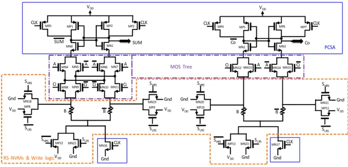
III. RESISTIVE SWITCHING FULL-ADDER ARCHITECTURE
For a 1-bit full-adder, the inputs are “A”, “B”, “Ci” and
the outputs are “SUM”, “CO”, calculated with the following
Boolean equations:
SUM = A ⊕ B ⊕ Ci= A BCi+ A B Ci+ A BCi+ A B Ci (1)
Co = A B + ACi+ BCi (2)
In the proposed architecture the input “A” is volatile computing data and input “B” is a critical data or quasi-constant. MOS transistors and RS-NVM are used to represent data “A” and “B”, respectively, in the addition. The switching
frequency of “B” is much lower than “A” and “Ci”. The
RS-NVFA architecture is composed of three parts: (i) a PCSA stage to evaluate the logic value of RS-NVFA outputs; (ii) a write logic block to program the RS memory cells; (iii) a CMOS logic tree including RS cells, implementing the addition sum and outputting carry. The general architecture is depicted in Fig. 3.
In order to evaluate the addition logic function, PCSA circuit enables providing the best sensing reliability and power efficiency while keeping high-speed performance (e.g. 200 ps) [11]. As shown in Fig. 4, it consists of pre-charge sub-circuit (MP0,3,4,7), a discharge sub-circuit (MN16-17) and a pair of
inverters (MN0-1,2-3 and MP1-2,5-6), which act as current sense
amplifier. The PCSA works in two phases: during the first phase, “CLK” is ‘0’, the RS-NVFA outputs (“SUM”, “ SUM ”
for the sum output and “CO”, “ Co ” for the carry output) are
pulled-up to “VDD” or logic ‘1’ through MP0,3,4,7 while MN16-17
remains off; during the second phase “CLK” is ‘1’, MP0,3,4,7
are turned off and MN16-17 are on. In these conditions, the
RS-NVFA outputs are pulled-down through the logic tree (MN4-15)
and the RS cells (B, B ). Depending on the MOS state in the logic tree and the RS element state, the discharge currents are different in both branches and the current sense amplifier
latches opposite logic value on “SUM”, “ SUM ” and “CO”,
“ Co ” respectively. While RS-NVFA outputs are evaluated through a differential process, the logic functions are implemented in two identical branches. However, in each branch, MOS transistors are controlled with complementary values and RS cells are programmed in opposite resistance
states (i.e. RHRS and RLRS).
The RS devices are serially connected with a common central point. In order to generate bi-directional currents to program the complementary RS cells, write logic block,
composed of pass transistors (MN18-23 and MP8-13, see Fig. 4),
is introduced. Pass transistors are connected respectively to bottom (BE) and top electrodes (TE) of the serial branch and to the common point.
Figure 3. General archtitecture of RS-NVFA composed of PCSA, CMOS tree for volatile data and non-volatile memory cells for non-volatile data.
TABLEII
CELL OPERATION PARAMETERS.
Parameter VTE (V) VBE (V) STATE
SET (Write) 0.95@5ns 0 ON->OFF
RESET (Erase) 0 -0.95V@5ns OFF->ON
Read <0.8@10ns Sensing ON or OFF
TABLEI
PARAMETERS AND VARIABLES PRESENT IN THE FITTING FUNCTIONS
Parameter Description Default Value
Area MTJ surface 40 nm x 40 nm
TMR(0) TMR ratio with 0 Vbias 120%
V Volume of free layer surface x1.3 nm
R·A Resistance-area product 10 Ωµm2
Vwrite Writing voltage 1.5 V
Vread Reading voltage 1.2 V
In such a manner, as a control signal (SLRS or SHRS) is activated,
the first RS device noted B is put in RHRS or RLRS state while
the second RS device noted B is put in the complementary
state RLRS or RHRS. Write circuitry can also serve as current
limiting transistors to prevent excess currents during the electroforming of OXRRAM devices.
It is important to note that there is no capacitance for the data sensing and no magnetic field for data programming in this new structure, compared to the previous structures [12-14]. Thereby this design is suitable for advanced technological nodes below 90 nm and allows efficient area minimization.
IV. RS-NVFAVALIDATION WITH BIPOLAR STT-MRAM
AND OXRRAMCELLS
This section presents transient simulation results to prove the architectural concept of RS-NVFA using our NVM compact models, shown in section II, and CMOS STMicroelectronics 40 nm design kit [29]. In the simulations, the size of transistors in PCSA and MOS tree is minimal while write circuit transistors are designed to reach SET and RESET states of RS cells.
Using our STT-MRAM compact model [20], we simulate the RS-NVFA architecture shown in Fig.4. Fig. 5 demonstrates the transient simulation results of the hybrid circuit. “CLK”=‘0’ drives the outputs “SUM” and “Co” to be
pre-charged to “VDD” or logic ‘1’, then the output evaluation
will occur when “CLK” is set to ‘1’. We find that the behaviors of the outputs (“SUM” and “Co”) agree with the addition function for the whole truth table. For instance, as “A”=‘1’, “B”=‘0’, “Ci”=‘0’, the result will be ‘1’ and no carry yields; in another case, “A”=‘1’, “B”=‘0’, “Ci”=‘1’, “SUM” will be ‘0’ and the carry becomes ‘1’. It is important to note that the switching duration of input “B” for STT-MRAM cell is about 2 ns [20].
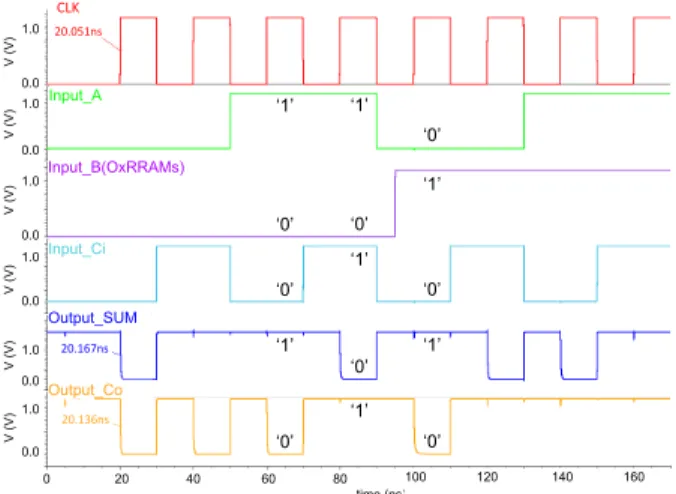
Similarly, the functionality of RS-NVFA circuit was checked through transient simulations with OxRRAM cells and CMOS STMicroelectronics 40 nm design kit [29] (Fig. 6). For OXRRAM cells, the switching time depends on write voltage dynamics. The simulation results obtained with our model [27] give a switching time less than 3 ns and resistance
values RHRS=35.1kΩ and RLRS=1.1kΩ. The outputs “SUM”
and “Co” confirm the whole full-adder function. The sense delay is less than 60 ps for both outputs, showing high-speed performance of OxRRAM-based NVFA.
We summarize the performance comparison between three different simulations in Table III. The delay time and dynamic power of RS-NVFAs (with STT-MRAM and OxRRAM cells) are comparable to CMOS FA coming from standard cell library of STMicroelectronics [29]. It is advantageous in terms of standby power since our design allows to be powered off completely during “idle” state. Although its energy-delay product (EDP) exceeds that of CMOS full-adder by ~30%, then RS-NVFA could greatly reduce the whole consumption. Thanks to the 3D integration, the die area of our design (38 MOS + 4 RS cells) is more compact than the CMOS Full-adder (46 CMOS: 28 CMOS for asynchronous full-Full-adder + 18 CMOS for synchronization) as the RS memories are on top of CMOS circuits. This integration allows also the elimination of dynamic power dedicated for data transfer (1 pJ/mm/bit@22 nm [2,30]) between logic units and memory array as the distance between memory and computing unit becomes some µm instead of some mm for CMOS logic circuits [30].
Figure 5. Transient simulations of RS-NVFA with STT-MRAM cells. Outputs are pre-charged as CLK is set to ‘0’ and are evaluated as CLK is set
to ‘1’. CLK MP0 CLK MP1 MP2 MP3 MN0 MN1 SUM SUM MN4 MN5 MN6 MN7 MN8 MN9 MN10 MN11
A A A A
Ci Ci Ci Ci
B B MN22 MP12 VDD VDD Gnd Gnd MN16 SHRS SLRS CLK VDD Gnd MN18 MP8 SLRS SHRS VDD Gnd MN19 MP9 SLRS SHRS CLK MP4 CLK MP5 MP6 MP7 MN2 MN3 Co Co MN12 MN13 MN14 MN15
Ci A A
B B MN23 MP13 VDD VDD Gnd Gnd MN17 SHRS SLRS CLK VDD Gnd MN20 MP10 SLRS SHRS VDD Gnd MN21 MP11 SLRS SHRS v PCSA
RS-‐NVMs & Write logic
Ci
MOS Tree
Figure 4. Resistive switching non-volatile full-adder architecture with SUM signal (left) and output carry CO (right) sub-circuit.
‘1’ ‘0’ ‘0’ ‘1’ ‘0’ ‘1’ ‘0’ ‘1’ ‘0’ ‘1’ ‘0’ ‘1’ ‘0’ ‘1’ ‘0’ CLK$ Input_B(OxRRAMs) Input_Ci 1.0 0.0 1.0 0.0 1.0 0.0 1.0 0.0 1.0 0.0 1.0 0.0 V (V) V (V) V (V) V (V) V (V) V (V) Input_A Output_SUM Output_Co 20.051ns$ 20.167ns$ 20.136ns$ 0 20 40 60 80 100 120 140 160 180 time (ns) ‘1’ ‘0’ ‘0’ ‘1’ ‘0’ ‘1’ ‘0’ ‘1’ ‘0’ ‘1’ ‘0’ ‘1’ ‘0’ ‘1’ ‘0’ CLK$ Input_B(OxRRAMs) Input_Ci 1.0 0.0 1.0 0.0 1.0 0.0 1.0 0.0 1.0 0.0 1.0 0.0 V (V) V (V) V (V) V (V) V (V) V (V) Input_A Output_SUM Output_Co 20.051ns$ 20.167ns$ 20.136ns$ 0 20 40 60 80 100 120 140 160 time (ns)
Figure 6. Transient simulations of RS-NVFA with OxRRAM cells. The simulation conditions are identical to those used in Fig. 5.
As mentioned above, a critical idea of this design shown in Fig. 4 is to use a programming frequency (e.g. 1 KHz) of RS-NVM much lower than the computing frequency (e.g. 1 GHz). Thereby, the switching power for non-volatile storage becomes insignificant to other power consumption in a full system.
V. CONCLUDING REMARKS
This paper presents a generic design of RS-NVFA based on complementary RS memory cells. Our RS-NVFA circuit is suitable for advanced technological nodes as there is neither capacitance nor magnetic fields compared to previous structures [11-15]. This architecture enables scaling down the die area and reducing the power as there is nearly zero standby power and low data transfer energy. It can be very useful for normally off electronics [19]. Using our STT-MRAM and OxRRAM compact models, RS-NVFAs were successfully simulated on 40 nm node and demonstrated their functionality and performance gain.
ACKNOWLEDGMENT
The authors acknowledge support from French research agencies through projects NANOINNOV-SPIN, CNRS-PEPS-NVCPU, ANR-MARS and ANR-DIPMEM.
REFERENCES
[1] N.S. Kim et al., “Leakage current: Moore's law meets the static power”, Computer, vol. 36, pp. 68-75, 2003.
[2] International Roadmap for semiconductor (ITRS), 2012 ERD Update.
[3] C. Chappert, A. Fert and F. Nguyen Van Dau, “The emergence of spin electronics in data storage”, Nat. Mater., vol. 6, pp. 813-823, 2007. [4] I.G. Baek et al., “Multi-layer cross-point binary oxide resistive memory
(OxRRAM) for post-NAND storage application”, IEDM Tech. Dig., pp. 750-753, 2005.
[5] C.J. Lin et al., “45nm Low power CMOS logic compatible embedded STT MRAM utilizing a reverse-connection 1T/1MTJ cell”, IEDM Tech. Dig., pp. 279-282, 2009.
[6] K. Tsuchida et al., “A 64Mb MRAM with clamped-reference and adequate-reference schemes”, IEEE Proc. of ISSCC, pp. 258-259, 2010.
[7] W.S. Zhao, E. Belhaire, C. Chappert, and P. Mazoyer, “Spin Transfer Torque (STT)-MRAM based Run Time Reconfiguration FPGA circuit”, ACM Trans. Embedded Computing Systems, vol. 9, no. 2, art. 14, 2009.
[8] S. Chung et al., “Fully integrated 54nm STT-RAM with the smallest bit cell dimension”, IEDM Tech. Dig., pp. 304-307, 2010.
[9] W.S. Zhao et al., “New non-volatile logic based on spin-MTJ”, Physica Status Solidi-A, vol. 6, pp. 1373-1377, 2008.
[10] S. Onkaraiah et al., “Bipolar ReRAM based non-volatile flip-flops for low-power architectures”, IEEE Proc. of NEWCAS, pp. 417-420, 2012. [11] W.S. Zhao, C. Chappert, V. Javerliac, and J.-P. Noziere, “High speed, high stability and low power sensing amplifier for MTJ/CMOS hybrid logic circuits”, IEEE Trans. Magn., vol. 45, pp. 3784-3787, 2009. [12] S. Matsunaga et al., “Fabrication of a nonvolatile full adder based on
logic-in-memory architecture using magnetic tunnel junctions,” Appl. Phys. Express, vol. 1, no. 9, p. 091301, 2008.
[13] Y. Gang, et al., “A high-reliability, low-power magnetic full adder”, IEEE Trans. Magn., vol. 47, no. 11, pp. 4611–4616, 2011.
[14] F. Ren and D. Markovic, “True energy-performance analysis of the MTJ-based logic-in-memory architecture (1-bit full adder),” IEEE Trans. Electron Devices, vol. 57, no. 5, pp. 1023–1028, 2010.
[15] S. Lee, S. Seo, S. Lee, and H. Shin, “A full adder design using serially connected single-layer magnetic tunnel junction elements,” IEEE Trans. Electron Devices, vol. 55, no. 3, pp. 890–895, 2008.
[16] M. Julliere, “Tunneling between ferromagnetic films”, Physics Letters A, vol. 54, pp. 225-226, 1975.
[17] S. Ikeda et al., “A perpendicular-anisotropy CoFeB–MgO magnetic tunnel junction”, Nat. Mater., vol. 9, pp. 721-724, 2010.
[18] D. C. Worledge et al., “Spin torque switching of perpendicular Ta|CoFeB|MgO-based magnetic tunnel junctions”, Appl. Phys. Lett., vol. 98, p. 022501, 2011.
[19] H. Yoda et al., “Progress of STT-MRAM technology and the effect on Normally-Off computing systems”, IEDM Tech. Dig., pp. 11.3.1-11.3.4, 2012.
[20] Y. Zhang et al., “Compact modeling of perpendicular-anisotropy CoFeB/MgO magnetic tunnel junctions”, IEEE Trans. Electron Devices, vol. 59, no. 3, pp. 819-826, 2012.
[21] R. Waser and M. Aono, “Nanoionics-based resistive switching memories”, Nat. Mater., vol. 6, pp. 833-840, 2007.
[22] S. Seo et al., “Reproducible resistance switching in polycrystalline NiO films”, Appl. Phys. Lett., vol. 85, pp. 5655-5657, 2004.
[23] W.G. Kim et al., “Dependence of the switching characteristics of resistance random access memory on the type of transition metal oxide”, IEEE Proc. of ESSDERC, pp. 400-403, 2010.
[24] H.S. Ahn, S. Han, and C.S. Hwang, “Pairing of cation vacancies and gap-state creation in TiO2 and HfO2”, Appl. Phys. Lett., vol. 90, p. 252908, 2007.
[25] M. Bocquet, D. Deleruyelle, C. Muller, J.-M. Portal, “Self-consistent physical modeling of set/reset operations in unipolar resistive-switching memories”, Appl. Phys. Lett., vol. 98, no. 26, pp. 263507(1–3), 2011. [26] C. Cagli et al., “Experimental and Theoretical Study of Electrode
Effects in HfO2 based RRAM”, IEDM Tech. Dig., pp. 28.7.1-28.7.4, 2011.
[27] H. Aziza, M. Bocquet, J.-M. Portal and C. Muller, “Evaluation of OxRAM Cell Variability Impact on Memory Performances through Electrical Simulations”, IEEE Proc of Non-Volatile Memory Technology Symposium (NVMTS), pp. 1-5, 2011.
[28] H. Aziza, M. Bocquet, J-M. Portal and C. Muller, “Bipolar OxRRAM memory array reliability evaluation based on fault injection”, IEEE Proc. Of Design and Test Workshop (IDT), pp. 78-81, 2011.
[29] STMicroelectronics, Manuel of design kit for CMOS 40nm, 2012. [30] M. Duranton, “New computing architectures for Green ICT”, Chist-era
conference, 2011.
TABLEIII
COMPARISON OF 1-BIT RS-NVFA WITH CMOS-ONLY FA @40 nm Performance
CMOS-ONLY
FA
STT-MRAM
NVFA OxRRAM NVFA
Delay time 75 ps 87.4 ps 52.3 ps Dynamic power@ 500 MHz 2.17 uW 2.44 uW 3.50 uW Standby power 71 nW ~0 ~0 Data transfer energy >1 pJ < 1fJ < 1fJ