HAL Id: hal-00794987
https://hal.archives-ouvertes.fr/hal-00794987
Submitted on 26 Feb 2013
HAL is a multi-disciplinary open access archive for the deposit and dissemination of sci-entific research documents, whether they are pub-lished or not. The documents may come from teaching and research institutions in France or abroad, or from public or private research centers.
L’archive ouverte pluridisciplinaire HAL, est destinée au dépôt et à la diffusion de documents scientifiques de niveau recherche, publiés ou non, émanant des établissements d’enseignement et de recherche français ou étrangers, des laboratoires publics ou privés.
Organisation of carbon nanotubes and semiconductor
nanowires using lateral alumina templates
Didier Pribat, Costel Sorin Cojocaru, M. Gowtham, B. Marquardt, T. Wade,
Jean Eric Wegrowe, B.S. Kim
To cite this version:
Didier Pribat, Costel Sorin Cojocaru, M. Gowtham, B. Marquardt, T. Wade, et al.. Organisation of carbon nanotubes and semiconductor nanowires using lateral alumina templates. Comptes Rendus Physique, Centre Mersenne, 2009, 10 (4), pp.320–329. �10.1016/j.crhy.2009.05.007�. �hal-00794987�
C. R. Physique
vol. 10 (2009) 320–329
DOI: http://dx.doi.org/10.1016/j.crhy.2009.05.007
Carbon nanotube electronics / Électronique à nanotubes de carbone
Organisation of carbon nanotubes and semiconductor nanowires
using lateral alumina templates
D. Pribat
a,∗, C.S. Cojocaru
a, M. Gowtham
a, B. Marquardt
a, T. Wade
b,∗, J.E. Wegrowe
b,
B.S. Kim
c
a Laboratoire de physique des interfaces et des couches minces (LPICM), École polytechnique, 91128 Palaiseau cedex, France b Laboratoire des solides irradiés (LSI), École polytechnique, 91128 Palaiseau cedex, France
c Samsung Electronics, Giheung-Gu, Yongin-City, Gyeonggi-Do, Republic of Korea 446-711
Abstract
Carbon nanotubes and semiconductor nanowires have been thoroughly studied for the future replacement of silicon-based com- plementary metal oxide semiconductor (CMOS) devices and circuits. However, the organisation of these nanomaterials in dense transistor arrays, where each device is capable of delivering drive currents comparable with those of their silicon counterparts is still a big challenge. Here, we present a novel approach to the organisation of carbon nanotubes and semiconductor nanowires, based on the use of porous lateral alumina templates obtained by the controlled anodic oxidation of aluminium thin films. We discuss the growth of nanomaterials inside the pores of such templates and show the feasibility of our approach. Our first results point to further work on controlling the synthesis of catalyst nanoparticles at the bottom of the pores, these particles being necessary to nucleate and sustain the growth of carbon nanotubes or semiconductor nanowires.
.
Résumé
Organisation de nanotubes de carbones et de nanofils semiconducteurs en utilisant une membrane latérale en alumine nanoporeuse. Depuis quelques années, les nanotubes de carbone et les nanofils semiconducteurs sont étudiés pour le remplacement
des composants CMOS à base de silicium. Des caractéristiques de transistors à effet de champ impressionnantes ont été obtenues en utilisant ces nanomatériaux. Le problème toutefois est d’organiser les nanotubes et les nanofils en réseaux de transistors avec des densités comparables à celles de leurs homologues en silicium. Nous présentons ici une approche nouvelle, dans laquelle les nanotubes et les nanofils sont organisés par croissance dans des membranes latérales nanoporeuses obtenues par oxydation anodique de films minces d’aluminium. Nous discutons la croissance des nanotubes et des nanofils dans les pores et démontrons la faisabilité de l’approche proposée. Nos premiers résultats indiquent que le contrôle du dépôt, au fond des pores, des nanoparticules catalytiques nécessaires à la nucléation et à la croissance des nanotubes et des nanofils est essentiel pour permettre l’obtention de réseaux denses et organisés, compatibles avec les standards de la microélectronique.
Keywords: Carbon nanotubes; Silicon nanowires; Device applications; Controlled growth and organisation; Templates; Porous anodic alumina
1. Introduction and context
As the scaling down of the silicon metal oxide (MOS) transistor is reaching physical limitations, researchers are concentrating on finding new materials or paradigms that could enable the semiconductor industry to continue fol- lowing the pace of Moore’s law. Within this context, single wall carbon nanotubes (SWNTs) have been thoroughly investigated over the past few years and devices based on individual specimens have shown breathtaking characteris- tics [1]. Semiconductor nanowires (s-NWs) are another class of nanomaterials also studied within the frame of MOS replacement [2].
However, when dealing with MOS replacement, one must be well aware of the magnitude of the challenge. The microelectronics industry has produced an incredible and unprecedented level of organisation, where more than 109 transistors are crammed onto ~ one cm2 of a silicon substrate [3], each individual device exhibiting a lithography- controlled gate length of ~ 30 nm (corresponding to the so-called 32 nm node). This spectacular miniaturisation has been made possible by constant progress in photolithography and micromachining (top-down approach), a paradigm that applies well to bulk or thin-film type “continuous” materials.
Actually, carbon nanotubes represent a new type of nanomaterial that does not exist in traditional bulk form. The same holds for semiconductor nanowires. Random carbon nanotube networks [4] are the “thin-film” equivalent form of CNTs. Although devices made from such films exhibit stunning characteristics [5] (especially considering their relatively simple processing conditions), such characteristics (carrier mobility, subthreshold slope, . . .) are still degraded compared to those of counterpart devices obtained with individual SWNT specimens (compare device results from Ref. [1] with those of Ref. [5]). Also, such random films are not amenable to ultra large scale integration (ULSI)- type manufacturing methods because they are not continuous at the nanometric scale. Hence, new paradigms and fabrication schemes have to be found, in order to allow the use of such nano-materials (or rather collections of such nano-objects) and be able to compete with the organisation and complexity levels reached by silicon MOS technology.
The problem now is to find means to organise SWNTs and s-NWs in dense arrays that will allow device densities comparable to those of ULSI circuits. For instance, the current-carrying capability of a well engineered (strained) Si MOS transistor is around 1 mA/µm of gate width.1 On the other hand, a carbon nanotube field-effect transistor (CNTFET) built with an individual semiconductor SWNT specimen will deliver several µA of on-current [1] (say 10 µA/tube for the sake of being quantitative [6]). On this basis, by using a scaling law that takes into account a partial screening of the gate field as SWNTs are brought closer, drive currents well over 2 mA/µm of gate width can be calculated for CNTFETs based on parallel organised, compact arrays of SWNTs [7,8]. Thus CNTFETs are
potentially capable of much higher drive currents per unit width than Si MOSFETs.
The problem, however, is that so-far, no one has been able to organise SWNTs in dense enough arrays, exhibit- ing several hundreds SWNTs (~ 700 for a 1.4 nm diameter) per µm and capable of delivering currents well over 2 mA/µm. Many techniques of organisation have been studied, whether put in practice during SWNT growth [9] or following their solubilisation in liquid suspensions [10]. However, to the best of our knowledge, the highest in-plane SWNT density reported so far is around 50 µm1 [11], obtained by direct growth on (ST cut) quartz surfaces and this density is far from being homogeneous, which seems to preclude any scaling of the method over large areas and large device quantities. The most recent papers present drive currents of 20 µA/µm of gate width for CNTFET devices and circuits [12], far below the extrapolated values of Refs. [7] and [8].
For s-NWs, the best reported in-plane densities are even smaller, below 10 µm1 [13]. With such NW densities, it takes about 100 µm of gate width for a transistor to reach a drive current of ~ 1 mA (i.e., 100 times larger than the corresponding bulk Si MOSFET, see Fig. 5(b) of Ref. [13]).
In this article, we present a novel approach to the organisation of SWNTs or semiconductor NWs, based on the use of template structures. Such templates can yield very dense assemblies of nano-objects as will be detailed below.
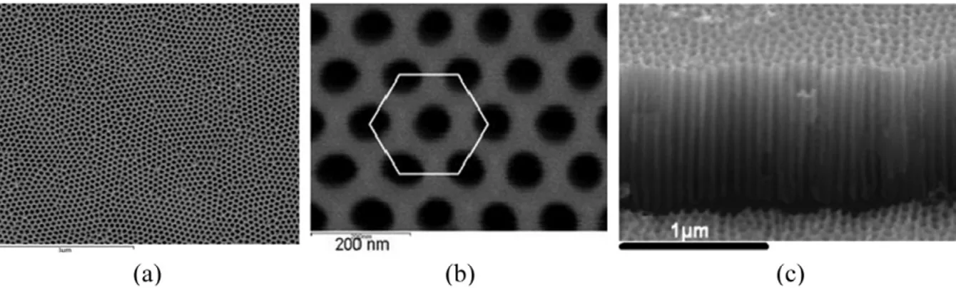
Fig. 1. Scanning electron microscope (SEM) pictures of porous anodic alumina membranes obtained by anodic oxidation of Al substrates in oxalic acid at 55 V. (a): Top view of a large portion of the membrane. (b): Detail of the membrane showing ~ 70 nm diameter pores. Note the quality of the self-ordering highlighted by the white hexagon. Smaller pores (down to ~ 5 nm) can be obtained in sulphuric acid electrolytes and at a lower anodic voltage. (c): Cross section of the membrane showing straight and parallel-aligned pores (~ 1 µm long).
1 At the 2008 IEDM conference (15–17 December), Intel announced 1.55 mA/µm for NMOS and 1.21 mA/µm for PMOS transisors, using their
2. Porous anodic alumina templates
In recent years, various templates have been used for the organisation of nano-objects such as nanowires (metallic or semiconducting) or carbon nanotubes (see Ref. [14] for a recent review). The most widespread templates are ion track-etched membranes and porous anodic alumina membranes. Ion-track etched membranes are usually synthesized by high energy ion irradiation of polycarbonate films coated on a conducting substrate [15]. Because of the irradiation process, the pores are randomly organised. Moreover, being made of polycarbonate, such membranes are not refractory and cannot withstand a high temperature treatment such as the growth of SWNTs or s-NWs by chemical vapour deposition (see below).
On the other hand, porous alumina membranes (PAA) are synthesised by anodic oxidation of aluminium films/substrates at room temperature. Anodic oxidation is an electrochemical process by which aluminium is trans- formed into its oxide at the anode of an electrochemical cell. Under certain oxidation conditions (i.e., when the resulting alumina is soluble in the electrolyte), the alumina film turns out to be porous (instead of continuous) and the pores can be self-organised into a hexagonal structure [16–18]. The electric field-assisted oxide dissolution, together with the oxide volume expansion of ~ 1.2 (that generates an interface stress) are at the origin of pore nucleation. Pore growth is the result of an equilibrium process between oxide dissolution at the interface with the electrolyte and oxide formation. A two step anodic oxidation process yields highly self-ordered, honeycomb-like hexagonal pore arrays, with a circular pore at the centre of each hexagon [17].
The pore diameter, Φp , and the inter-pore distance, Dint , are proportional to the anodization voltage U . Actually,
Φp = k1 U and Dint = k2 U , where k1 ~ 1.29 nm/V and k2 ~ 2.5 nm/V at room temperature [18]. For low anodization
voltages (e.g., 2–3 V) in sulphuric acid electrolytes, high pore densities can be obtained, of the order of several 1012 cm2 , corresponding to more than 100 µm1 on a linear scale.
As an illustration, Fig. 1 shows scanning electron microscope (SEM) pictures of PAA membranes synthesised in our group. Note the high degree of in-plane self-organisation (Fig. 1(a)) and the rectitude of the pores (Fig. 1(b)).
Carbon nanotubes [19] (including SWNTs [20]) as well as silicon NWs [21] have been grown inside alumina templates by the so-called vapour–liquid–solid (VLS) mechanism [22]. In the VLS mechanism, a metal (or rather a nanoparticle of a metal [23] in the present context) forming a low temperature eutectic alloy with either silicon [22,23] or carbon [24] is used as a catalyst for growing carbon nanotubes (CNTs) or s-NWs from gaseous precursors such as CH4 , C2 H2 or SiH4 . When the VLS-type synthesis mechanism is activated, the final diameter of the NW or CNT is
controlled by the critical dimension (diameter) of the metallic nanoparticles (e.g., Au for Si growth, see Ref. [23], and Fe for CNT growth, see Ref. [24]). Such metallic nanoparticles can originate from colloidal solutions [23,25] or be prepared in situ, from thin-film fragmentation upon annealing [26]. In any case, clustering and agglomeration of the nanoparticles must be prevented, if a uniform diameter distribution of NWs or CNTs is to be obtained after growth. The advantage of using PAA templates is that catalyst nanoparticles can be electrodeposited at the bottom of the pores of the membrane (after its synthesis) and their possible diffusion (upon exposure to high temperature, e.g., during growth) and agglomeration (by e.g., an Ostwald ripening mechanism [27]) blocked. Moreover, as the pore diameter distribution is usually very uniform and monodispersed, nano-objects with controlled diameters can be obtained [21].
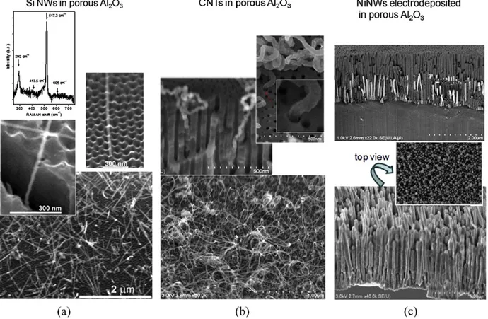
Again as an illustration, Fig. 2 shows Si NWs, CNTs and Ni nanowires grown in our laboratory inside vertical PAA membranes. The Ni nanowires were simply grown by electrodeposition, whereas the Si NWs and CNTs were grown by VLS in a chemical vapour deposition (CVD) reactor using H2 -diluted SiH4 and C2 H2 respectively as growth
nutrients. Prior to CVD-VLS growth, Cu (for Si NW growth) or Ni or Co (for CNT growth) catalyst particles were electrodeposited at the bottom of the pores of the membranes. The Si NWs were grown at 500–550 ◦C and the CNTs were grown at 600–620 ◦C. In order to get a uniform catalyst or Ni NW deposition, a special membrane preparation technique is systematically applied, by which the anodization current is decreased according to an exponential law (as a function of time) at the end of the anodic oxidation step [28]. Finally, we note that the CNTs are not single walled, because the pore diameter (and hence the diameter of the Ni or Co catalyst particles) was too large in those samples. SWNTs can be grown in vertical PAA templates by using special tricks to get catalyst particles in the nanometer range (see Ref. [20]).
Fig. 2. Various nanostructures grown inside vertical porous anodic alumina templates. (a): Different SEM views of Si NWs grown from electrode- posited Cu catalysts. From bottom to top: (i) surface of the membrane after VLS growth; for easy observation, the growth time has been purposely made longer, which results in NWs growing out of the membrane, (ii) detail of a NW emerging from a pore, (iii) the membrane has been broken in order to check that NW nucleation occurred at the bottom of the pores, where the Cu nanoparticles are electrodeposited, (iv) Raman spectrum of the nanowires evidencing their good crystalline quality. (b): Different views of CNTs grown from electrodeposited Ni catalysts. From bottom to top: (i) surface of the membrane after VLS growth, (ii) cross section of a membrane showing CNTs inside it, (iii) details of CNTs emerging from the membrane, with a close view on one CNT in inset (~ 40 nm diameter). (c): Ni NWs grown by electrodeposition from a mixture of NiSO4 , NiCl2 and H3 BO3 (Watts bath). The membrane has been selectively etched in the bottom picture, in order to reveal the Ni NWs which were originally
inside the pores.
3. Lateral alumina templates
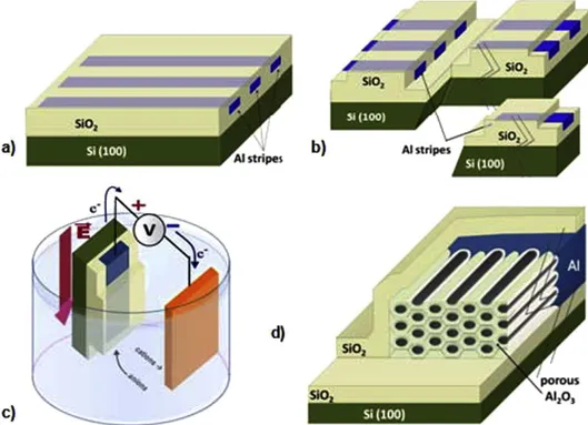
Another advantage of PAA membranes is that they can be shaped with their pores parallel to the surface of the substrate [29,30]. This can be done by engineering the anodization process of an Al thin film in such a way that the current will flow parallel to the surface of the substrate instead of perpendicular as usually done. Actually, because of the mechanism of their formation, one has to realise that the pores develop parallel to the local electric field lines and their orientation follows the flow of the anodization current inside the Al thin film [31]. So, in principle, any pore direction can be obtained, as long as the current can be channelled accordingly. Briefly, PAA lateral structures can be synthesized by using an insulating substrate (e.g., an oxidised Si wafer) and by capping stripes of a deposited Al thin film with an insulating layer (SiO2 , Si3 N4 , . . .) before anodic oxidation, thus forcing the anodization current to flow
Fig. 3. Principle of the method developed for synthesising lateral porous alumina templates. (a): Al stripes deposited on an oxidised Si wafer are caped with an insulating layer (e.g., SiO2 ). (b): The capped Al stripes are made individual by photolithography and cleavage of the substrate.
(c): Anodic oxidation of the tip of an individual Al stripe. (d): Schematic structure of the lateral porous alumina membrane at the tip of the Al stripe, after anodic oxidation.
After electrodeposition of a catalyst material at the bottom of the pores (in the same way as for vertical pores), such lateral PAA structures can be used as templates for the “planar” growth of NWs and CNTs by the VLS method, again just like in vertical templates. The result is a composite material (see Fig. 4) where nano-objects are packed with a pre- defined density, corresponding to the pore density (which is adjustable, depending on the anodization voltage and the type of electrolyte) and assuming that each pore is filled. Once growth is performed, and the nano-objects lay in-plane inside the pores, it is quite easy to deposit various metal electrodes in order to build a planar-type, three-terminal de- vice. In fact, the lateral membrane with the nano-objects inside can be shaped and micro-machined by microelectronic- type technologies (photolithography and etching) just like any other thin film and there is no need to manipulate individual nanotubes or nanowires to build electronic devices. Moreover, as quoted above, linear densities of pores larger than 100 µm1 can be obtained (corresponding to an identical potential density of NWs or CNTs), which, as far as the organisation of nano-objects is concerned, represents an advantage over the various methods developed so far.
Fig. 5 shows various examples of lateral membranes grown in oxalic acid, using Si3 N4 capping layers. In our
operating conditions, where the anodic voltage is around 50 V and the electrolytic bath is maintained at 0 ◦C, the anodization rate in oxalic acid is ~ 45 nm/minute. Although difficult to appreciate at the actual magnification of the pictures in Fig. 5, the typical pore diameter is around 50 nm. For the sake of picture clarity, we have removed the capping Si3 N4 layer (by reactive ion etching) as well as the remaining Al electrode at the back of the membrane (by
wet chemistry in a HgCl2 solution) before loading the samples in the SEM. We also point out that the thickness of the
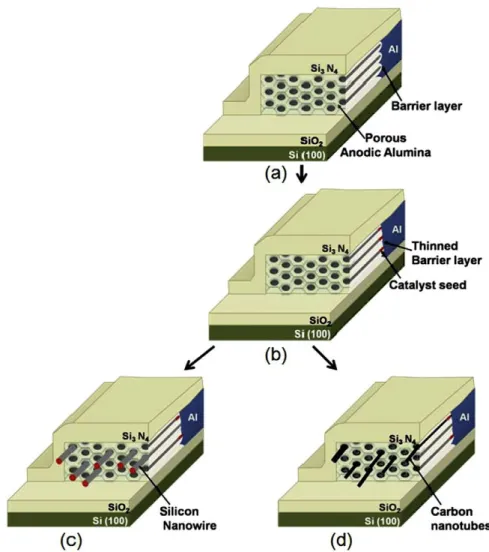
Fig. 4. Schematic principle of the growth of Si-NWs and CNTs inside porous lateral alumina membranes. (a): Schematics of the lateral membrane after synthesis. (b): After electrodeposition of catalysts at the bottom of the pores. (c): After growth of Si NWs. (d): After growth of CNTs.
After synthesis of the lateral membranes to the desired width, catalysts are electrodeposited at the bottom of the pores. For the experiments presented below, we have used CuSO4 (for Si NW growth) and CoSO4 (for CNT growth)
electrolytes, buffered with H3 BO3 (pH ~ 3.8). The electrodeposition configuration used in these experiments is a
classical 3-electrode type already reported elsewhere [32].
After the electrodeposition of the catalysts at the bottom of the pores, the samples are loaded in a CVD reactor and heated to 550 ◦C under a H2 atmosphere (typically 15 mbar) for 15 min, in order to stabilise the membranes with the
catalyst particles inside them.
For the growth of SiNWs, as quoted above, we have used a mixture of SiH4 (2.5 sccm) and H2 (97.5 sccm) at a
pressure of 10 mbar and at a temperature of 550 ◦C. However, when dealing with lateral membranes, one has to realise that the catalyst surface exposed to the growth nutrients is very small, much smaller than in the situation concerning vertical membranes, where the whole top surface of the sample is exposed. As a consequence, and because of the high supersaturation of the vapour phase, SiH4 tends to decompose on any surface, even those with a poor catalytic
activity. Hence, in order to avoid the parasitic deposition of amorphous or ill-crystallized Si on the membrane itself (which leads to a rapid clogging of the pores, thus halting NW growth), the hydrogen dilution gas was passed through a tungsten filament positioned inside the CVD tube, ~ 15 cm upstream of the sample holder. The W filament was heated to ~ 1800 ◦C (as measured with an optical pyrometer), in order to partially decompose H2 into atomic hydrogen (H·).
The temperature of the sample holder was monitored with an independent thermocouple, in order to take into account any possible additional heating effect originating from the W filament.
Fig. 5. SEM pictures of lateral membranes grown in oxalic acid. On the top picture, the membrane is ~ 1 µm wide, corresponding to a 22 minutes oxidation time whereas on the bottom picture it is ~ 250 nm wide corresponding to a 5 minutes oxidation time. The capping layer has been removed by reactive ion etching (RIE) and the remaining Al film at the back of the membranes has also been removed by selective etching in HgCl2 . The
small pillars observed on the bottom picture are defects left after RIE of the Si3 N4 cap.
Actually, H· is well known as a scavenger that preferentially etches amorphous Si. This is the reason why H· is extensively used for the growth of nano- or micro-crystalline Si by plasma enhanced CVD at low temperature [33]. The growth time for the Si NWs was typically set to 10 minutes.
For the growth of CNTs, the temperature was set to 620 ◦C and we have used a mixture of C2 H2 (30 sccm) and
H2 O (10 sccm) at a pressure of 10 mbar. Here, H2 O is used instead of H· for removing amorphous carbon [34,35].
The typical growth time was 15 min.
Fig. 6 shows various SEM pictures of Si NWs emerging from lateral membranes after CVD growth. The effect of H· is clearly seen on the pictures of Fig. 6 (b) and (c). When the W filament is not switched-on (Fig. 6(b)), parasitic Si deposition is observed all over the side wall of the membrane, which tends to block most pores, thus preventing further NW growth. We note that even when H· is used, all the pores are not filled with NWs (Fig. 6 (a) and (c)), despite us taking care to optimize the voltage decrease after synthesis of the membrane [28]. We also note that the NW diameters
Fig. 6. Various SEM pictures of Si NWs grown in porous lateral templates. (a): View of a membrane after growth with H·. The NWs are clearly seen emerging from some of the pores. (b): Another membrane after growth without H· (the W filament was not turned on); the red arrows point to those pores blocked by amorphous Si deposition and the brown one to an emerging NW. (c): Close up of the picture shown in (a). The red and brown arrows have the same meaning as in (b); the blue arrows indicate partially filled or empty pores.
Fig. 7. Various SEM pictures of CNTs grown in porous lateral templates. (a): The membrane is totally masked by CNTs protruding out of it. (b): Different electrodeposition conditions for the Co catalysts: fewer CNTs are produced (see text). (c): Details of CNTs emerging from pores. (d): Some catalysts have fragmented into smaller clusters, yielding several CNTs in one pore. Note the “cleanliness” of the side wall of the membrane, with absolutely no trace of amorphous carbon (H2 O effect).
(~ 20 nm) are smaller than those of the pores they originate from. We suspect that some of the electrodeposited copper has alloyed with Al at the bottom of the pores just before growth (during the thermal stabilization treatment), resulting in either a poisoning (no NW in the pore) or a decrease of the catalyst volume available for growth (smaller NW diameter). This problem will be solved in the future, by carefully adjusting the conditions of the exponential voltage decrease after anodization [28], in order to leave a thin alumina film at the bottom of the pores, which will isolate the catalysts from the Al electrode, acting as a diffusion barrier.
Finally, Fig. 7 shows SEM pictures of CNTs emerging from lateral membranes. Different electrodeposition condi- tions have been used for the Co catalysts. In Fig. 7(a), electrodeposition was performed with electric pulses having a 6 V amplitude, at 100 Hz frequency and during 60 s, whereas in Fig. 7(b), the deposition time was only 15 s. So the length of the catalyst particles inside the pores was smaller in the later case. As with Si NWs, the shorter Co catalysts have probably been poisoned by the remaining Al at the bottom of the pores, leading to fewer CNTs being grown.
Fig. 7 (c) and (d) display details of CNTs emerging from the inside of some pores. In particular, catalyst fragmentation seems to occur in some places, leading to the growth of several CNTs inside the same pore (Fig. 7(d)), a situation never observed for Si NWs. Here again, the CNTs are certainly not single walled (even when fragmentation of the catalyst occurs), since the pore diameter was too large to yield catalysts with diameters around 1 nm. We are currently studying a different way to introduce the catalysts, compatible with the obtainment of nm-sized clusters [36]. We also point out that the membrane’s side wall is devoid of any parasitic amorphous carbon deposition, thanks to the scavenging effect of H2 O during growth.
4. Conclusions
We have presented some early results concerning a novel way of organising nano-objects such as semiconductor nanowires and carbon nanotubes, based on the use of lateral porous alumina templates synthesized from thin films of aluminium deposited on insulating substrates. Such templates can be tailored with predefined geometrical charac- teristics (including the pore and the interpore distance down to a few nm), by carefully controlling the thickness of the Al thin film and the anodization conditions (type of electrolyte, anodizing voltage, . . . ). These templates provide a planar-type organisation well adapted to 3-terminal devices and totally compatible with existing tools inherited from advanced microelectronic processes. Pore densities over 100 µm1 can be obtained, corresponding to an equal density of NWs or CNTs, assuming a 100% filling rate. Work is now in progress in order to stabilize the NW or CNT growth processes inside the pores and increase the filling rate. In particular, special attention will be devoted, in the near fu- ture, to the catalyst deposition process, in order to avoid its poisoning by intermixing with Al. Finally, we would like to point out that lateral membranes would also simplify the fabrication process of thin film transistors used in active matrix backplanes for addressing flat panel displays. In particular, only 4 masks would be needed for the fabrication of an active matrix liquid crystal display backplane [37], a mask number competitive with that of the current amorphous silicon technology.
Acknowledgements
This work was partially funded by the NanodiX Chair with Samsung Electronics, the CANDICE EC (FP 6) project and the French ANR project NANOBIOSENSOR.
References
[1] For recent reviews on CNT-based devices, see e.g., H. Dai, A. Javey, E. Pop, D. Mann, W. Kim, Y. Lu, Nano 1 (2006) 1–13, and references therein;
Ph. Avouris, J. Chen, Mater. Today 9 (October 2006) 46–54.
[2] See e.g., “Emerging Research Devices” in the 2007 International Technology Roadmap for Semiconductors, http://www.itrs.net/Links/ 2007ITRS/2007_Chapters/2007_ERD.pdf.
[3] See: http://www.intel.com/technology/architecture-silicon/32nm/index.htm?iid=tech_as+silicon_32nm. [4] E.S. Snow, J.P. Novak, P.M. Campbell, D. Park, Appl. Phys. Lett. 82 (2003) 2145–2147.
[5] Q. Cao, H-s. Kim, N. Pimparkar, J.P. Kulkarni, C. Wang, M. Shim, K. Roy, M.A. Alam, J.A. Rogers, Nature 454 (2008) 495–500.
[6] Ballistic devices that can carry higher currents are not considered here. See A. Javey, J. Guo, Q. Wang, M. Lundstrom, H. Dai, Nature 424 (2003) 654–657;
S.J. Wind, J. Appenzeller, Ph. Avouris, Phys. Rev. Lett. 91 (2003) 058301.
[7] S.J. Wind, J. Appenzeller, R. Martel, V. Dericke, Ph. Avouris, Appl. Phys. Lett. 80 (2002) 3817–3819.
[8] A. Javey, H. Kim, M. Brink, Q. Wang, A. Ural, J. Guo, P. McIntyre, P. McEuen, M. Lundstrom, H. Dai, Nature Mat. 1 (2002) 241–246. [9] S.J. Kang, C. Kocabas, T. Ozel, M. Shim, N. Pimparkar, M.A. Alam, S.V. Rotkin, J.A. Rogers, Nature Nanotech. 2 (2007) 230–236. [10] K.H. Choi, J.P. Bourgoin, S. Auvray, D. Estève, G.G. Duesberg, S. Roth, M. Burghard, Surf. Sci. 462 (2000) 195–202.
[11] L. Ding, D. Yuan, J. Liu, J. Am. Chem. Soc. 130 (2008) 5428–5430.
[12] K. Ryu, A. Badmaev, C. Wang, A. Lin, N. Patil, L. Gomez, A. Kumar, S. Mitra, H.-S.P. Wong, C. Zhou, Nano Lett. 9 (2009) 189–195. [13] Z. Fan, J.C. Ho, Z.A. Jacobson, R. Yerushalmi, R.L. Alley, H. Razavi, A. Javey, Nano Lett. 8 (2008) 20–25.
[14] T.L. Wade, J.E. Wegrowe, Eur. Phys. J. Appl. Phys. 29 (2005) 3–22.
[15] L. Dauginet-De Pra, E. Ferrain, R. Legras, S. Demoustier-Champagne, Nucl. Instrum. Methods Phys. Res. B 196 (2002) 81–88.
[16] See e.g., T.L. Wade, C. Cojocaru, J.E. Wegrowe, D. Pribat, Nanoporous alumina templates for nanowire electron devices, in: F. Rahman (Ed.), Nanostructures in Electronics and Photonics, Pan Stanford Publishing, 2008, pp. 41–61, and references therein.
[18] K. Nielsch, J. Choi, K. Schwirn, R.B. Wehrspohn, U. Gosële, Nano Lett. 2 (2002) 677–680; D. Crouse, Y.H. Lo, A.E. Miller, M. Crouse, Appl. Phys. Lett. 76 (2000) 49–51.
[19] J. Li, C. Papadopoulos, J.M. Xu, M. Moskovits, Appl. Phys. Lett. 75 (1999) 367–369.
[20] M.R. Maschmann, A.D. Franklin, A. Scott, D.B. Janes, T.D. Sands, T.S. Fisher, Nano Lett. 6 (2006) 2712–2717. [21] T.E. Bogart, S. Dey, K.-K. Lew, S.E. Mohney, J.M. Redwing, Adv. Mater. 17 (2005) 114–117.
[22] R.S. Wagner, W.C. Ellis, Appl. Phys. Lett. 4 (1964) 89–91.
[23] Y. Cui, L.J. Lauhon, M.S. Gudiksen, J. Wang, C.M. Lieber, Appl. Phys. Lett. 78 (2001) 2214–2216.
[24] R.E. Smalley, Y. Li, V.C. Moore, K. Price, R. Colorado Jr., H.K. Schmidt, R.H. Hauge, A.R. Barron, J.M. Tour, J. Am. Chem. Soc. 128 (2006) 15824–15831.
[25] M.S. Gudiksen, C.M. Lieber, J. Am. Chem. Soc. 122 (2000) 8801–8805.
[26] T. Yamada, T. Namai, K. Hata, D.N. Futaba, K. Mizuno, J. Fan, M. Yudasaka, M. Yumura, S. Iijima, Nature Nanotech. 1 (2006) 131–136; H.J. Jeong, L. Eude, M. Gowtham, B. Marquardt, S.H. Lim, S. Enouz, C.S. Cojocaru, K.A. Park, Y.H. Lee, D. Pribat, Nano 3 (2008) 145–153. [27] J.B. Hannon, S. Kodambaka, F.M. Ross, R.M. Tromp, Nature 440 (2006) 69–72;
P.B. Amama, C.L. Pint, L. McJilton, S.M. Kim, E.A. Stach, P.T. Murray, R.H. Hauge, B. Maruyama, Nano Lett. 9 (2009) 44–49.
[28] B. Marquardt, L. Eude, M. Gowtham, G.S. Cho, H.J. Jeong, M. Châtelet, C.S. Cojocaru, B.S. Kim, D. Pribat, Nanotechnology 19 (2008) 405607–405612.
[29] C.S. Cojocaru, J.M. Padovani, T. Wade, C. Mandoli, G. Jaskierowicz, J.E. Wegrowe, A. Fontcuberta y Morral, D. Pribat, Nano Lett. 4 (2005) 675–680.
[30] M. Gowtham, L. Eude, C.S. Cojocaru, B. Marquardt, H.J. Jeong, P. Legagneux, K.K. Song, D. Pribat, Nanotechnology 19 (2008) 035303– 035308.
[31] D. Pribat, C.S. Cojocaru, J.M. Padovani, T. Wade, C. Mandoli, G. Jaskierowicz, A. Fontcuberta i Morral, J.E. Wegrowe, in: Proceedings of the 2005 SPIE “Quantum Sensing and Nanophotonic Devices II”, vol. 5732, pp. 58–66.
[32] J. Choi, G. Sauer, K. Nielsch, R.B. Wehrspohn, U. Gosele, Chem. Mater. 15 (2003) 776–780.
[33] See e.g. H.V. Nguyen, I. An, R.W. Collins, Y. Lu, M. Wakagi, C.R. Wronski, Appl. Phys. Lett. 65 (1994) 3335–3337. [34] K. Hata, D.N. Futaba, K. Mizuno, T. Namai, M. Yumura, S. Iijima, Science 306 (2004) 1362–1365.
[35] C.S. Cojocaru, S.H. Lim, A.J. Guilley, N. Le Sech, S. Xavier, P. Legagneux, D. Pribat, submitted for publication. [36] D. Pribat, C. Cojocaru and M. Gowtham, patent pending.