HAL Id: cea-01217073
https://hal-cea.archives-ouvertes.fr/cea-01217073
Submitted on 18 Oct 2015
HAL is a multi-disciplinary open access
archive for the deposit and dissemination of
sci-entific research documents, whether they are
pub-lished or not. The documents may come from
teaching and research institutions in France or
abroad, or from public or private research centers.
L’archive ouverte pluridisciplinaire HAL, est
destinée au dépôt et à la diffusion de documents
scientifiques de niveau recherche, publiés ou non,
émanant des établissements d’enseignement et de
recherche français ou étrangers, des laboratoires
publics ou privés.
Microscopic evidence of the role of the near field
enhancement in the short pulse damage mechanism of
diffraction gratings
Steve Hocquet, Jérôme Neauport, Nicolas Bonod
To cite this version:
Steve Hocquet, Jérôme Neauport, Nicolas Bonod. Microscopic evidence of the role of the near field
enhancement in the short pulse damage mechanism of diffraction gratings. Applied Physics Letters,
American Institute of Physics, 2011. �cea-01217073�
Microscopic evidence of the role of the near field enhancement in the
short pulse damage mechanism of diffraction gratings
Steve Hocquet,1 Jerome Neauport,1,∗ and Nicolas Bonod2
1
Commissariat `a l´ ´energie atomique, Centre d´ ´etudes scientifiques et techniques d´ Aquitaine,
BP 2, F-33114 Le Barp, France 2
Institut Fresnel, CNRS, Aix-Marseille Universite, Ecole Centrale Marseille, Domaine Universitaire de Saint Jerome, 13013 Marseille, France
∗
Corresponding author: jerome.neauport@projet-lmj.org
Compiled February 21, 2011
We investigate the short pulse laser induced damage initiation mechanism on multilayer dielectric (MLD) pulse compression gratings. We report by means of scanning electron microscopy that damages initiate on the edge of the grating pillars opposite to the incoming wave. It demonstrates, at the scale of a grating line, the role of the electric field in the damage process but we also that grating pillars damage is also spatially modulated in the form of a periodic ripple pattern developing along the polarization direction. 2011 Optical Societyc of America
OCIS codes: 140.7090, 050.0050, 350.1820, 350.2250
The fast development of Ultra High Intensity (UHI) large laser facilities [1] such as OMEGA-EP, FIREX, PETAL, HIPER or ILE [2] is pushing grating performances to new extent in term of spectral tolerance [3], [4] but also in terms of laser induced damage threshold (LIDT). Typ-ical values of 1 J/cm2to some J/cm2in beam normal for
picoseconds or down to a few tenths of femtoseconds, at operating incidence and wavelength (800nm or 1053nm) are requested depending on the laser facility. For this reason, gold coated gratings that were widely used in compressors have been gradually replaced by all dielec-tric gratings. These so called MLD gratings consist in a multilayer dielectric mirror where the top layer is period-ically engraved. Hafnia (HfO2) and silica (SiO2) are
gen-erally used as high and low index materials respectively due to their high LIDT. The grating is usually man-ufactured in the silica layer due to its higher LIDT [5]. MLD gratings also offer the benefit of exhibiting reflected efficiencies higher than 96% [6] but more importantly, an enhancement of the LIDT was reported as early as 1996 [7]. However, despite some benefits obtained by op-timizing the manufacturing process [8], the threshold of MLD grating remains clearly beyond than that offered by silica evaporated thin films [5] or even bare fused sil-ica [7]. Subpicosecond LIDT of dielectric materials is un-derstood as the consequence of the multiphoton ioniza-tion occurring in this regime [5]. LIDT was expected to exhibit a strong dependence to the near electric field in-tensity in the periodic structure of the MLD grating. The electric field intensity can be minimized by increasing the angle of incidence [8], but it was numerically evidenced in 2006 that the grating profile plays a crucial role in the enhancement of the electric field [9]. In particular, it was shown that at a given period, the thickness of the pillars strongly impacts the field enhancement, and that thin pillars permit to decrease by 3 the field inten-sity compared with thick pillars. A macroscopic linear
dependence of LIDT with the electric field intensity was first established by our group on MLD grating [10] and the influence of the grating profile on the value of the LIDT was clearly demonstrated. This result was recently confirmed on mixed metal dielectric gratings [11] which consists in a mirror made of a gold reflective layer below a very limited number of pairs of low and high refrac-tive index dielectric layers and a grating engraved in its top low index layer [9], [11]. Even if reproduced, both experiments stay macroscopic since electric field inten-sity dependence is evaluated in term of LIDT, i.e. at the scale of the damage testing beam. Such an effect should also be observable in terms of damage morphology at the scale of a grating line, and we propose to address this challenging issue in this letter.
Fig. 1. MEB image of a the top area of the MLD grating under study. The grating is manufactured in the silica top layer, with a trapezoidal shape. The line density is equal to 1780 l/mm.
MLD grating samples were manufactured by Ply-mouth Grating Laboratory (PGL) [12]. They are en-graved in the SiO2top layer of an HfO2/SiO2multilayer
dielectric mirror with a line density of 1780 l/mm. They exhibit typical diffraction efficiency in the -1st reflected order slightly larger than 95% at an incidence of 77.2 deg
for TE polarization. This grating configuration is the one needed for PETAL vacuum compressor [13]. The grat-ing profile is measured by Scanngrat-ing Electron Microscopy (SEM) (Fig.1). The measure of the angle of slope, pillar height and duty cycle permits the accurate calculation of the near electric field intensity in the periodic struc-ture with our software developed in the framework of the differential method [9]. Let us remark that the reflected efficiency calculated with the measured profile is concor-dant with the measured efficiency. The method allows the reconstruction of the electric field intensity distribu-tion in the grating. The distribudistribu-tion displayed in Fig.2 shows that the electric field is maximum on the top area of the grating, more precisely in the pillars of the grat-ing made of silica. Let us remind that the electric field is calculated with a laser coming from the left, which means that the electric field is maximum at the opposite side from the incoming wave. In order to demonstrate that this local enhancement of the near electric field is responsible of the LIDT, we have to carry out damages on a facility able to probe initiation of defects at a sub-micrometer scale. 200 400 600 800 1000 3800 4000 4200 4400 4600 4800 5000 5200 κ Η SiO 2 HfO 2 HfO 2 SiO 2 0 0.2500 0.5000 0.7500 1.000 1.250 1.500 1.750 2.000 2.250 2.500 2.750 3.000 3.250 3.500 3.750 4.000 X Axis in nm Y A xi s in n m
Fig. 2. Reconstruction of the enhancement of the field intensity on the top area of the grating. The grating is illuminated from the left side, at an angle of incidence of 77.2 deg, in TE polarization. Light intensity is maximum in the grating pillars made of silica, at the opposite side from the incoming beam.
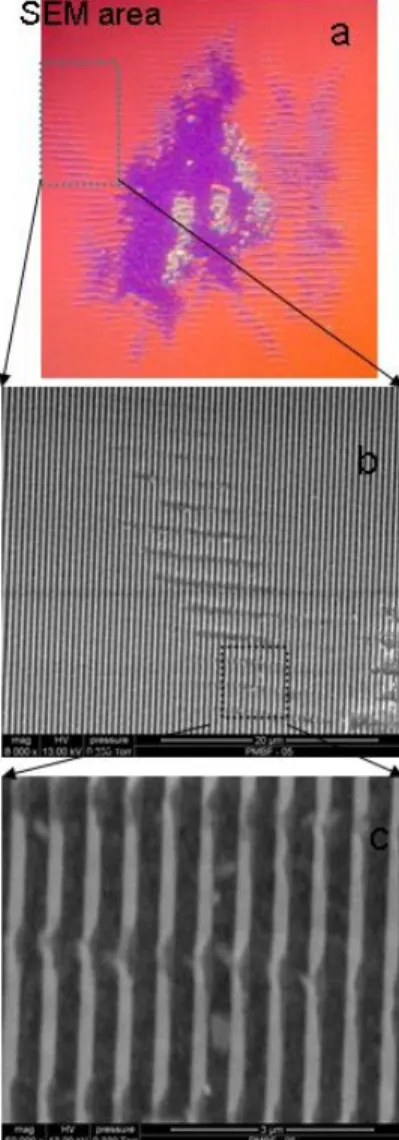
To that aim, we used the DERIC damage testing facil-ity [10] and we set the 10Hz-laser at a fluence close to the LIDT of the grating (about 3J/cm2 in normal beam). Experimentally, the grating was tested at its nominal conditions, i.e. incidence angle of 77.2 deg and TE polar-ization. Every damage test site was exposed to 100 laser pulses. Among the tested sites, we only consider small defects to observe damage with mainly initiation and some limited growth on the top layer. To select damage sites, observations must achieve a submicron resolution and they are performed with the a Nomarsky microscopy set-up associated with a scanning electron microscope (Quanta 200 from FEI, with an optimal resolution of 3 nm at 30 Kv. Images of Fig.3 are obtained at 13 Kv with low vacuum of 0,33 Torr). Results are presented in Fig. 3 at three different scales. Ripples can be observed
near the main damage site, where the fluence is close to LIDT and damage initiates (Fig.3a), and they are per-pendicular to the grating line (Fig.3b). Fig.3c unveils the important result that damage initiates at the ripples lo-cation, where the electric field is locally over enhanced. Fig.3c also remarkably reveals that damage initiates on the edge of the pillar grating, at the opposite side of the illuminating beam, where the enhancement of the elec-tric field is maximum (see Fig. 2). This microscopic ob-servation definitely proves the link between electric field enhancement and damage initiation.
Fig. 3. Scanning Electrons micrography images of the damage sites with increasing scales (a-c). (a) The ripples of period 2.5 µm are visible near the main damage site. (b) They are perpendicular to the grating lines and (c) are responsible for the initiation damage. Incoming wave is coming from left to right.
However, it is clearly visible in Fig. 3 that during the initiation, the damage structure is spatially mod-ulated perpendicularly to the grating lines with a period of about 2.5 µm. These modulations are called ripples and have been oftenly observed on fs-damaged facility on MLD gratings from various suppliers [10], [14] or on
tilayer dielectric mirrors [15]. Noteworthy, Fig.3c clearly shows that the damage initiates with the ripple struc-ture. Multiple pulse shots then make ripples grow and be more visible to become finally a large and catastrophic damage site. Ripples are attributed to the interference of surface waves propagating along the direction of the incident electric field and the illuminated beam [16]. The coupling of this surface wave to the incident propagat-ing beam is allowed by the presence of roughness at the surface of the grating (see Fig.1) . This role of roughness is also emphasized by the fact that ripples are clearly visible on MLD gratings (high roughness surfaces), less visible on MLD coatings [15] and invisible on superpol-ished fused silica substrates [7]. Consequently, the pres-ence of ripples decreases the LIDT compared to that pre-dicted by the enhancement of the electric field intensity inside the pillars, and it can be expected that the lift-ing of roughness would significantly increase the LIDT of MLD gratings. Lastly, we investigated the influence of the incident polarization by illuminating the grating in TM polarization. LIDT is in this case increased up to 4.8 J/cm2in normal beam and Fig.4b shows the absence of ripples.
(a)
(b)
Fig. 4. SEM images of damages in TE (top) and TM (bottom) polarization. The ripples are clearly observable in TE polarization, perpendicularly to the grating line, but they are not visible in TM polarization. The LIDT is close to 2.9 J/cm2in normal beam in TE polarization and 4.8 J/cm2 in normal beam in TM polarization.
We experimentally demonstrated that the local en-hancement of the electric field intensity in dielectric grat-ing pillars is responsible of the LIDT. We also empha-sized the crucial role of ripples in the initiation of the damage. This result shows that the LIDT of MLD grat-ings could be further increased by avoiding the formation of ripples at the surface of the grating. Consequently, the surface rugosity of MLD gratings is expected to play a crucial role in future developments of pulse compres-sion diffraction gratings which still limit the power of petawatt laser facilities.
Aknowledgements This work is supported by the Conseil Rgional dAquitaine, the French Ministry of Re-search and the European Union, and is performed under the auspices of the Institut Lasers et Plasmas (ILP). DE-RIC damage testing facility development was performed under the auspices of Laserlab-Europe program. We also would like to warmly thank people from PGL for grating manufacturing.
References
1. J. D. Zuegel, S. Borneis, C. Barty, B. Legarrec, C. Dan-son, N. Miyanaga, P. K. Rambo, C. Leblanc, T. J. Kessler, A. W. Schmid, L. J. Waxer, J. H. Kelly, B. Kr-uschwitz, R. Jungquist, E. Moses, J. Britten, I. Jo-vanovic, J. Dawson, and N. Blanchot, Fusion Science and Technology 49, 453–482 (2006).
2. J. P. Chambaret, F. Canova, R. Lopez-Martens,
G. Cheriaux, G. Mourou, A. Cotel, C. Le Blanc, F. Druon, P. Georges, N. Forget, F. Ple, and M. Pittman, 2007 Conference On Lasers & Electro-optics/quantum Electronics and Laser Science Conference (cleo/qels 2007), Vols 1-5 pp. 2377–2378 (2007).
3. J. Wang, Y. Jin, J. Ma, T. Sun, and X. Jing, Appl. Opt. 49, 2969–2978 (2010).
4. D. H. Martz, H. T. Nguyen, D. Patel, J. A. Brit-ten, D. Alessi, E. Krous, Y. Wang, M. A. Larotonda, J. George, B. Knollenberg, B. M. Luther, J. J. Rocca, and C. S. Menoni, Opt. Express 17, 23809–23816 (2009). 5. M. Mero, J. Liu, W. Rudolph, D. Ristau, and K. Starke,
Physical Review B 71, 115109 (2005).
6. M. D. Perry, R. D. Boyd, J. A. Britten, D. Decker, B. W. Shore, C. Shannon, and E. Shults, Opt. Lett. 20, 940– 942 (1995).
7. B. C. Stuart, M. D. Feit, S. Herman, A. M. Rubenchik, B. W. Shore, and M. D. Perry, Journal of the Optical So-ciety of America B-optical Physics 13, 459–468 (1996). 8. J. A. Britten, W. A. Molander, A. M. Komashko, and C. P. Barty, “Multilayer dielectric gratings for petawatt-class laser systems,” (SPIE, 2004), vol. 5273, pp. 1–7. 9. N. Bonod and J. Neauport, Optics Communications
260, 649–655 (2006).
10. J. Neauport, E. Lavastre, G. Raz, G. Dupuy, N. Bonod, M. Balas, G. de Villele, J. Flamand, S. Kaladgew, and F. Desserouer, Opt. Express 15, 12508–12522 (2007). 11. J. Neauport, N. Bonod, S. Hocquet, S. Palmier, and
G. Dupuy, Opt. Express 18, 23776–23783 (2010).
12. Plymouth Grating Laboratory, 5 Commerce Way,
Carver, MA 02330, United States.
13. N. Blanchot, E. Bar, G. Behar, C. Bellet, D. Bigourd, F. Boubault, C. Chappuis, H. Coic, C. Damiens-Dupont, O. Flour, O. Hartmann, L. Hilsz, E. Hugonnot, E. Lavas-tre, J. Luce, E. Mazataud, J. Neauport, S. Noailles, B. Remy, F. Sautarel, M. Sautet, and C. Rouyer, Opt. Express 18, 10088–10097 (2010).
14. T. Z. Kosc, A. A. Kozlov, and A. W. Schmid, Opt. Ex-press 14, 10921–10929 (2006).
15. S. Palmier, J. Neauport, N. Baclet, E. Lavastre, and G. Dupuy, Opt. Express 17, 20430–20439 (2009). 16. J. F. Young, J. S. Preston, H. M. van Driel, and J. E.
Sipe, Phys. Rev. B 27, 1155– (1983).