HAL Id: tel-00976632
https://tel.archives-ouvertes.fr/tel-00976632
Submitted on 10 Apr 2014HAL is a multi-disciplinary open access archive for the deposit and dissemination of sci-entific research documents, whether they are pub-lished or not. The documents may come from teaching and research institutions in France or abroad, or from public or private research centers.
L’archive ouverte pluridisciplinaire HAL, est destinée au dépôt et à la diffusion de documents scientifiques de niveau recherche, publiés ou non, émanant des établissements d’enseignement et de recherche français ou étrangers, des laboratoires publics ou privés.
Antenna designs using matching circuits for 4G
communicating devices
Aykut Cihangir
To cite this version:
Aykut Cihangir. Antenna designs using matching circuits for 4G communicating devices. Other. Université Nice Sophia Antipolis, 2014. English. �NNT : 2014NICE4010�. �tel-00976632�
1
UNIVERSITE DE NICE-SOPHIA ANTIPOLIS
ECOLE DOCTORALE STIC
SCIENCES ET TECHNOLOGIES DE L'INFORMATION ET DE LA COMMUNICATION
A
A
N
N
T
T
E
E
N
N
N
N
A
A
D
D
E
E
S
S
I
I
G
G
N
N
S
S
U
U
S
S
I
I
N
N
G
G
M
M
A
A
T
T
C
C
H
H
I
I
N
N
G
G
C
C
I
I
R
R
C
C
U
U
I
I
T
T
S
S
F
F
O
O
R
R
4
4
G
G
C
C
O
O
M
M
M
M
U
U
N
N
I
I
C
C
A
A
T
T
I
I
N
N
G
G
D
D
E
E
V
V
I
I
C
C
E
E
S
S
THESE
POUR L'OBTENTION DU GRADE DE
DOCTEUR EN SCIENCES DE L'UNIVERSITE DE NICE-SOPHIA ANTIPOLIS
PAR
AYKUT CIHANGIR
DIRECTEUR DE THESE: CYRIL LUXEY
SOUTENANCE PREVUE LE 6 MARS 2014
Jury:
M. Ala SHARAIHA, Professeur à l'
Université de Rennes (Rapporteur)
M. Laurent DUSSOPT, CEA-LETI (Rapporteur)
M. Christian PERSON, Professeur au Lab-STICC (Examinateur)
M. Frédéric Gianesello, STMicroelectronics (Examinateur)
M. Cyril LUXEY, Professeur à l’Université de Nice-Sophia-Antipolis (Directeur de thèse)
M. Fabien FERRERO, Maitre de conférences, LEAT (Co-Encadrant)
2
TABLE OF CONTENTS
CHAPTER I INTRODUCTION ... 6
1. EVOLUTIONOFCELLULARCOMMUNICATIONS ... 7
2. GENERALINFORMATIONON4GTECHNOLOGIES ... 8
3. EVOLUTIONOFMOBILEPHONEANTENNAS ... 10
4. EXAMPLESOFANTENNASINMODERNSMARTPHONES ... 13
5. THEORYOFSMALLANTENNAS ... 16
6. COUPLINGELEMENTANTENNAS ... 17
7. ANTENNASUSINGPARASITICELEMENTSFORBANDWIDTHENLARGEMENT ... 20
8. SINGLE-FEEDANDMULTI-FEEDANTENNASTRUCTURES ... 21
9. MOTIVATIONOFTHETHESIS ... 22
CHAPTER II TUNABLE ANTENNAS ... 27
1. ANTENNADESIGNSUSINGMEMSSWITCHES ... 28
1.1. ANTENNADESIGN-I ... 30
1.2. ANTENNADESIGN-II ... 40
1.3. RADIATIONEFFICIENCYDROPINANTENNAPROTOTYPES ... 45
2. ANTENNADESIGNUSINGBSTCAPACITOR ... 49
2.1. ANTENNAMODELANDSIMULATIONRESULTS ... 50
3. CONCLUSIONS ... 53
CHAPTER III THE HOLLOW COUPLING ELEMENT APPROACH ... 55
1. THE HOLLOW COUPLING ELEMENT APPROACH ... 56
1.1. COMPARISON OF THE HOLLOW CE WITH A PLAIN CE ... 56
1.2. INTEGRATION OF HIGH BAND ANTENNA WITHIN THE HOLLOW CE ... 59
1.3. PRINTED COUPLING ELEMENT ANTENNA ... 64
2. TWO-ELEMENT MIMO ANTENNA USING HOLLOW COUPLING ELEMENTS ... 70
2.1. THE LTE MIMO ANTENNA MODEL ... 71
2.2. MEASUREMENT RESULTS OF THE LTE MIMO ANTENNA ... 74
3. CONCLUSION ... 76
CHAPTER IV SINGLE FEED ANTENNAS ON LDS TECHNOLOGY ... 79
1. LOW-LTE AND UMTS ANTENNA ... 81
1.1. ANTENNA MODEL ... 81
1.2. MEASUREMENT RESULTS ... 84
2. LTE ANTENNA ... 86
2.1. ANTENNA MODEL ... 86
3
3. INVESTIGATION OF THE USER EFFECT ... 92
4. CONCLUSION ... 95
5. PERSPECTIVES ... 97
CHAPTER V EYEWEAR ANTENNAS ... 104
1. USE CASE AND GENERAL INFORMATION ON EYEWEAR DEVICES ... 105
2. FEASIBILITY STUDY FOR EYEWEAR ANTENNAS ... 106
2.1. INVESTIGATION OF BANDWIDTH POTENTIAL IN POSITION-1 ... 107
2.2. INVESTIGATION OF BANDWIDTH POTENTIAL IN POSITION-2 ... 109
2.3. INVESTIGATION OF BANDWIDTH POTENTIAL IN POSITION-3 ... 110
2.4. COMPARISON OF SAR PERFORMANCES IN THREE LOCATIONS ... 112
3. EYEWEAR ANTENNA SOLUTIONS FOR 4G COVERAGE ... 113
3.1. EYEWEAR ANTENNA-1 ... 114 3.2. EYEWEAR ANTENNA-2 ... 118 3.3. EYEWEAR ANTENNA-3 ... 121 4. CONCLUSION ... 123 5. PERSPECTIVES ... 124 CONCLUSION ... 127 FUTURE PERSPECTIVES ... 131 LIST OF FIGURES ... 136 LIST OF TABLES ... 140 PUBLICATIONS ... 141
TABLE OF ACRONYMS
CA
Carrier Aggregation
LTE
Long Term Evolution
CE
Coupling Element
MEMS
Micro Electro-Mechanical Systems
EM
Electromagnetics
MIMO
Multiple Input Multiple Output
GSM
Global System for Mobile
Telecommunications
MN
Matching Network
HB
High-Band
PCB
Printed Circuit Board
IFA
Inverted F Antenna
PIFA
Planar Inverted F Antenna
LB
Low-Band
SMD
Surface Mount Device
LDS
Laser Direct Structuring
UMTS
Universal Mobile
4
ABSTRACT
With the introduction of the fourth generation (4G) of cellular mobile communications, there has been an increase in the frequency bands that a generic mobile phone should be able to operate. This requirement poses some challenges in the design of the transceiver modules of the device as well as the RF front-end and the antenna.
From the antenna design point of view, the newly added frequency bands especially LTE bands 12-13-17 which goes down to 700MHz creates the main design challenge: covering 700-960MHz (30% bandwidth) in the low-band, considering also backward compatibility with the former technologies like GSM850/900. Since the space reserved for the antenna is electrically small in this frequency range, special design techniques are necessary to obtain the required bandwidth for a generic mobile terminal antenna.
It should also be taken into account in the design phase, that the antenna needs to be appropriate for operation in the data-rate enhancement techniques like MIMO (multiple input multiple output) and carrier aggregation in LTE-Advanced. Furthermore, considering the real use cases of the mobile terminal, the effect of the user (hand, head and both) on the antenna performance should also be investigated.
In this thesis, several antenna designs for 4G coverage in mobile terminals are proposed. Different antenna topologies are evaluated consisting of tunable/passive antennas as well as single/multi-feed structures.
The "Introduction" chapter starts with a summary about the evolution of cellular communications starting from the first analog systems evolving to the fourth generation. General information about mobile phone antennas from the past decades is then presented ending with some examples of today’s smartphone antennas. Electrically-small antennas are then presented briefly with their basic specifications and some state-of-the-art antennas for mobile terminals proposed in literature. The chapter concludes with a comparison between single-feed and multi-feed solutions with their advantages/disadvantages in LTE-Advanced technology.
Some tunable antennas, designed within the scope of the Artemos Project are presented in Chapter II. Firstly, two antenna designs using MEMS switches for band-switching between low-band (700-960MHz) and high-band (1.7-2.7GHz) are proposed, using antenna-parasitic strips for bandwidth enlargement. A circuit model is also proposed, modeling an antenna in combination with a grounded parasitic strip. A problem seen as radiation efficiency drop in these structures is also addressed with some solutions. Finally, a tunable antenna using tunable BST capacitors at the antenna feed is presented in this chapter.
A novel coupling element (CE) type antenna is proposed in Chapter III, which enables a more space-efficient design in comparison to plain CEs. First, the characteristics of the novel "hollow CE" is compared with a plain CE and two dual-feed antenna solutions are presented, using hollow CEs. As an application example, a MIMO structure using two hollow CEs is then given, using the neutralization line technique for higher isolation and lower correlation.
5 In Chapter IV, two single-feed antenna designs are proposed, manufactured using Laser Direct Structuring (LDS) technology. The first antenna can cover low-LTE/GSM/UMTS bands (700-960MHz and 1.7-2.2GHz) and the coverage of higher LTE and Wi-Fi bands (2.4-2.7GHz) is added in the second antenna. The effect of the user (hand and head) is investigated through measurements. An antenna resistant to detuning (due to the user) is then evaluated from these results as a future perspective.
A new use case of CE antennas is introduced in Chapter V, exploited to cover the 4G cellular communication bands in electronic eyewear devices, which are gaining popularity nowadays. First, a feasibility study is presented introducing the devices under design by several different companies. The bandwidth potential and SAR levels are evaluated according to different positioning of the CE in the eyewear device. Afterwards, three different antennas are proposed considering realistic casing and spectacles for the device.
Finally, a conclusion is done in Chapter VI, summarizing the general results from this thesis with some low-term and mid-term future perspectives.
6
CHAPTER
I
7
1. EVOLUTION OF CELLULAR COMMUNICATIONS
For more than thirty years, cellular communication has been under a substantial growth, according to the user demand. The first mobile communication systems were launched approximately around 1980s, giving the telephone users the freedom to make or accept calls, without the need for a fixed landline.
A cellular communication system is basically composed of three layers which are the core, the edge and the access subsystems [1]. Among these, the core is the nucleus of the network, that performs the handling of the voice calls, traffic control, user authentication and user profile (like charging the customer for the used services). The edge subsystem is an interface between the core and the access subsystems. The access subsystem (also called NodeB or Base Transceiver Station) is then responsible for establishing the air link with the mobile user equipment (UE). Different multiplexing schemes are used to serve a number of mobile users and duplexing techniques like FDD (Frequency Division Duplexing) and TDD (Time Division Duplexing) are used to establish a two-way communication (uplink and downlink) between the base station and mobile terminal. The land to be serviced is divided into some cells where these cells are served by base stations. The user can move between different cells and the handover is done automatically, transparent to the user.
The first mobile communications services (first generation or 1G) were launched in different parts of the world after 1979 [2]. These networks were based on analog systems for voice communications. The system used frequency modulation for modulating the voice signal and each user was assigned a specific frequency by Frequency Division Multiple Access (FDMA).
Approximately ten years later, the second generation of mobile communications (2G) was announced and the modulation scheme was changed from analog to digital, allowing also data transfer for services like Short Message Service (SMS). Multiple number of users were handled by using either TDMA (Time Division Multiple Access) or CDMA (Code Division Multiple Access). The most popular of the 2G standards is the GSM (Global System for Mobile Communications), which uses TDMA for multiplexing and FDD for duplex communication as uplink and downlink. GMSK (Gaussian Minimum Shift Keying) was chosen as the modulation scheme to provide better spectral efficiency. A main advantage of the GSM standard for the users was also the Subscriber Identity Module (SIM card), a card that carries the subscriber information and mobile number so that a user can change between different handset hardware by simply changing the SIM cards.
GPRS is a service launched on 2G systems, providing the user data services like MMS (Multimedia Messaging Service) and Wireless Application Protocol (WAP), making it being accepted as the 2.5G. GPRS was able to provide data rates up to 80kbit/s, which was increased later up to around 200kbit/s with the evolution to EDGE, called as the 2.75G.
With the release of the IMT-2000 standard by International Telecommunication Union, the downlink data rates of several Mbit/s started to be achieved. Systems like UMTS (W-CDMA), WiMax and CDMA2000 are examples of so-called 3G mobile communications, which introduced high-speed internet access, higher quality video and audio streaming. The most widespread radio interface is the W-CDMA using 2100MHz frequency for transmission over 5MHz bandwidth and FDD for duplexing. The downlink data rate was increased to 14Mbit/s and 28Mbit/s with the improvements called HSPA and HSPA+ (in the year 2008) respectively. A further improvement on the 3G systems towards 4G was the LTE (Long Term Evolution, 3.9G), targeting downlink data rates up to 100Mbit/s. LTE specification allows the usage of QPSK, 16QAM and 64QAM modulation types and channel bandwidth of up to 20MHz, with FDD and TDD for duplexing schemes. Additional usage of MIMO
8 (Multiple Input Multiple Output) can increase the maximum data rate from 100Mbit/s to 326Mbit/s. The access scheme used for the downlink is OFDMA (Orthogonal Frequency Division Multiple Access) for downlink and SC-FDMA (Single Carrier Frequency Division Multiple Access) for uplink.
2. GENERAL INFORMATION ON 4G TECHNOLOGIES
The successor of the 3G communication systems is the LTE-Advanced (LTE-A) which is accepted to be the fourth generation (4G) of the cellular communication systems. With this technology, the modulation schemes of QPSK, 16QAM and 64QAM are used to obtain peak data rates of up to 1Gbit/s for a low-mobility user in downlink (100Mbit/s for high mobility) and 500Mbit/s for uplink. OFDMA is used for multiple access in the downlink whereas SC-FDMA is used for uplink. The exploitation of multi-antenna systems (both for receive diversity or MIMO) is also available to reach the peak data rates. The available frequency bands for the 4G systems are shown in Figure 1, including also the 3G bands. A 4G mobile terminal should also be able to operate in the former 3G bands for backward compatibility since there is a risk of the lack a 4G base station everywhere the user may be located.
Figure 1 Frequency Allocation for 4G Systems
The LTE/4G frequency bands are presented in Table 1 and Table 2 for FDD LTE and TDD LTE respectively. It can be seen that the channel bandwidths allocated to each band is variable between 1.4MHz and 20MHz. Generally for the lower frequency bands (like bands 12 and 13) the maximum allowable channel bandwidth is up to 10MHz whereas for higher frequency bands (like band 3 or 10), bandwidths up to 20MHz is possible per channel. The multiple access scheme used in the 4G systems is OFDMA (Orthogonal Frequency Division Multiple Access), making the system more robust to fading, allowing higher data rates.
Another novelty introduced with LTE-A is the carrier aggregation, which is basically the utilization of more than one available channel for a single user. This way, the maximum achievable data rate offered to the customer can be increased. Three types of carrier aggregation are available for LTE-A as shown in Figure 2. The first type marked as (a) uses two adjacent frequency channels for a user which is called contiguous intra-band carrier aggregation. In the second type, two channels in the same band are aggregated, which are separated by other channels, making it non-contiguous intra-band carrier aggregation. Finally in the final case, two channels from two different intra-bands are used together, which is called inter-band carrier aggregation. For example for a service provider with a license for transmitting in LTE Band 2 and Band 13, it is possible to provide data to a user over these two channels (20MHz in Band 2 and 10MHz in Band 13, making a total of 30MHz maximum bandwidth) simultaneously using inter-band carrier aggregation. A maximum bandwidth allocation of 100MHz per user is possible through carrier aggregation in LTE-A.
9 Figure 2 Carrier Aggregation Methods in LTE-A
Table 1 LTE FDD Frequency Bands
LTE Band Area DL Frequency UL Frequency Bandwidth (MHz)
1 All 2110-2170MHz 1920-1980MHz 5,10,15,20 2 NAR 1930-1990MHz 1850-1910MHz 1.4,3,5,10,15,20 3 All 1805-1880MHz 1710-1785MHz 1.4,3,5,10,15,20 4 NAR 2110-2155MHz 1710-1755MHz 1.4,3,5,10,15,20 5 NAR 869-894MHz 824-849MHz 1.4,3,5,10,15,20 6 APAC 875-885MHz 830-840MHz 5,10 7 EMEA 2620-2690MHz 2500-2570MHz 5,10,15,20 8 All 925-960MHz 880-915MHz 1.4,3,5,10 9 APAC 1845-1880MHz 1750-1785MHz 5,10,15,20 10 NAR 2110-2170MHz 1710-1770MHz 5,10,15,20 11 Japan 1476-1496MHz 1428-1448MHz 5,10 12 NAR 729-746MHz 699-716MHz 1.4,3,5,10 13 NAR 746-756MHz 777-787MHz 5,10 14 NAR 758-768MHz 788-798MHz 5,10 17 NAR 734-746MHz 704-716MHz 5,10 18 Japan 860-875MHz 815-830MHz 5,10,15 19 Japan 875-890MHz 830-845MHz 5,10,15 20 EMEA 791-821MHz 832-862MHz 5,10,15,20 21 Japan 1496-1511MHz 1448-1463MHz 5,10,15 22 3510-3590MHz 3410-3490MHz 5,10,15,20 23 NAR 2180-2200MHz 2000-2020MHz 1.4,3,5,10,15,20 24 NAR 1525-1559MHz 1626.5-1660.5MHz 5,10 25 NAR 1930-1995MHz 1850-1915MHz 1.4,3,5,10,15,20 26 NAR 859-894MHz 814-849MHz 1.4,3,5,10,15 27 NAR 852-869MHz 807-824MHz 1.4,3,5,10 28 APAC 758-803MHz 703-748MHz 3,5,10,15,20 29 NAR 717-728MHz - 3,5,10 30 NAR 2350-2360MHz 2305-2315MHz 5,10 31 CALA 462.5-467.5MHz 452.5-457.5MHz 1.4,3,5
10 Table 2 LTE TDD Frequency Bands
LTE Band Area Frequency Bandwidth (MHz)
33 1900-1920MHz 5,10,15,20 34 EMEA 2010-2025MHz 5,10,15 35 NAR 1850-1910MHz 1.4,3,5,10,15,20 36 NAR 1930-1990MHz 1.4,3,5,10,15,20 37 NAR 1910-1930MHz 5,10,15,20 38 China 2570-2620MHz 5,10,15,20 39 China 1880-1920MHz 5,10,15,20 40 China 2300-2400MHz 5,10,15,20 41 All 2496-2690MHz 5,10,15,20 42 3400-3600MHz 5,10,15,20 43 3600-3800MHz 5,10,15,20 44 APAC 703-803MHz 3,5,10,15,20
3. EVOLUTION OF MOBILE PHONE ANTENNAS
The evolution of the cellular mobile communications systems have also changed the characteristics of mobile phone antennas. This evolution was sometimes driven by technical requirements like newly added frequency bands as well as user demand about aesthetical properties. Detailed analysis about the evolution of mobile terminal antennas and possible techniques are presented in [3] and [4].
Older mobile phones had an external antenna on the top of the chassis through the end of 1990s. These antennas were generally either helix type, monopole (whip) type or a combination of both for dual-band operation. The length of the whip antenna was arranged as a quarter of the operating wavelength, forming an even better configuration if the metallic chassis of the phone or the PCB was also a quarter wavelength long, therefore having a full structure like a dipole. To reduce the length of the whip antenna, a good alternative was the helical (or helix) antenna, which can be thought of the convoluted version of the whip antenna (Figure 3). To obtain a multiband structure, it was possible to use a helix antenna with a whip passing through the center axis (Figure 4), two helix antennas with different radii sharing a common axis or two helical antennas with different pitches. Despite having very good efficiency performance, the external antennas had a drawback of having high Specific Absorption Rate (SAR).
11 Figure 3 Examples of External Antenna for Mobile Phones
Figure 4 A Monopole & Helix Antenna for Mobile Phones, [3]
Through the end of 1990s, mobile phones having internal antennas started to be released on the market. Nokia released two models in 1998 and 1999 (8810 and 3210), which had internal antennas (Figure 5). One of the major internal antenna type, which was extensively used in mobile phones is the Planar Inverted F Antenna (PIFA), which can be thought of a patch antenna with a connection to the ground plane from some physical point of the antenna[5-6]. Multiband behavior was obtained easily by creating some slots in the rectangular plate to alter the current paths (Figure 6). Using some
12 parasitic elements either connected to ground plane on one end or left floating in both ends was also an alternative for multiband operation.
Figure 5 Mobile Phone Models Switching From External to Internal Antennas
Figure 6 Examples of PIFA Antennas Used in Mobile Phones [3]
Another major internal antenna type used in mobile phones was the planar monopole antennas, which do not have a direct connection to the system ground plane. This type of antennas may require a ground clearance region in the vicinity (generally on one edge of the PCB) for acceptable performance. Techniques like adding parasitic elements or adding parallel branches to the radiating element can be used for multiband operation. This type of antenna was not used in the mobile terminals until recently due to the high SAR values exceeding the limits. The opportunity to place the antenna at the bottom of the mobile phone enabled their usage, since the SAR values were now suitable due to longer distance between the antenna and head when the antenna is on the bottom of the mobile terminal.
13 Throughout the evolution of the mobile phone antennas, it was generally needed to minimize the volume/area occupied by the antenna. Techniques like etching slots or meandering were used to alter the currents on the antenna element and/or the PCB, called inductive loading. Similarly, capacitive loading was also used for this purpose, this time to manipulate the electrical near fields (like bending the antenna closer to the ground plane). Dielectric loading was also a common method by covering the vicinity of the radiating structure with a relatively high permittivity material to decrease the resonance frequency.
As new standards and new frequency bands were introduced to the mobile communication systems, antennas with wider operating frequency bandwidth in approximately the same volume were needed. Parasitic elements (either grounded or floating) which are excited capacitively by the main antenna, creating additional resonances or changing the frequencies of existing resonances could be used for bandwidth enhancement. Another common technique is also the usage of matching networks, which can either be distributed along the antenna element (for example an inductor on the grounding point of a PIFA) or introduced directly at the feed for arranging the antenna input impedance in a desired way. The matching network can be either composed of completely passive elements (like SMD capacitors and inductors), completely active elements (like a tunable varactor at the antenna feed to tune the impedance) or a combination of both.
4. EXAMPLES OF ANTENNAS IN MODERN SMARTPHONES
This section aims to presents some examples of antennas and their placement in modern smartphones. The first example is the iPhone 4GS, which uses "coupling element" type antennas, whose general properties will be detailed later in this chapter. In iPhone 4GS, the metallic portions of the phone casing (referred to as bezel) are used as radiating structures. For this purpose the bezel is split into two, longer one forming the GSM/UMTS antenna and the shorter other forming the Bluetooth/Wi-Fi/GPS antenna. However, this structure had the problem of being very sensitive to user's hand, especially when the finger is placed between the gap separating the two metallic structures.
14 In iPhone 5, the cellular antenna seen in Figure 8 was placed at the bottom of the phone and another antenna responsible for Wi-Fi operation was used at the top.
Figure 8 Antenna Placement of iPhone 5
A patent from Apple. Inc about a mobile phone antenna using again the metallic portions (bezel) of the phone casing as the radiating element can be seen in [7]. The antenna proposed in the patent is a loop antenna structure which is fed directly from the gap (shown as 18 in Figure 9), to minimize the fields across it and thus minimize any user effects due to the finger touching the gap (like the problem in iPhone 4GS). For impedance matching, a shunt inductance (formed by a metallic strip shown as 70 in the figure) and a series capacitance (shown as 100) is used at the antenna feed.
15 Another example is HTC Desire S as seen in Figure 10. This phone has three antennas realized using MID technology on plastic. The Bluetooth/Wi-Fi and GPS antennas are situated at the top of the phone whereas the IFA type pentaband antenna for GSM/UMTS is at the bottom.
Figure 10 Antenna Placement of HTC Desire S
The final example is Samsung Galaxy SII, which houses three antenna structures manufactured using MID technology, similarly as in HTC Desire S. In this phone, the GSM and Bluetooth/Wi-Fi antennas are located at the bottom and the GPS antenna is located at the top, just over the camera.
16
5. THEORY OF SMALL ANTENNAS
The popularity of internal antennas for mobile phones has gained a great popularity by the users after their introduction. This is why, the external antenna structures have quickly disappeared from the mobile terminal market. Since the frequency bands used for both GSM850/900, as well as the newly added frequency bands for LTE (like bands 12-13) go down to 700MHz, the free space wavelength rise up to 43cm for cellular communication bands. Considering the space that is available for the antenna in a mobile phone (generally lower than 20mm X 50mm X 7mm), it is evident that the antenna will be electrically small in the target frequency bands. It is also worthwhile to note that the space reserved for the antenna is subject to further decrease in smart phones having larger and larger touch screens and more and more electronic components to be placed like USB connector, camera, battery etc. The main drawback of an electrically small antenna is the low real part and high imaginary part of impedance, which makes it naturally narrowband. Electrically small antennas have been largely investigated in the literature [8-13].
A fundamental and intrinsic parameter of an electrically small antenna is its Quality Factor (Q), which is defined as the ratio of 2π times the energy stored in the near fields excited by the antenna to the energy radiated plus dissipated per cycle. The potential bandwidth of an antenna is inversely proportional to its quality factor, which results in low bandwidth potential for a high-Q antenna. The lowest obtainable radiation quality factor can be calculated from Equation-1 which is known as the Chu limit for electrically small antennas.
Q
r=
1(ka)3
+
1(ka) (Equation-1)
where k is the wavenumber (2π/λ) and a is the radius of the smallest sphere that can enclose the antenna. It is necessary to note that this value is an optimistic theoretical value considering a linearly polarized antenna radiating only in one (TE or TM) mode.
FBW =
1Q
�
(TS−1)(S−T)
S
(Equation-2)
The obtainable frequency bandwidth can be calculated from Equation-2 as also presented in [14], where S is the maximum target VSWR and T is the coupling coefficient as given in [15]. For a value of T=1, Equation 2 reduces to:
BW
cc=
1Q (S−1)
√S
(Equation-3)
This situation is called the "critically coupled" case, where the input impedance of the antenna is matched exactly to Z0 (generally 50Ω) at a single frequency point (red curve in Figure 12). An
alternative to get higher impedance bandwidth is to get optimal overcoupling, where the antenna is not matched exactly to Z0, but matched in a wider bandwidth with a higher |s11| (for example with
-7dB instead of -15dB), still under a predetermined target reflection coefficient level (blue curve in Figure 12). Some examples of using a matching network to obtain optimally overcoupled antennas are presented in [16-17].
For the calculation of the Q-factor of an antenna from its input impedance, Equation-4 was proposed in [13], which proposes a fast and reliable calculation method.
17
Q(
ω) =
ω 2R(ω)�[R
′(
ω)]
2+
�X
′(
ω) +
|X(ω)| ω�
2 (Equation-4)where ω represents the angular frequency point, R(ω) and X(ω) stands for the real and imaginary parts of the impedance at angular frequency ω, and R'(ω) and X'(ω) are the first derivates of R(ω) and X(ω) according to the frequency. This formula is valid for a single resonant antenna close to its resonance frequency but it has proven reliable performance so far.
Figure 12 Critical Coupling vs Optimal Overcoupling
6. COUPLING ELEMENT ANTENNAS
As stated also in [18-21], the ground plane of the printed circuit board (PCB) in a mobile terminal plays the major role for radiation especially in the lower-frequency bands, where 90% of the total radiation comes from the PCB at 900MHz for instance[21]. The role of the ground plane in the lower frequency bands occurs regardless of the type of the antenna used, which is evident from the dipole-type vertically-polarized radiation pattern observed at low frequencies. The ground plane is also effective on the radiation in the higher bands being responsible for up to approximately 50% of the total radiation at 1800MHz.
Considering this fact, coupling element (CE) antennas were widely proposed mostly in the literature, to cover the cellular communication frequency bands in a mobile phone. Coupling element antennas are inherently non-resonant antennas, designed with the purpose of exciting the proper currents (chassis wavemodes) on the system ground plane [20-22]. In this antenna-scheme, the currents are induced on the PCB by capacitive excitation and the excitation is stronger close to the resonance frequencies of the PCB (which depends on its dimensions). For a 100mm ground plane length, the first chassis wavemode (longitudinal mode) occurs around 1.1GHz if a 10mm distance is set between the CE and this PCB. The feeding mechanism of the CE is similar to the one of a monopole, with no inductive contact to the PCB ground plane. In this way, the antenna-structure exhibits a low quality-factor and thus high bandwidth potential (BP) is obtained. Figure 13, which is taken from [14] explains the general behavior of a CE placed on a 100mm X 40mm ground plane without any ground clearance (CE placed directly on the ground plane). The major axis wavemodes
18 (first and second) are shown in the figure, occurring at 1.17GHz and 2.61GHz respectively. These wavemode resonances affect the input impedance of the antenna by slowing down the change of the impedance around these frequency points due to the low-Q property of the relatively wide ground plane, as presented in the smith chart. This effect can be best observed in the plotted quality factor, having some minima in these frequencies, corresponding to high bandwidth potentials. The antenna shall then be matched to the desired target frequency band using an appropriate matching network at the feed.
Figure 13 Summary of the Coupling Element Antenna Behavior
Despite the high obtainable bandwidth potential, the main drawback of this approach is the need for a tunable or a complex MN (complex in terms of design or large number of SMD components) if dual-band coverage is needed which increase the losses due to internal resistances of those SMD components. Another disadvantage is the necessity to keep the region between the CE and the ground plane clear from any metal components (ground clearance) that can distort the E-field distribution in this area and thus degrade the BP. Some CE designs targeting only the GSM/DCS/PCS/UMTS bands have been already presented in [23-24]. In [23], two CEs were placed on one of the short edges of the PCB, one responsible for the coverage of GSM frequency band (824-960MHz) and the other for DCS/PCS band (1.71-1.99GHz), with their associated MNs at each feed (Figure 14). To obtain a single feed topology in the final design, special attention was paid on the MNs, to get a high impedance behavior for the low-band MN at high-band frequency and vice versa. The two MN branches were then combined together. In [24], again a two CE configuration (called ground plane boosters) was proposed and this time, the two MN branches were connected together
19 after using notch-filters at each branch (Figure 15). In [25], two CEs which are separately fed have been used for dual-band operation for covering only GSM/DCS/PCS bands. A tunable MN topology for a CE has been proposed in [26] to cover DVB-H, GSM and UMTS frequency bands. In [27-28], two designs have been proposed to additionally cover the low LTE frequency band starting from 700MHz. Antenna proposed in [27] can cover low LTE and UMTS bands (700-960MHz and 1.7-2.2GHz) using a single CE. The matching network at the feed consists of a two-branched MN for dual-band operation, having 9 SMD components. In [28], the coverage band is increased as 700-960MHz and 1.7-2.7GHz, covering whole 4G communication band. The antenna is like a dual-feed structure, where the low-band (LB) feed uses the radiating element as a CE, whereas the high-low-band (HB) feed has an offset in the excitation region, using also the resonant properties of the radiating element (Figure 16). These two feeds are combined together to obtain a single feed, after introducing a two branch MN (of 8 lumped components) where each branch behaves as an open circuit to the other.
Figure 14 Quad-Band Coupling Element Antenna Structure in [23]
20 Figure 16 Multi-Band Mobile Terminal Antenna in [28]
7. ANTENNAS USING PARASITIC ELEMENTS FOR BANDWIDTH
ENLARGEMENT
For operation in the main 4G frequency bands, wideband antenna behavior is needed covering 30% bandwidth in the low-band (700-960MHz) and 45% bandwidth in the high-band (1.7-2.7GHz). The coverage of the low-band (LB) is more challenging since the antenna is electrically small and thus the bandwidth potential is limited. For bandwidth enhancement, antennas using different kinds of parasitic elements have also been proposed in literature [29-38]. In these antennas, the main methodology is to capacitively excite a longer metal strip connected to the ground plane through a shorter driven strip. In [29-30], a monopole driven strip is used to excite a longer parasitic element connected to the ground plane on one edge. The LB coverage is mainly achieved by the capacitive excitation of the parasitic element and the HB is covered using the driven monopole and the higher order resonances of the parasitic strip. In [31-32], the parasitic element was connected to the ground plane on both edges forming a loop, again excited by a driven strip on the other side of the PCB (Figure 17). To increase the length of the loop parasitic, meandering was used making the design more complex and sensitive to manufacturing tolerances. In the antennas proposed in [33-36], casings for the PCB were also taken into consideration, whose loss tangent vary between 0.01-0.02 (Figure 18). In this way the advantage of dielectric loading was used to be able to achieve LB coverage more comfortably. Dielectric casings were also used in the antennas proposed in [37-38], with loss tangents between 0.02 and 0.06. Although they are called as PIFAs with coupled feeds, the main idea is the same as using a monopole like exciter (without ground connection), to excite capacitively a metal strip connected to ground in one end. The possible drawback of these antennas is the relatively complicated design and complicated antenna layout, which may be a problem when the manufacturing errors are concerned.
21 Figure 17 Meandered Loop Antenna in [32]
Figure 18 Small Size 11 Band Antenna in [34]
8. SINGLE-FEED AND MULTI-FEED ANTENNA STRUCTURES
The majority of the commercial mobile phones in the market use a single feed antenna design. A study about the advantages and disadvantages of using multi-feed antenna designs compared to single feed antennas was done in [39]. In the current single feed designs, an antenna which is able to cover the required standard frequency ranges (for example GSM850/900, DCS/PCS) is connected to a "Single Pole Multi Throw" antenna switch in the RF front end. According to the communication standard used at the instant, the output of the switch (considering the receive scenario) is changed to connect the signal from the antenna to the appropriate duplexer.
22 With the introduction of LTE-A, it is possible to receive cellular communication data over two different frequency bands (carrier aggregation), meaning there can be more than one receive chain in the front-end simultaneously. For the inter-band carrier aggregation, the signals picked up by a single feed antenna (for example one at 940MHz and one at 2150MHz) should be transmitted to the front end at the same time, which is not possible with a "Single Throw" switch. The switch should have a logic to have two active throws at the same time, which may results in worse linearity performance and higher insertion loss. In addition to these, special care should be given to prevent the two different front-ends (duplexers) from loading each other since they will be connected together at the switch.
Another solution different from having more than one active throws at the antenna switch, is to add a diplexer just after the antenna in the receive path, that will direct the different frequency signals to the appropriate duplexers, for inter-band carrier aggregation. However this will also result in increased insertion loss in the front-end.
Al alternative solution to overcome these complexities using single-feed antennas for inter-band carrier aggregation is to use multi-feed antennas, for example one covering the lower frequency band (700-960MHz) and other for higher frequency band (1.7-2.7GHz). In this way, the necessity of using a complex antenna switch or a diplexer is overcome for inter-band carrier aggregation. The drawback of this approach is the isolation between the antenna feeds. Isolation should be as high as possible (targeted better than 10dB as a rule of thumb), since it can otherwise cause efficiency losses due to unwanted coupling from one antenna to the other. Obtaining good isolation is also challenging, since the space reserved for the antenna is small in terms of wavelength (especially in lower frequencies) and the separate antennas have to be placed physically close to each other.
9. MOTIVATION OF THE THESIS
This study was done within the scope of the ARTEMOS project, a European Union project with a duration of 36 months. The main aim of the project is to obtain frequency agile, multimode, multi standard RF architectures for mobile communication devices, to decrease the bill of materials and cost of the systems. This target is represented in Figure 19, where the number of RF front-ends for several different communication standards in a typical system nowadays is reduced by proposing tunable front-end modules. Another aim of the project is to design and manufacture tunable components, which are BST capacitors, MEMS switches and MEMS varactors, to be delivered to the partners working on the RF front end and the antenna element.
23
Keeping this in mind, the aim of this study is to design, manufacture and test some novel antenna topologies for handheld mobile terminals. Particular effort is to be focused on either covering the target bands with very simple antenna layouts or achieving lower reflection coefficient in the target band compared to the antennas in the literature mentioned before. Another aim is to investigate the effect of the user (hand and head) on the antenna performances and propose a novel antenna topology which minimizes these effects. Both passive and active antenna topologies are to be evaluated for the coverage of 4G frequency bands, decided as:
-Low-Band (LB): 700-960MHz -High-Band (HB):1700-2700MHz.
With this target, the frequency bands of the communication standards low-LTE, GSM850/900, DCS/PCS, WLAN2400 and high-LTE will be covered. As a rule of thumb, -6dB in free space is accepted as the target reflection coefficient for the antennas. For the maximum limit of the antenna height, 5mm is taken, to be in compliance with the trends of current smart phone designs. For the same reason, maximum dimensions around 120mm X 60mm (for length and width respectively) was accepted for the PCB that will support the antenna. For the feeding scheme, both single-feed and multi-feed antennas were evaluated.
24
REFERENCES OF THIS CHAPTER
[1] CK Toh, “4G LTE Technologies: System Concepts,” Technology White Paper, Available: http://www.alicosystems.com/4G%20LTE%20Technologies%20System%20Concepts.pdf.
[2] T.S. Rappaport, S. Sun, R. Mayzus, H. Zhao, Y. Azar, K. Wang, G.N. Wong, J.K. Schulz, M. Samimi, F. Gutierrez, “Millimeter Wave Mobile Communications for 5G Cellular: It Will Work!,” Access, IEEE , vol. 1, pp.335-349, 2013
[3] C. Rowell, E.Y. Lam, “Mobile-Phone Antenna Design,” IEEE Antennas and Propagation Magazine, Vol. 54, No. 4, August 2012, pp 14-34.
[4] M. Secmen, “Multiband and Wideband Antennas for Mobile Communication Systems, Recent Developments in Mobile Communications - A Multidisciplinary Approach,” Dr Juan P. Maícas (Ed.), ISBN: 978-953-307-910-3, InTech, DOI: 10.5772/25921.
[5] P. Ciais, C. Luxey, A. Diallo, R. Staraj, G. Kossiavas, “Pentaband internal antenna for handset communication devices,” Microw. Opt. Technol. Lett., vol. 48, pp. 1509–1512.
[6] P. Ciais, R. Staraj, G. Kossiavas, C. Luxey, “Design of an internal quad-band antenna for mobile phones,” Microwave and Wireless Components Letters, IEEE , vol.14, no.4, pp.148,150, April 2004
[7] M. Pascolini et al., “Bezel Gap Antennas,” U.S. Patent 8 270 914, September 18, 2012.
[8] L.J. Chu, “Physical Limitations of Omnidirectional Antennas,” Journal of Applied Physics, 1948, pp. 1163–1175
[9] Wheeler, H.A., “Fundamental Limitations of Small Antennas,” Proceedings of the IRE , vol.35, no.12, pp.1479,1484, Dec. 1947
[10] Collin, R.E.; Rothschild, S., “Evaluation of antenna Q, ” Antennas and Propagation, IEEE Transactions on , vol.12, no.1, pp.23,27, Jan 1964
[11] Hansen, R.C., “Fundamental limitations in antennas, ” Proceedings of the IEEE , vol.69, no.2, pp.170,182, Feb. 1981
[12] McLean, J.S., “A re-examination of the fundamental limits on the radiation Q of electrically small antennas,” Antennas and Propagation, IEEE Transactions on , vol.44, no.5, pp.672, May 1996 [13] Yaghjian, A.D.; Best, S.R., “Impedance, bandwidth, and Q of antennas”, Antennas and
Propagation, IEEE Transactions on , vol.53, no.4, pp.1298,1324, April 2005
[14] J. Holopainen, “Compact UHF-band antennas for mobile terminals:focus on modelling, implementation, and user interaction,” Ph.D. dissertation, Department of Radio Science and Engineering, AALTO University, Helsinki, 2011.
[15] H.F. Pues, A.R. van de Capelle, “An impedance-matching technique for increasing the bandwidth of microstrip antennas,” IEEE Transactions on Antennas and Propagation, Vol. 37, No. 11, November 1989, pp 1345-1354.
[16] Antoniades, M.A.; Eleftheriades, G.V., “A multiband monopole antenna using a double-tuned wheeler matching network,” Antennas and Propagation (EuCAP), 2010 Proceedings of the Fourth European Conference on , vol., no., pp.1,4, 12-16 April 2010
[17] Selvanayagam, M.; Eleftheriades, G.V., “A Compact Printed Antenna With an Embedded Double-Tuned Metamaterial Matching Network,” Antennas and Propagation, IEEE Transactions on , vol.58, no.7, pp.2354,2361, July 2010
[18] P. Vainikainen, J. Ollikainen, O. Kivekäs, and I. Kelander, Patent FI114260, Modular coupling structure for a radio device and a portable radio device, Finland, Appl. 20002529, 17.11.2000, (15.09.2004), 22 p.
25 [19] P. Vainikainen, J. Ollikainen, O. Kivekas, I. Kelander, “Performance Analysis of Small Antennas
Mounted on Mobile Handsets,” Proceedings of the COST 259 Final Workshop-Mobile and Human Body Interaction, 2000, p. 8.
[20] P. Vainikainen, J. Ollikainen, O. Kivekas, I. Kelander, “Resonator-based analysis of the combination of mobile handset antenna and chassis,” IEEE Transactions on Antennas and Propagation, vol.50, no. 10, pp.1433-1444, October 2002.
[21] J. Villanen, J. Ollikainen, O. Kivekas, P. Vainikainen, “Coupling element based mobile terminal antenna structures,” IEEE Transactions on Antennas and Propagation, vol.54, no.7, pp. 2142,2153, July 2006.
[22] J. Holopainen, R. Valkonen, O. Kivekas, J. Ilvonen, P. Vainikainen, “Broadband Equivalent Circuit Model for Capacitive Coupling Element–Based Mobile Terminal Antenna,” IEEE Antennas and Wireless Propagation Letters, vol. 9, pp. 716-719, 2010.
[23] J. Villanen, C. Icheln, P. Vainikainen, “A coupling element-based quad-band antenna structure for mobile terminals,” Microwave and Optical Technology Letters, vol. 49, no. 6, June 2007, pp. 1277–1282.
[24] A. Andujar, J. Anguera, C. Puente, “Ground Plane Boosters as a Compact Antenna Technology for Wireless Handheld Devices,” IEEE Transactions on Antennas and Propagation, vol. 59, no. 5, pp. 1668-1677, May 2011.
[25] W.L. Schroeder, P. Schmitz, C. Thome, “Miniaturization of mobile phone antennas by utilization of chassis mode resonances”, German Microwave Conference, 2006.
[26] D. Manteuffel, M. Arnold, “Considerations on configurable multi-standard antennas for mobile terminals realized in LTCC technology,” 3rd European Conference on Antennas and Propagation 2009 (EuCAP 2009), pp. 2541-2545, 23-27th March 2009.
[27] R. Valkonen, J. Ilvonen, P. Vainikainen, “Naturally non-selective handset antennas with good robustness against impedance mistuning,” 6th European Conference on Antennas and Propagation 2012 (EUCAP 2012), pp.796-800, 26-30th March 2012.
[28] R. Valkonen, J. Ilvonen, C. Icheln, P. Vainikainen, “Inherently non-resonant multi-band mobile terminal antenna,” IET Electronics Letters, vol. 49, no. 1, pp. 11-13, 3rd January 2013.
[29] F.-H. Chu, K.-L. Wong, “Internal coupled-fed loop antenna integrated with notched ground plane for wireless wide area network operation in the mobile handset,” Microwave and Optical Technology Letters, vol. 54, no. 3, pp. 599–605, March 2012.
[30] C.-W. Yang, Y.-B. Jung, C.-W. Jung, “Octaband Internal Antenna for 4G Mobile Handset,” IEEE Antennas and Wireless Propagation Letters, vol.10, pp.817-819, 2011.
[31] W-S. Chen, B-Y. Lee, Y-T. Liu, “A printed coupled-fed loop antenna with two chip inductors for the 4G mobile applications,” Microwave and Optical Technology Letters, vol. 54, no. 9, pp. 2157– 2163, September 2012.
[32] C.-W. Chiu, C.-H. Chang, Y.-J. Chi, “A meandered loop antenna for LTE/WWAN operations in a smart phone,” Progress In Electromagnetics Research C, vol. 16, pp. 147-160, 2010.
[33] S-C. Chen, K-L. Wong, “Wideband monopole antenna coupled with a chip-inductor-loaded shorted strip for LTE/WWAN mobile handset,” Microwave and Optical Technology Letters, vol. 53, no. 6, pp. 1293–1298, June 2011.
[34] S-C. Chen, K-L. Wong, “Small-size 11-band LTE/WWAN/WLAN internal mobile phone antenna,” Microwave and Optical Technology Letters, vol. 52, no. 11, pp. 2603–2608, November 2010.
26 [35] F-H. Chu, K-L. Wong, “On-board small-size printed LTE/WWAN mobile handset antenna closely integrated with system ground plane,” Microwave and Optical Technology Letters, vol. 53, no. 6, pp. 1336–1343, June 2011.
[36] C-T. Lee, K-L. Wong, “Planar Monopole With a Coupling Feed and an Inductive Shorting Strip for LTE/GSM/UMTS Operation in the Mobile Phone,” IEEE Transactions on Antennas and Propagation, vol. 58, no. 7, pp. 2479-2483, July 2010.
[37] K-L. Wong, M-F. Tu, T-Y. Wu, W-Y. Li, “Small-size coupled-fed printed PIFA for internal eight-band LTE/GSM/UMTS mobile phone antenna,” Microwave and Optical Technology Letters, vol. 52, no. 9, pp. 2123–2128, September 2010.
[38] K-L. Wong, W-Y. Chen, C-Y. Wu, W-Y. Li, “Small-size internal eight-band LTE/WWAN mobile phone antenna with internal distributed LC matching circuit,” Microwave and Optical Technology Letters, vol. 52, no. 10, pp. 2244–2250, October 2010.
[39] P. Ikonen, J. Ella, E. Schmidhammer, P. Tikka, P. Ramachadran, P. Annamaa, “Multi-feed RF
front-ends and cellular antennas for next generation smartphones,” Available at:
27
CHAPTER
II
TUNABLE
ANTENNAS
28 This section presents several tunable antenna topologies, designed for operation in the 4G-LTE frequency bands (i.e 700-960MHz, 1.7-2.7GHz). The antennas are designed and manufactured using tunable components provided by the ARTEMOS partners. To obtain tunability in the matching response, MEMS switches and BST capacitors have been considered.
1. ANTENNA DESIGNS USING MEMS SWITCHES
The utilization of MEMS switches in reconfigurable antenna design has been a popular topic in recent years, especially due to their low loss in the microwave frequency bands. The reconfigured antenna properties of the these antennas have a diversity, like pattern reconfiguration (both in single and array antennas), switching between two operating frequency bands, tuning the matching level by MEMS capacitors (varactors) and changing the properties of antenna feeding networks [1]. For example in [2], MEMS switches were used to change the ground connection point of a PIFA to achieve polarization reconfigurability. In [3-4], the switches were used to obtain reconfigurability in the operating band. Figure 20 shows the proposed reconfigurable MN topology in [3], together with the manufactured prototype in the same study.
Figure 20 MN Topology and Manufactured Prototype in [3]
There are a number of COTS products available on the market, some of which are given in [5-6] and whose RF performance specifications are mentioned in Table 3.
Table 3 Specifications of Some Available MEMS Products
MEMS-1 MEMS-2
Frequency Bandwidth DC-40GHz DC-10GHz
Insertion Loss at 2GHz -0.29dB -0.25dB
Isolation at 2GHz -34dB -45dB
Maximum RF Input Power 40dBm (cold sw.) 36dBm
Input IP3 >65dBm
Switching ON Time <10 μs <100 μs
Control Voltage 90V 35V
In this study, the MEMS switches have been evaluated to achieve band-switching between the Low-Band (700-960MHz) and High-Band (1.7-2.7GHz) of 4G communication standards. Two antenna topologies are proposed, each using a parasitic strip connected to ground for the enlargement of matching bandwidth. The two topologies are different in the way the MEMS switches are exploited. In the first design, two MEMS switches are used to select between one of the two matching network
29 (MN) branches, like in [3] and [4]. The second design uses only one MEMS switch, to select between one of the driven strips.
The MEMS switches used in this study are designed and manufactured by DELFMEMS [7], who is also a partner in the Artemos project. DelfMEMS technology is different from the other RF MEMS switches on the market, i.e. classical cantilevers free membrane) or bridges (clamped-clamped membrane). Indeed, based on a state-of-the-art IP, DelfMEMS switches enable high performances with their specific mechanical structures featuring two main innovations: a movable membrane without anchors in the substrate and two forced on/off states to obtain a push-pull behavior. The membrane used for the electromechanical function is simply supported by two pillars, and two sets of electrodes placed either side of the pillars allow the actuation of the device. As illustrated in Figure 21(on left), the two forced states are obtained when the electrostatic forces are generated with the different electrodes, respectively internal/external electrodes for a ON/OFF state. Such operation ensures good contact forces in the ON state thus reducing the contact resistance, and provides high restoring forces for the OFF state to counter potential stiction or self actuation phenomena while ensuring important isolation.
In addition to good RF characteristics, this new mechanical structure demonstrates high reliability performances mainly because of its anti-stiction capabilities and the limitation of bounces thanks to a smart use of the different internal/external electrodes.
The insertion loss of the devices is measured to be between -0.2 and -0.25dB at 2GHz (Figure 21, on right). A high level of isolation is observed in OFF state, better than 45dB below 3GHz thanks to isolated RF and DC paths and because a gap larger than the thickness of the sacrificial layer is obtained between the contacts placed on the membrane and those on the transmission line
30 Table 4 Performance Summary of MEMS switches from DELFMEMS
Parameters Value
Frequency bandwidth 0.3-5 GHz Insertion loss 0.2-0.25 dB @2GHz Reflection coeff. < -15 dB @2GHz
Isolation > 50 dB @2GHz RF power +33 dBm for cold switching
+20 dBm for hot switching Input IP3 > 70 dBm
Switching time <10 μs for actuation voltage greater than 50V Control signal level 50-70 V Switching frequency up to 10 kHz Electrostatic self-actuation
(OFF state)
< 50 V peak peak Size 3,6 mm² Packaging type silicon cap
1.1. ANTENNA DESIGN-I
The proposed antenna layout can be observed in Figure 22. The antenna is directly printed on FR4 substrate, with the PCB dimensions of 120mm X 60mm X 0.8mm. There is a ground plane of length 107mm under the substrate on one side of the PCB, leaving a ground clearance of 13mm for the antenna. The antenna is basically composed of a driven strip, which capacitively excites a parasitic strip connected to the ground plane. The parasitic strip is connected to the ground plane over an inductor (12nH), which increases the electrical length of the parasitic strip. A MN, consisting of two branches is introduced at the antenna feed (Figure 23), to tune the antenna either in the LB or in the HB. According to the states of the two SPDT (Single Pole Double Throw) switches, one of the branches is connected to the antenna feed, which matches the impedance in different frequency bands. The LB MN branch consists of two inductors, whereas the HB MN is a single capacitor.
31 Figure 23 Switchable Matching Network Topology
1.1.1. Effect of the Parasitic Strip over the Bandwidth Potential
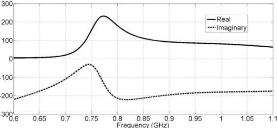
The effect of the parasitic strip has been studied in the absence of any matching network at the antenna feed. The simulated antenna input impedance with and without the parasitic strip can be observed in Figure 24, plotted between 700-960MHz. A significant increase can be noticed in the real part of the impedance, with the resonance appearing around 730MHz. Here, the term "resonance" is used to indicate a significant increase in the real part of the antenna (the loop forming in the smith chart), since under normal conditions the real part of the impedance of an electrically small antenna is low. The increase in the real part of the input impedance can be seen in Figure 25, for "with Parasitic" case.
32 Figure 25 Input Impedance (Real/Imaginary) of the Antenna With Parasitic Strip
The surface current density of the antenna presented in Figure 26 also verifies this statement. At 700MHz, the currents induced on the parasitic strip are strong, creating a current path from the driven strip to the parasitic strip and returning to the feed through ground connection. At 950MHz, the currents are significantly weaker on the parasitic element. As previously discussed, the excitation of the ground plane plays a major role in the whole radiation mechanism of the structure and therefore the radiation efficiency and also the matching coverage of the LB. When the current distribution on the ground plane is investigated, it may be concluded that the first chassis wavemode of the ground plane is excited uniformly at 950MHz.
Figure 26 Surface Currents of the Antenna and The Chassis in LB
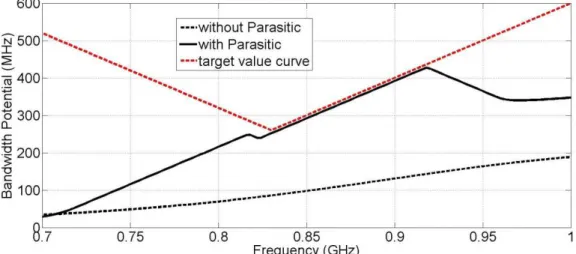
The bandwidth potential of the two cases (with/without parasitic element) has been investigated using the software Optenni Lab [8]. For this computation, the software optimizes a matching network (composed of two elements) for each frequency point and determines the frequency interval that rests under a pre-defined reflection coefficient value (-6dB chosen here). In this way, a realistic
33 bandwidth potential value is given instead of well-known, too optimistic theoretical maximum value. It can be seen in Figure 27 that introducing the parasitic strip increases the bandwidth potential considerably in the LB. The computed bandwidth potential gets closer to the target curve (in red), which states the bandwidth potential needed at each frequency point to cover 700-960MHz.The parasitic strip enables a bandwidth potential of approximately 250MHz at the center frequency (830MHz), with a two element MN.
Figure 27 Comparison of BW Potential of the antenna With/Without Parasitic Element
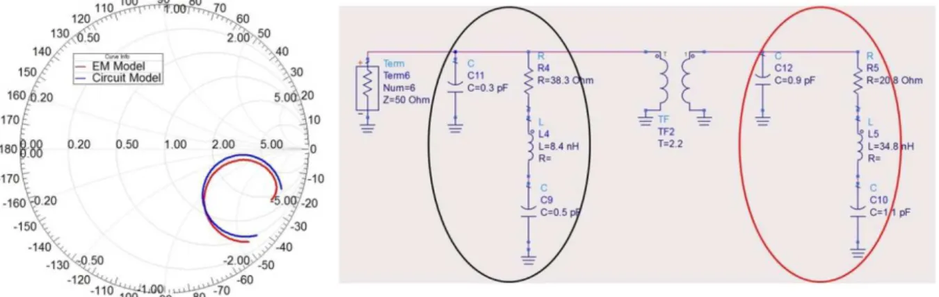
The effect of the parasitic strip for creating an additional resonance in the LB was also investigated through circuit models. Circuit models were proposed for the driven strip in the absence of parasitic strip (Figure 28 on left) and for the parasitic strip alone when it is directly fed (Figure 28 on right). The circuit models for these two configurations are modeled as a series RLC circuit with a shunt capacitor in front which represents the capacitive coupling to the ground plane. A good correspondence between the simulated EM model and the circuit models can be observed (all smith chart curves are plotted between 700-960MHz).
34 Using these two circuit models as building blocks, the circuit model in Figure 29 is obtained. The circuits for the driven strip and parasitic strip are marked with the black and red circles respectively. A transformer model is used to stand for the capacitive coupling between the strips. The creation of the resonance in the LB can be observed for the circuit model, making a good compliance with the EM simulations.
Figure 29 Circuit Model of the Combination of Driven and Parasitic Strips
The effect of the parasitic element in the HB (1.7-2.7GHz) can be observed in Figure 30. With the introduction of the parasitic element into the "driven strip only" case (red curve) two additional resonances are created around 1.85GHz and 2.4GHz. If the current distributions are observed at these two frequencies, it can be seen that the parasitic element is excited strongly in two different operating modes. Considering this fact, it can be concluded that the role of the parasitic strip is not only in the LB. It also contributes to the current distribution in the HB frequencies.
35
1.1.2. Antenna Simulations With MEMS Switches and Matching Network
The antenna whose layout has been given in Figure 22 was simulated using Ansoft HFSS [9]. In the full EM simulations, the MEMS switches and SMD components were replaced by simulation ports and measured S-parameters from the manufacturers were used at those ports with a circuit post-processing simulation done in Agilent ADS [10], to obtain more realistic results. The DC bias pads for the MEMS switches and the wirebondings (to connect the MEMS die to the traces on the PCB) were also taken into account in the full EM simulation(Figure 31).
The main criteria when optimizing the antenna was to first obtain enough bandwidth potential for the LB coverage. The main antenna parameters that were tuned for this, were the coupling gap between the driven strip and the parasitic strip, the length of the parasitic strip (that changes the frequency of the resonance) and the inductance value on the ground connection of the parasitic strip (tuning the electrical length and thus resonance frequency). Since the antenna is longer in terms of wavelength, the coverage is simpler for the HB.
The simulated input impedances of the final optimized layout, with and without MN can be seen in Figure 32, plotted for LB (700-960MHz) on left and plotted for HB (1.7-2.7GHz) on right. It is worthwhile to note that the SMD component values in the MN were tuned taking into account also the transmission lines between SMDs and also the wirebondings. To show the effect of the transmission lines between MN elements, simulation were also done by connecting the lumped elements directly in the circuit simulator (dashed curves in Figure 31) and neglecting the wirebondings. It is seen that the transmission lines might have a strong effect depending on the input impedance of the antenna before the MN.
36 Figure 32 Simulated Antenna Impedance With/Without MN (LB on left, HB on right)
The simulated reflection coefficient of the antenna can be seen in Figure 33. Without any MN, the antenna is far from being matched in the LB (red dotted curve). With proper switching of the MEMS switches to select the LB MN (black curve), the antenna can be matched in the LB with a reflection coefficient below -6dB . Likewise, by choosing the HB MN branch, the antenna has a reflection coefficient below -6dB in the HB.
Figure 33 Simulated Reflection Coefficient of the Antenna With/Without MN
1.1.3. Measurement Results for Antenna Design I
The proposed antenna has been manufactured on FR4 substrate and the integration of the MEMS switches to the PCB was done using wirebonding (Figure 34).
37 Figure 34 Pictures of the Manufactured Prototype for Antenna Design I
Due to the lack of encapsulation of the MEMS dies, problems were faced during the measurements mainly about the MEMS reliability and repeatability of the measurements. For this reason, as a backup solution, passive prototypes were manufactured where the MEMS switches are by-passed using soldered wires for ON state and left open for OFF state. The comparison of the measured reflection coefficient (for passive prototypes) and the simulation results can be seen in Figure 35 and Figure 36. A good correspondence is observed between simulations and measurements in terms of matching and input impedance behavior through both LB and HB.
38 Figure 36 Comparison of Simulated and Measured Input Impedance for Antenna Design I (LB on left,
HB on right)
The total efficiency of the passive prototype was measured in a Satimo Starlab station [11], in LB and HB (Figure 37). The measured total efficiency (including mismatch losses) can be seen in Figure 38 to be between -3.5dB and -1.5dB in the LB and between -3.5dB and -1.1dB in the HB.
39 Figure 38 Measured Total Efficiency for Antenna Design I
The comparison of the simulated and measured 3D Gain pattern for the antenna in three different frequencies can be observed in Figure 39. A good compliance is seen between the simulated and measured patterns. In the LB, a dipole type radiation is observed as expected, since the ground plane is the main radiator. The antenna becomes more directive in the HB, as the electrical length of the antenna increases. The vertical polarization (when the PCB is held vertically) is dominant in both bands, where the measured maximum gain differs by more than 10dB in the LB and around 2-4dB in the HB when compared to horizontal polarization.
Figure 39 Simulated and Measured 3D Gain Patterns for Antenna Design I
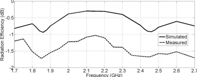
A situation about the radiation efficiency was observed, having a closer look at the HB performance of the antenna. The simulated radiation efficiency is compared with the radiation efficiency calculated from the measured total efficiency (using the measured reflection coefficient) in Figure 40. Firstly, there is a difference of approximately 0.5dB between simulated and measured radiation efficiency, whose possible cause is the accuracy of the measurement set-up given as +/-1dB
40 in the product datasheet. Besides from that, a slight drop in the radiation efficiency can be seen around 1.85GHz and 2.45GHz both in simulations and measurements. As previously stated in Figure 30, these two frequencies correspond to the strong excitation frequencies of the parasitic strip in the HB. The cause of this radiation efficiency drop was further investigated and will be explained in Section 1.3 of this chapter because it’s an important issue in many practical antenna designs for mobile phones.
Figure 40 Simulated and Measured Radiation Efficiency in HB for Antenna Design I
1.2. ANTENNA DESIGN-II
A second alternative antenna design was also proposed, using MEMS switches again for band-switching between the LB and HB. The antenna excitation methodology was changed from selecting between two MN branches to selecting between two driven strips. The proposed antenna layout can be seen in Figure 41. The antenna is directly printed on the FR4 substrate having dimensions of 115mm X 60mm X 0.8mm, with a ground clearance of 15mm for the antenna. The antenna consists of two driven strips, one for LB coverage and one for HB coverage. To increase the bandwidth potential in the LB, a parasitic element (printed under the substrate) was again used, which is capacitively excited by the LB driven strip and connected to the ground plane over an SMD inductor (18nH) on the other end. The inductor used in the ground connection helps to increase the electrical length of the parasitic strip, thus decreasing the resonance frequency created by the parasitic strip. The number of SPDT MEMS switches is reduced to one (instead of two in the former case) and the switch is used to direct the excitation current either through the LB path or the HB path as seen in Figure 41. When the LB driven strip is excited, the parasitic strip is also capacitively excited, enabling a higher bandwidth potential in the LB.
41 Figure 41 Layout of the Antenna Design-II Using MEMS Switches
1.2.1. Antenna Simulations With MEMS Switches and Matching Network
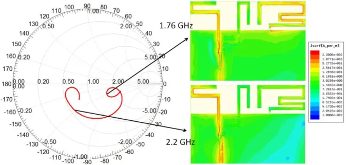
The simulated input impedance when removing the HB driven strip (considering only the LB driven strip with the parasitic element) can be observed in Figure 42 (Blue curve), on the left smith chart (plotted between 700-960MHz). A resonance is created by the parasitic strip similarly to the one created for Design I, which appears as a new loop in the smith chart. The LB response of the antenna is matched to 50Ω using a series inductor (27nH) on the LB driven strip. The red curve in the same figure presents the input impedance after the HB driven strip and the SMD inductor is introduced to the antenna. If the HB response of the antenna for "HB driven strip only" case is observed on the right smith chart, it can be seen that the parasitic strip creates a resonance in this band also at 1.76GHz.
Figure 42 Simulated Input Impedance for Antenna Design II (LB on left, HB on right)
The role of the parasitic strip in the HB can be seen with the surface currents presented in Figure 43. At 1.76GHz, strong currents are excited on the parasitic strip, which appear weaker at any other frequencies (2.2GHz presented here).
42 Figure 43 Surface Current Distribution for Antenna Design II in HB
1.2.2. Measurement Results for Antenna Design II
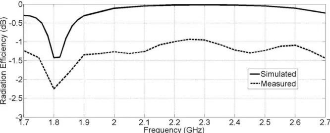
The S-parameter measurements of this prototype have been done both with real MEMS devices and with passive prototypes. In passive measurements, to represent the ON-state of the MEMS, a simple wire was soldered bypassing the MEMS and the connection was left open to represent the OFF-state. The measured reflection coefficient for the antenna in the LB and HB states can be seen in Figure 44. The target bands are covered with a reflection coefficient below -6dB in both passive measurements and real MEMS measurements, using the band-switching topology.
Figure 44 Comparison of Simulated and Measured Reflection Coefficient for Antenna Design II The simulated and measured (with passive prototypes) input impedance makes a good compliance as seen in Figure 45. Comparing the simulated impedance response with the one measured with MEMS, it can be told that the MEMS switches turned out to be more lossy in the measurements than expected, since the locus in the smith chart is closer to the center (50Ω).
43 Figure 45 Comparison of Simulated and Measured Impedance for Antenna Design II (LB on left, HB on
right)
The total efficiency of the antenna was also measured (for passive prototypes only, due to reliability issues) for LB and HB cases (Figure 47). The manufactured prototype can be observed in Figure 46.There is an efficiency higher than 3dB except around 700MHz in the LB and higher than -2.5dB in the HB.