The Design, Fabrication, and Implications of a
Solvothermal Vapor Annealing Chamber
by
Nathaniel R. Porter, Jr.
Submitted to the Department of Mechanical Engineering
in partial fulfillment of the requirements for the degree of
Bachelor of Science in Mechanical Engineering
at the
MASSACHUSETTS INSTITUTE OF TECHNOLOGY
June 2013
©
Massachusetts Institute of Technology 2013. All rights reserved.
Author ... ./ .Iepartm t ~~~~1
ARCHIVES
ASSACHUSETT , NS - UT O7ECINOLOGYJUL 3
1
2013
RARIES
of Mechanyl Engineering
May 20, 2013
j A AlC ertified by ...
David R. WallaceProfessor of Mechanical Engineering
Thesis Supervisor
Accepted by ...
Annette Hosoi Professor of Mechanical Engineering Undergraduate
Officer
The Design, Fabrication, and Implications of a Solvothermal
Vapor Annealing Chamber
by
Nathaniel R. Porter, Jr.
Submitted to the Department of Mechanical Engineering on May 20, 2013, in partial fulfillment of the
requirements for the degree of
Bachelor of Science in Mechanical Engineering
Abstract
This thesis documents the design, fabrication, use, and benefits of a prototype alu-minum solvothermal vapor annealing chamber which facilitates the self-assembly of block copolymers (BCPs) on silicon wafers which are then used to generate nanoscale patterns through the use of additive lithography. The chamber aids in the low-waste production of research and development silicon wafers possessing unparalleled surface resolution and feature density, by way of nanoscale lithography.
The concept of this chamber came out of a need by the MIT Department of Mate-rials Science and Engineering for a faster and more controlled lithographic production process. The chamber's design lends to a more simplistic, more durable, safer, and en-vironmentally cleaner process than traditional custom-made laboratory instruments. The prototype has the potential to become the standard apparatus for improving the process of solvothermal vapor annealing as a custom-built single solution.
The chamber's design is intended to enable a safer, cleaner testing environment, and provide increased control to the researcher by decoupling the temperature control of the solvent, chamber, and sample holder. As a result, the chamber has the potential to allow for a decrease in time for the production of annealed silicon wafers with more dense features than current commercial processes enable.
The chamber not only meets the required specifications of the solvothermal vapor annealing process, it also exceeds those expectations by allowing the researcher to reduce overall solvent usage. It supports an internal gage pressure of at least one atm psi and temperatures much greater than 100 degrees Celsius, both necessary conditions for the annealing process. These benefits are the direct result of five unique design characteristics.
The following unique characteristics of the solvent chamber design are: a) A tightly toleranced sliding rod;
b) A precisely machined sample-specific sized holder;
c) A modular mount for the optical film measurement device;
e) A set of bolted and press-fitted pieces of aluminum, PTFE, quartz, and copper serve to contain the highly flammable gases, toluene and heptane, normally present in this process, safeguarding the researcher.
Although the chamber has not been fully tested in an end-to-end solvothermal vapor annealing process, it demonstrates in self-testing to be a viable alternative and promising solution for Kevin Gotrik, Ph.D. Candidate in the Materials Science and Engineering.
There is potential for modifications based on user feedback and implementation. Later prototypes could explore modifying the chamber geometry, wall thickness, and sealing properties to achieve higher operating pressures and temperatures.
Thesis Supervisor: David R. Wallace Title: Professor of Mechanical Engineering
Acknowledgments
As it turns out, college is not as simple as taking classes, writing papers, and finish-ing projects. My time here at the great Massachusetts Institute of Technology has exposed me to endless opportunities as well as a great number of individuals invested in my success and happiness. This section is a tribute to all who have had a hand in growing me to the individual I am now.
For this research and design opportunity, I would like to express my deep gratitude to David R. Wallace, Professor of Mechanical Engineering, and Kevin Gotrik, Ph.D. Candidate, my thesis advisor and intended customer, for their patient guidance, en-lightening feedback, and steady encouragement throughout the development of this topic. It has been a truly wonderful experience, and will undoubtedly be a point in my life that I will warmly reflect on.
For my formal education and design experience, I formally thank the professors at MIT that I had the pleasure of meeting, working with, and learning from. Through their instruction, I have been exposed to the exciting world of Mechanical Engineering, and have had the opportunity to explore my many, varied interests. Their work with me has also awoken me to my passion for design, and instilled in me the ability to problem solve at any level.
For the exposure to manufacturing technique, I am indebted to the Pappalardo Laboratory staff and the technicians in the Laboratory for Manufacutring and Produc-tivy. Through their encouragement and patience, I have had the pleasure of gaining experience with everything from a mill, lathe, and drill, to 3D printers and circuit construction. I would like to give special thanks to Richard R. Fenner, Stephen M. Haberek, David A. Dow, and Patrick McAtamney for offering invaluable design and manufacturing suggestions for the aide in fabrication of this artifact.
For the logistical enablement of this artifact and document, I sincerely appreciate the efforts of Chevalley Duhart, Administrative Assistant to David R. Wallace, in addition to Brandy Baker and Ellen Ferrick, Mechanical Engineering Undergraduate Administrators. Ms. Duhart was a constant source of encouragement, and was able
to connect me with my thesis advisor at critical times. Both Brandy Baker and Ellen Ferrick were supportive of my endeavors and created a special deadline for this document based on my personal and educational schedule.
For the reviewing and editing of this thesis, I would like to acknoweldge David R. Wallace, Professor of Mechanical Engineering, and my mentor, Darian C. Hendricks. They were monumental resources for structuring my thoughts and developing the flow of this document.
For the supplying of materials and fabrication, I thank Ed Moriarty, Edgerton Center Instructor; McMaster-Carr Supply Company; Kevin Gotrik, Graduate Stu-dent; the MIT Department of Materials Science Engineering; and Andrew Gallant, MIT Central Machine Shop Supervisor. Mr. Moriarty provided me with material in an emergency situation when I failed to order extra material from the McMaster-Carr Supply Company. Mr. Gallant supported this project by ensuring that the welding I needed was performed in time to complete the final prototype.
For personal and emotional support, especially during difficult times in my MIT career, I thank my family, friends, the members of the MIT Gospel Choir, and my coworkers at the Robert R. Taylor Network, Inc.
This document could not have been created and developed without these individ-uals. I am incredibly grateful for their encouragment, support, and contributions.
Contents
Abstract
Acknowledgements
1 Background
2 Terms and Definitions
3 Introduction
3.1 M otivation. . . . .
3.2 Silicon and the Role in Technological Applications .
3.2.1 Optical Lithography and Masking . . . .
3.2.2 Electron Beam Lithography . . . .
3.3 Recent Advancements in Nanolithography . . . . .
3.3.1 Solvothermal Vapor Annealing Process . . . 3.4 Existing Challenges in Nanolithography . . . .
3.5 Problem Statement and Hypothesis . . . .
3.6 Proposed Solution . . . . 3.7 Research Questions and Approach . . . .
4 Solvothermal Vapor Annealing Process
4.1 T he P rocess . . . . 4.2 Process Challenges . . . . 4.3 Process Improvement: A New Chamber . . . .
3 5 15 19 21 . . . . 22 . . . . 22 . . . . 23 . . . . 23 . . . . 24 . . . . 24 . . . . 25 . . . . 25 . . . . 26 . . . . 26 29 29 30 32
5 Design and Assembly of the Solvothermal Vapor Annealing Cham-ber
5.1 Process and User Requirements with Chamber Design Specifications
5.2 Prototype 1.1: Chamber Design Schematics and Models . . . .
5.2.1 Full Assembly . . . .
5.2.2 Square Chamber . . . .
5.2.3 Sliding Rod . . . . 5.2.4 Optic Mount . . . . 5.3 Prototype 1.5 . . . .
6 Fabrication and Experimental Testing ing Chamber 6.1 Manufacturing . . . . .. . . . 6.1.1 Chamber . . . . 6.1.2 Sliding Rod . . . . 6.1.3 Optical Fixture . . . . 6.2 6.3
Assembly of Solvothermal Annealing C Equipment: Quality Testing the Cham
6.3.1 Waste Management . . . . 6.3.2 Optical Test . . . . 35 35 37 37 40
of the Solvothermal Anneal-43 . . . . 4 3 . . . . 4 4 . . . . 44 . . . . 4 6 hamber . . . . 48 ber . . . . 48 . . . . 4 8 . . . . 4 9 7 Solvothermal Vapor Annealing Process with the Prototype Cham-ber 7.1 Setup of the Solvothermal Vapor Annealing Chamber . . . . 7.2 Usage of the Solvothermal Vapor Annealing Chamber . . . . 8 Conclusions 8.1 Findings and Observations . . . . 8.2 Lessons Learned . . . . 8.3 O pen Issues . . . . 8.4 Future Steps and Recommendations . . . . 33 33 35 51 51 54 57 . . . . 58 . . . . 60 . . . . 60 . . . . 61
8.4.1 Design Chamber Enhancements . . . . 61
8.4.2 Industrialization . . . . 62
9 List of Figures 63
List of Figures
3-1 Photolithographic process steps. [4] . . . . 23
3-2 Electron Beam Lithographic process steps.
[91
. . . . 243-3 Experimental solvothermal vapor annealing system. [11] . . . . 26
4-1 The solvothermal vapor annealing process shown here, allows for the development of an extremely ordered structure. . . . . 31
5-1 Engineering drawing of the envisioned final prototype . . . . 36
5-2 3D model. Shows an acrylic box equipped with an optic fixture and enclosing an inner SVA prototype. . . . . 36
5-3 The two small holes shown here allow for solvent addition and extraction. 37 5-4 The two small holes shown here allow for the insertion of rods which can lock the sliding rod either axially or rotationally. . . . . 37
5-5 Drawing of the prototype chamber lid design. . . . . 38
5-6 Drawing of the prototype solvent chamber design. . . . . 39
5-7 Engineering schematic for the sliding rod . . . . 39
5-8 Sliding rod to allow for rapid introduction and exit of the silicon sample. 40 5-9 Drawing for the prototype design of the optic fixture. . . . . 41
5-10 Model of the expected optic fixture. . . . . 41
5-11 Prototype 1.5: final product. . . . . 42
6-1 Chamber body: a milled and bored square tube. Holes were drilled into the wall to allow the lid to be screwed on. . . . . 44
6-3 Chamber lid: hole for quartz disc and clearance holes to be mounted 6-4 6-5 6-6 6-7 6-8 6-9
to chamber body with screws. . . . . Sliding rod: intial prototype side view... Sliding rod: intial prototype top view... Sliding rod: final prototype . . . .
Sliding rod: feature to place heater in... Optical fixture: final prototype. . . . . Sample optical feedback from a substrate.[24]
. . . . 4 5 . . . . 46 . . . . 4 6 . . . . 4 6 . . . . 4 7 . . . . 4 7 . . . . 49
7-1 SVA prototype on level surface. . . . . 7-2 A thermocouple press fit into the SVA prototype. . . . . 7-3 An acceptable configuration for a resistive heating element around the SVA prottype. . . . .
7-4 The final SVA chamber setup and integration into laboratory...
7-5 Prototype SVA chamber while internal chamber becomes a saturated
vap or. . . . .
7-6 Introduce sample into chamber. . . . . 7-7 A silicon sample: post-SVA process. . . . . 9-1 Photolithographic process steps. . . . .
9-2 Electron Beam Lithographic process steps. . . . .
9-3 Experimental solvothermal vapor annealing system. . . . . 9-4 The solvothermal vapor annealing process shown here, allows for the development of an extremely ordered structure. . . . .
9-5 Engineering drawing of the envisioned final prototype .. . . . .
9-6 3D model. Shows an acrylic box equipped with an optic fixture and
enclosing an inner SVA prototype. . . . .
9-7 The two small holes shown here allow for solvent addition and extraction.
9-8 The two small holes shown here allow for the insertion of rods which can lock the sliding rod either axially or rotationally. . . . .
9-9 Drawing of the prototype chamber lid design. . . . .
52 52 53 53 54 55 55 64 64 65 66 67 67 68 68 69
9-10 Drawing of the prototype solvent chamber design. . . . . 9-11 Engineering schematic for the sliding rod .. . . . . 9-12 Sliding rod to allow for rapid introduction and exit of the silicon sample. 9-13 Drawing for the prototype design of the optic fixture. . . . .
9-14 Model of the expected optic fixture . . . ... . . . .
9-15 Prototype 1.5: final product. . . . . 9-16 Chamber body: a milled and bored square tube. Holes were drilled
into the wall to allow the lid to be screwed on. . . . .
9-17 Chamber bottom: weld to limit the possibility for leading. . . . . 9-18 Chamber lid: hole for quartz disc and clearance holes to be mounted
9-19 9-20 9-21 9-22 9-23 9-24 9-25 9-26
to chamber body with screws. . . . . Sliding rod: intial prototype side view. . . . . .
Sliding rod: intial prototype top view. . . . . .
Sliding rod: final prototype . . . .
Sliding rod: feature to place heater in. . . . . .
Optical fixture: final prototype. . . . . Sample optical feedback from a substrate.[24] . SVA prototype on level surface. . . . .
A thermocouple press fit into the SVA prototype.
9-27 An acceptable configuration for a resistive heating element around the SVA prottype. . . . . 9-28 The final SVA chamber setup and integration into laboratory... 9-29 Prototype SVA chamber while internal chamber becomes a saturated
vapor. ... ... ... ... ... ... . .... . 9-30 Introduce sample into chamber. . . . . 9-31 A silicon sample post-SVA process. . . . .
70 70 71 71 72 72 73 73 . . . . 74 . . . . 74 . . . . 74 . . . . 75 . . . . 75 . . . . 76 . . . . 77 . . . . 77 . . . . 78 78 78 79 79 80
Chapter 1
Background
The conception of this thesis orginated from a series of conversations with my Grad-uate Resident Tutor, Kevin Gotrik, a Ph.D. candidate in MIT's Materials Science and Engineering Department, around my search for a project to fulfill my thesis re-quirement for a Bachelor's of Science in the Department of Mechanical Engineering. Through these discussions, Kevin identified a need for a prototype chamber to facili-tate his research in the creation of augmented silicon wafers. Kevin Gotrik's research is part of a larger movement in the Materials Science and Engineering Department to-wards the magnetic properties of thin films and small structures, particularly for data storage and logic applications, and towards methods for creating nanoscale structures based on self-assembly and lithography.[1]
Kevin Gotrick's challenge was that he and his department did not possess a cham-ber that was: both environmentally sealed and temperature controlled. [2] He hypoth-esized that if he had a chamber to fulfill these requirements, his department would be able to proceed with research and experimental development in the regime of creating self-assembling nanoscale structures. Kevin also dictated that the process for creating these nanoscale features involved solvent vapor annealing of a substrate: silicon.[3]
As a result, I proposed the creation and development of a solvent vapor system that would solve both of his expressed concerns by decoupling temperature control between the solvent, chamber, and subtrate holder, while also minimizing exposure of the solvent vapor annealing (SVA) process to the environment. Based on prior
research, he suggested that the chamber take the form of a closed system whereby the sample could be quickly introduced into the environment, be allowed to anneal, and then be quickly removed after the solvent was thermally evaporated from the polymer film. I formed a proposal developed from these requirements, and submitted it to my thesis advisor, David R. Wallace, Professor of Mechanical Engineering.
Professor Wallace, approved the thesis proposal on the condition that my thesis would revolve around the design and fabrication of the chamber with an emphasis on the design requirements. He also encouraged me to outline a process for researching the subject matter, create a definiton for "minimal loss", and develop a way to ex-perimentally test the parameter. I proceeded to define "minimal loss" as: the only solvent vapor that escapes the chamber is the excess which surrounds the sample in the substrate holder after the completion of the solvent annealing process. The experimental verfication of minimal loss was determined through research and dis-cussion with Mr. Gotrik. After the fabrication of the chamber and introduction of solvent vapor there should be (1) no audible hissing and (2) no strong scent of the toluene solvent being utilized. With these conditions satisfied, the chamber would be chemically safe and achieve the desired process capability.
As the semester continued, I began researching the SVA process and designing the chamber in parallel. Over the course of this research and development, it became clear that I was not only developing a solvent vapor annealing chamber for a research laboratory, but developing insight to a larger market need. Through the prototyping of this chamber, I also learned how I might approach potential solutions for the continued industrial need for more rapid mass production of silicon wafers with higher surface resolution through the use of solvent vapor annealing.
The following sections: (1) introduce terms and definitions used in this paper; (2) provide information on the semiconductor industry's current manufacturing pro-cesses, in addition to Kevin Gotrik's problem and suggested solution; (3) explain the current solvothermal annealing process and its challenges; (4) describe the design and assembly of the prototype chamber to meet the researcher's requirements; (5) docu-ment the fabrication and experidocu-mental testing of the prototype; (6) instruct the user
on proper setup and operation of the device; and (7) share the analysis of results and lessons learned through this process as well as recommendations for future prototype research.
Chapter 2
Terms and Definitions
This chapter contains terms and definitions, in alphabetic order, of key concepts and ideas which are used in this thesis.
Block Copolymers: Block copolymers are made up of two unique monomer
units covalently bonded to each other. x characterizes the amount of disassociation
in the pair, and also provides insight into the probability of phase separation under the addition of solvent or temperature. These units, wanting to be disassociated, are naturally self-assembling.
Electron Beam Lithography: Electron beam lithography refers to a maskless
lithographic process which serially develops a photoresist with the use of an electron beam.
Nanolithography: Nanolithography refers to lithographic features which have a
resolution on the order of nanometers.
Photoresist: A photoresist is a light-sensitive material used in several industrial
processes, such as photolithography and photoengraving to form a patterned coating on a surface.
Optical Lithography: Optical Lithography refers to a lithographic process that
uses visible or ultraviolet light to form patterns on a photoresist.
Patterned Masks: Patterned masks are used to selectively cover the photoresist
for various printing processes. The resolution of the masks determine the resolution of photolithographic methods.
Resolution Limit: Resolution limit is the minimum feature size obtainable. In
this present document, it refers to the process capability of various types of
lithogra-phy.
Silicon Wafers: Silicon wafers are monocrystalline structures manufactured from
the melting down and pulling of natural silicon. Dopants can be added to this struc-ture in order to foster electrical conductivity.
Solvent Vapor Annealing: Solvent vapor annealing describes the process of
interaction between a solvent vapor and a polymeric substrate. This enables the monomer units to rearrange themselves into ordered structures. This process can take tens of hours, or even days. The surface resolution of this process is on the order of nanometers.
Solvothermal Vapor Annealing: Solvothermal vapor annealing is the unique
fusion of sovlent vapor annealing and thermal annealing. The polymer on the sub-strate undergoes expansion due to the exposure to the saturated vapor, which allows for the self-assembly of block copolymers. The polymer is then quenched off of the substrate through heat addition, which also serves to speed up the self-assembly as well as thermally anneal the nanolithographic structure.
Thermal Annealing: Thermal annealing describes the process of interaction
between a polymeric substrate and temperature. This addition of heat can cause the monomer units to rearrange over the course of hours. The surface resolution of this process is on the order of microns.
Chapter 3
Introduction
This chapter describes (1) the current state of nanolithographic processes, (2) the problem statement outlined by Kevin Gotrik, Ph.D. candidate in the Department of Materials Science and Engineering at the Massachusetts Institute of Technology, and
(3) the proposed solution which also meets my thesis advisor's requirements for a
senior thesis project.
Chapter 4 introduces the Solvothermal Vapor Annealing process (SVA), describes the driving factors for the process, outlines the SVA process challenges, and offers a potential solution along with the expected benefits.
Chapter 5 describes the design requirements and specifications of the prototype
SVA chamber. This section also documents the critical features for the full
function-ality of the chamber.
Chapter 6 explains the processes utilized for the fabrication and experimental testing of the prototype SVA chamber.
Chapter 7 instructs the potential user on the setup and usage of the prototype
SVA chamber. This section provides a brief overview of the chamber's enablement of
the SVA process, and the customary operating procedure.
Chapter 8 describes the observations, findings, conclusions, open issues, and rec-ommendations based on the manufacturing of the final prototype and the results of experimentation from Chapter 6.
3.1
Motivation
According to Moores Law, the number of transistors actively utilized by integrated circuits must double. Due to its continued relevance since 1958, this "law" has driven long-term goal planning for research and development around the semiconductor in-dustry. In recent years, optical lithography has been the most prominent fabrication method, allowing for resolution of features down to 50nm [4], relatively short process time, and small margin of error. Despite its strengths in commercial production, the limits of optical lithography are expected to be reached by the end of 2013. [5]
Researchers today have been working to sustain the progression of the semicon-ductor industry by re-assessing existing methods for augmenting silicon wafers. One of these processes, solvent vapor annealing (see Chapter 2), can foster a tenth of the surface resolution of the current industrial process: optical lithography. However, the process can take days or hours[6], far too slow for industry. However, through continued research and development, it has been discovered that thermal annealing, with a controlled introduction of heat, may be the answer to extension of Moores Law into the immediate future.[7]
3.2
Silicon and the Role in Technological
Applica-tions
Silicon is a gray, brittle, naturally occurring element. Perhaps one of the most im-portant uses for Silicon in the second half of the twentieth century and beyond, is its ability to conduct electricity in a very controlled manner with only a thin slice of semiconductor material, through the use of integrated circuits. The wafer serves as the the substrate for many different micro- and nanofabrication processes. Doping, etching, and photolithographic patterning are some of the common processes used to augment silicon wafers. The Silicon wafer an ideal substrate or surface for the
construction of current and future advanced semiconductor devices. In this "wafer-state", Silicon can be used for a mulitude of applicatons. However, due to the scope
Figure 3-1: Photolithographic process steps. [4]
of this project, I focused on the processes utilized by the semiconductor industry to develop nanoscale features for the development of modern technology.
3.2.1
Optical Lithography and Masking
Optical lithography is the dominant fabrication process in the production of transis-tors, computer chips, etc. It is a parallel process which exploits the properties which result from a ultra-violet beam used to expose photoresist material. This process has an excellent resolution limit of 50nm [4] and maintains a very high throughput (less than 5 seconds for the exposure phase) for industry.
Disadvantages: Roughly an hour of development time after the intial exposure
phase. Requires the use of masks fabricated by electron beam lithography in order to attain optimal feature density and precision.
3.2.2
Electron Beam Lithography
Electron Beam Lithography's prominent usage in industry is for the creation of masks for optical lithography. It has a resolution limit of just 10nm. [8]
This form of maskless, additive lithography has found wide usage in photomask-making used in photolithography, low-volume production of semiconductor compo-nents, and research and development.
e-beamn
S1 S102 (58'U) hM
Step I Clean Watei Step 2: PMMA Deposition Step 3 E-bemi Expostire
Au(I' un)
Ti (nmu)
Step 4 Developnent Step 5 Metallization Step6 Lit-off
Figure 3-2: Electron Beam Lithographic process steps.
[9]
Disadvantage: serial process which is incredibly time-instensive and dictated by
the following equation:
D * A = T * I[10] (3.1)
where D is the dose, A is the area exposed, T is the exposure time, and I is the electron beam current.
In both theory and practice, electron beam lithgoraphy is significanly more time-intensive than optical lithography. Process times for the manufacture of a single component can easily run for days.
3.3
Recent Advancements in Nanolithography
3.3.1
Solvothermal Vapor Annealing Process
The solvothermal vapor annealing (SVA) process is a fusion of two conventional pro-cesses: thermal annealing and solvent vapor annealing, and is the topic explored by Kevin Gotrik. It was chosen as the process for the development of nanolithographic applications because the unique combination of the aformentioned processes allows for increased process flexibility and decreased process times than traditional solvent annealing. Through recent experimental development, it is evident that SVA allows
for the directed, self-assembly of high x block copolymers (BCPs) with feature sizes of around 5nm.[12] Developing the precise control of the SVA process is paramount to continuing the advancement of the self-assembly of BCPs.
Advantages: maskless process, resolution limit of 5nm.
3.4
Existing Challenges in Nanolithography
None of these four lithographic processes is currently developed to a state to support the continuation of Moore's Law. As described in previous sections, optical lithog-raphy is approaching its asymptotic limit of feature resolution. Thermal annealing requires temperatures which theoretically facilitate the ordering of polymers to an feature size irreversibly degrades the substrate and solvent in reality. Solvent vapor
annealing times range in the tens of hours, and are not industrially viable. [7] The field
users of solvothermal vapor annealing lack apparati to facilitate all of the following: temperature control, a safe and clean environment, and precise measurement during the annealing process. With this thesis project, I only address solvothermal vapor annealing, due to the unique research opportunities it offers and the potential for a favorable impact on the semiconductor industry.
3.5
Problem Statement and Hypothesis
One challenge remaining with the solvothermal vapor annealing technique is that in order to reach the smallest feature sizes, a higher degree of chemical repulsion between the different blocks is required. This repulsion however can hinder and slow the motion of the BCPs and make it difficult for these polymers to self-assemble fast enough for industry to keep a profitable throughput.[13]
The issue with the experimental setup is that only temperature of the silicon wafer can be controlled. There is also no way to control the temperature of the environment, or remove the sample without waste of vapor and solvent. Also impossible to rapidly introduce the sample into a saturated vapor environment.
Figure 3-3: Experimental solvothermal vapor annealing system. [11]
3.6
Proposed Solution
To address the aforementioned challenges Kevin Gotrik and his research group are seeking to understand different methods for controlling the self-assembly of BCPs through cutting-edge solvent annealing approaches. In order to make this technique industrially viable, it is necessary for the annealing times to be further reduced and for the annealing system to have a minimal amount of waste production of potentially hazardous organic solvents.[14]
We are proposing a controlled solvent vapor annealing system that will enable further research by decoupling temperature control between the solvent, chamber, and substrate holder and by creating a closed system. Ideally, the sample will be introduced rapidly into the chamber, annealed, and then rapidly removed. We hope to accomplish such an annealing process with minimal loss of solvent outside of the solvent annealing chamber.[3]
3.7
Research Questions and Approach
In proposing the solvothermal vapor annealing chamber solution, the following high-level research questions presented themselves:
1. Is it possible to create a chamber to address both the research and
develop-mental production limits with regard to solvothermal vapor annealing? 2. Is it possible to seal this chamber from its ambient environment?
3. If so, can the design allow for rapid introduction and exit of the sample (silicon
wafer)?
4. Is it possible to decouple the temperatures for an assembly with multiple components constructed from the same material?
Subsequent chapters document my method of approach as well as my design pro-cess.
Chapter 4
Solvothermal Vapor Annealing
Process
This chapter describes the solvothermal vapor annealing (SVA) process, the current process challenges, and a hypothesized solution to address the aforementioned cir-cumstances. Kevin Gotrik was my subject matter expert in aiding me to understand the SVA process and the current documented research. He also served as my "client".
4.1
The Process
As stated in section 3.3.1, understanding and controlling the SVA process is critical for the continued improvement of the self-assembly of block copolymers (BCPs). BCPs can self-assemble into a wide variety of morphologies (cylinders, perforated lamellae, and lamellae)[15][16] because of the immiscibility between the constituent polymer units and their desire to phase separate. These structures can be exploited and utilized to improve the principle manufacturing process being discussed, additive nanolithography, down to 5nm.[17][18][19]
However, the determination of the final geometric structure, and resultant surface resolution limit, is dictated by the total length of the BCP, the Huggins interaction parameter: XAB, the volume fraction of the constituent polymer units, the solvents of choice, the thermal quenching time, and the ratio of D/Do, where Do is the initial
film thickness, and D is the maximum film thickness. [20]
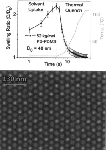
Kevin Gotrik was using the following steps to enable the SVA process with his initial experimental setup (Figure 3-3). Nitrogen was used to carry the solvents to the chamber, and for this process, the silicon wafer was sitting directly on top of a heating element (image):
(1) Add a spincoat of polydimethylsiloxane-polystyrene (PDMS-PS) polymer film
to a silicon wafer with nanoscale template posts.
(2) Insert the wafer into a completely saturated vapor environment of a heptane-toluene mixture. The mixture has a saturated vapor temperature of 25 degrees Cel-sius.
(3) Allow for the PDMS-PS polymer film to uptake solvent and swell. This takes
approximately five minutes and can cause the film to swell to three times its initial thickness.
(4) Gradually increase the wafer temperature to 115 degrees Celsius after maxi-mum film thickness has been attained. This gentle quenching of the film allows for rapid self-assembly onto the surface of the silicon sample.
The morphology resulting from the process above is shown in 9. It was developed without a mask, and is a proof of concept that ordered structures with a resolution limit of 5nm could be developed on a faster time scale than the current industry. [21] Toluene and heptane were chosen as the solvents of choice because they mix well with the BCP in use: PDMS-PS[22]. The swelling of the film allows the polymers to freely position themselves in the lowest energy state. With the introduction of heat, the structure self assembles into 9:
4.2
Process Challenges
The process posed two different categories of challenges: user and process.
Per Kevin Gotrik expressed the following challenges with the solvothermal vapor annealing process could be better facilitated with the introduction of an improved chamber design.
Solvent Thermal Uptake Quench --52 kg/mci PS-POMS' Do =48 nm I Time (s) 10
Figure 4-1: The solvothermal vapor annealing process shown here, allows for the development of an extremely ordered structure.
[11] 2-0 aD
j
100 50 I 0 - . .-Kevin's request arose from:
1. The inability to regulate and control the temperatures of the solvent vapor and
the substrate sample indepently.
2. The potential hazard and ineffiency which resulted from extended exposure of the solvent vapor to the open environment.
As the engineer to cocreate the solution, I saw an opportunity to address additional issues.
My bserving the process as the product engineer of a new solution, I noticed the
opportunity to address the following issues as well:
3. Lack of digital film measurement device.
4. Innate error due to lack of physical constraints.
Kevin Gotrik proposed that this entire process could be improved with the intro-duction of a new chamber.
4.3
Process Improvement: A New Chamber
It is believed that the introduction of an environmentally sealed, temperature con-trolled chamber would allow for real-time process feedback and process reliability.
My design philosophy was that the resulting chamber would be simplicity, durability,
and safety. Subsequent chapters document the design, assembly, fabrication, and use of the solvent vapor annealing chamber.
Chapter 5
Design and Assembly of the
Solvothermal Vapor Annealing
Chamber
This chapter describes the design and assembly of the SVA chamber to meet: (1) user specifications: the desire for an environmentally sealed and temperature controlled unit; (2) process specifications (see section 4.1): the need to support small internal pressure: 0.25 atm, temperatures up to 150 degrees C, and the rapid insertion and removal of a sample; and (3) thesis advisor's specifications: a reduction in waste, definition of "minimal loss", and testing for "minimal loss".
5.1
Process and User Requirements with
Cham-ber Design Specifications
The design requirements for the prototype chamber are as follows:
User Requirements:
-Sealed to the environment
-Enables decoupled temperature control for the solvent, chamber, and substrate holder.
Process Requirements:
-Sample must be rapidly introduced to and removed from saturated vapor envi-ronment.
-Must support temperatures up to 150 degrees C. -Must support internal pressures up to 0.25 atm.
After further research, user inquiry and collaboration, I was able to compile a list of chamber enhancements:
Chamber Enhancements:
-Process monitoring: film thickness and temperature near the substrate and poly-mer film.
-Solvent inlet and outlet: allows for easy insertion and removal of solvent.
-Extended Chamber Life: selected materials that would not be corroded by the solvent (a.k.a. non-polymers).
These requirements were translated into the following design specifications for the chamber:
Design Specifications:
1. Industrial seals, welding, or tolerance fits to keep the chamber completely
sealed.
2. Fixture should allow for attachment or embedding of stock heaters.
3. A robust seal is required to rapidly introduce and remove a sample from the
chamber.
4. Transparent crystal needs to be incoporated for the use of an optical measure-ment system.
5. No polymer can be in contact with the solvent vapor.
5.2
Prototype 1.1: Chamber Design Schematics
and Models
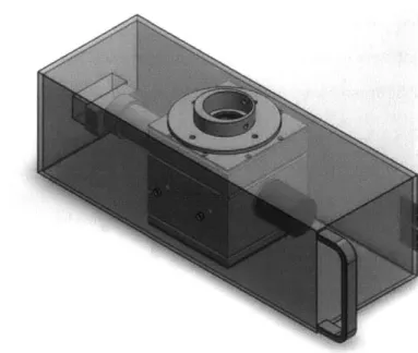
Having constructed the above design specifications, I used Solidworks 2012 and sketch-ing to iterate the product vision and design. The resultsketch-ing prototype was fabricated from the mechanical drawings and 3D models shown below. The prototype chamber was designed to be an [1] aluminum apparatus comprised of a main solvent chamber, [2] a sample holder, and [3] a fixture for an optical measurement device. Ideally, the
SVA prototype chamber was to be housed within an acrylic chamber (See Figures 5-1
and 5-2). Note: all drawings are to scale and in inches.
5.2.1
Full Assembly
This solvent vapor annealing chamber was designed to be made of solvent-safe ma-terials: steel, aluminum, or ceramic. In this case, the employment of aluminum was most appropriate, since aluminum has a high thermal conductivity. This allows the chamber to reach steady-state temperature, as well as reduce overall SVA process time. This modeled prototype addresses all of the design requirements previously mentioned. The motivation and design rationale for each piece is described in subse-quent sections and figures. More insight is provided in the manufacturing section.
5.2.2
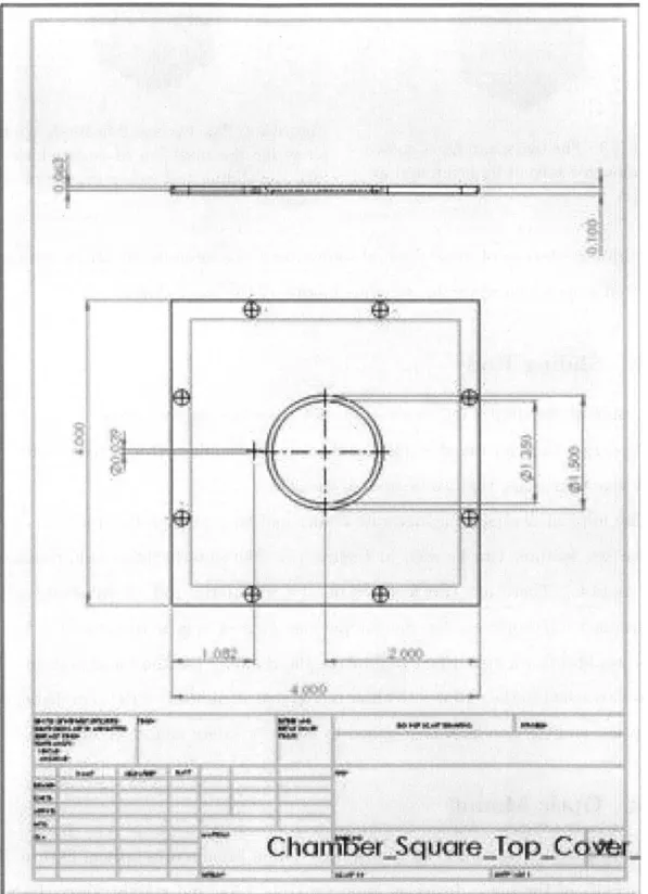
Square Chamber
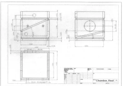
The square chamber is designed to act as the solvent holder, as well as the fixture around which the other components are sealed. As a result, it required an operative pathway for introducing and removing the sample, an external fixture to allow for the embedding of a resistive heater (Figure 5-5). I also designed holes in the side for solvent addition and removal (Figure 5-3), and holes which would allow the sliding rod to be kept from rotating during the introduction and removal of the silicon sample (Figure 5-4). To allow for the implementation of optics and a thermocouple, features were included in the chamber lid (Figure 5-6). The chamber is designed to be kept air
SuareTheds..9raWe
Figure 5-1: Engineering drawing of the envisioned final prototype.
Figure 5-2: 3D model. Shows an acrylic box equipped with an optic fixture and enclosing an inner SVA prototype.
~-0 ii ~ / 7 1W7 A"W
Figure 5-4: The two small holes shown here Figure 5-3: The two small holes shown allow for the insertion of rods which can here allow for solvent addition and ex- lock the sliding rod either axially or
rota-traction. tionally.
tight through the use of press fits and screws, and was intended to utilize industrial PTFE oil seals to allow for the dynamic motion of the inner sliding rod.
5.2.3
Sliding Rod
The design of the sliding rod was to allow for three key requirements:
-Clearance through the side holes of the solvent chamber. (tolerance of .005")
-A way to manage the two degrees of freedom
-The implementation of a substrate holder and an "optical diffractor".
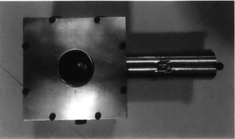
The key features can be seen in Figure 5.7. The slots facilitate non-rotational, axial motion. There are two features on the top of the rod: a substrate holder dimensioned appropriately for the sample size (1cm x 1cm x 1mm) and a feature which would diffract light when calibrating the chamber for film measurement. The magnet attached to the end was to allow repeatable alignment for the sample beneath the optics, and the handle was designed to allow for safety and ergonomic use.
5.2.4
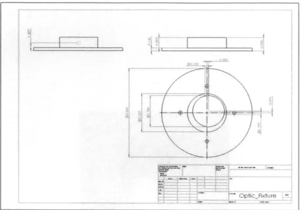
Optic Mount
The optical mount was designed to interface with a Filmmetrics optical fixture. The focal length of the optic device is approximately 2.5", and stability was the main concern for the Kevin Gotrik. As a result, this device was designed for two sets of screws: one to attach to the optics and one to attach to either the top of the chamber, or to the housing fixture. The center boss extrude was designed to allow for simple
b li
S-
J
vpa
aruf me owm..w I __Ch-aGh
bLSquarejo
pC
74
~j'Th j K
(ThI
- - CIKJrnb~v ri~oI
Figure 5-6: Drawing of the prototype solvent chamber design.
I~ 4- '*
iIIF[7
4,,.
...
~.-.,",pI
~1igRod~ iIrtao
Figure 5-8: Sliding rod to allow for rapid introduction and exit of the silicon sample.
alignment of the beam over the substrate holder: the beam used to measure film thickness is off-center from the device center (Figure 5-9).
5.3
Prototype 1.5
I went into the manufacturing lab and machined the pieces according the drawings in section 5.2. However, due to an error in manufacturing and the introduction of a time constraint, I rapidly developed and implemented a remedial solution. Below is the final result (Figure 5-11).
The next chapter discusses the fabrication process, where the complication arose, and how the chamber was physically put together.
,17j L
J,
Figure 5-9: Drawing for the prototype design of the optic fixture.
Chapter 6
Fabrication and Experimental
Testing of the Solvothermal
Annealing Chamber
This chapter documents the manufacture and assembly of the parts that comprise the final chamber.
6.1
Manufacturing
The manufacture of this chamber required machining since each component was metal.
Final List of Materials:
-1', 1.5" diameter: aluminum rod
-4" x 4" x 1' x 1/2": aluminum square hollow tube -4" x 4" x 3/8": aluminum sheet
-1" thick, 5": diameter aluminum disk
-1/2" diameter, 1':aluminum rod -4" x 3' x 1/16": aluminum sheet
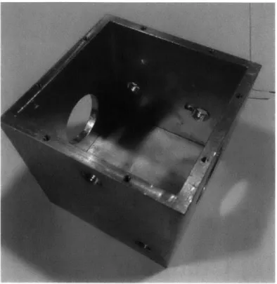
Figure 6-1: Chamber body: a milled and bored square tube. Holes were drilled into the wall to allow the lid to be screwed on.
6.1.1
Chamber
I outsourced this component to the MIT Central Machine Shop, since it required
welding (Figure 7-2). I gave them the drawing for the square chamber, and they produced the part within specification. The 3/8" plate was welded to the 1/4" square tubing. The final dimension of the square chamber was 4" x 4" x 4". They used a mill and bore to machine the holes for the sliding rod (Figure 7-1). The holes shown were expanded to allow for 1/2" - 13 plugs.
They also drilled holes into the lid and the chamber to allow the units to be screwed together. The hole in the chamber lid was developed to allow for optical measurement by the insertion of a quartz disc (Figure 7-3).
6.1.2
Sliding Rod
The sliding rod was a very critical component in this design. As one of the pieces re-sponsible for maintaining the requirement of minimum waste, the outer diameter, the
Figure 6-2: Chamber bottom: weld to limit the possibility for leading.
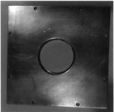
Figure 6-3: Chamber lid: hole for quartz disc and clearance holes to be mounted to chamber body with screws.
Figure 6-4: Sliding rod: intial prototype side view.
Figure 6-5: Sliding rod: intial prototype top view.
feature placement, and the seal management were all very critical. After machining prototype one, and assembling the prototype SVA chamber, I encountered an issue because I had removed an extra inch. Prototype 2 was then developed. As a way to simplify the design, and implement a locking mechanism, the lateral ends were milled to allow for screws to be inserted. These screws served as axial stops, and ensured that the substrate remained completely vertical.
Prototype 1: Prototype 2:
6.1.3
Optical Fixture
Milled the top 3/4", faced the remaining material from the bottom using a lathe.
Figure 6-7: Sliding rod: feature to place heater in.
6.2
Assembly of Solvothermal Annealing
Cham-ber
To assemble the final prototype chamber, one must put three components (chamber, substrate holder, and optic fixture) together using the following methods:
1. Insert the rod into the bored holes of the square chamber.
2. Insert screws on either end of the rod to allow for vertical allignment of the substrate holder.
3. Place the square lid on top of the chamber, and attach with 8/32 screws.
4. Place the quartz crystal into the appropriate indentation in the lid.
5. To plug the holes in the wall of the chamber, use 1/2" - 13 screws to keep the
chamber airtight when in use.
6. Manually move the modular, optical fixture to be centered over the substrate
holding feature in the rod.
Upon successful completion of the stated steps, you now have a final working SVA prototype chamber which can now be integrated into any laboratory with electricity, a table, solvent, silicon substrates and polymers.
6.3
Equipment: Quality Testing the Chamber
As a requirement for my thesis, per my advisor, I had to ensure that the waste from the chamber was minimal. I felt it necessary to ensure that my chamber met its design requirements, especially airtightness.
6.3.1
Waste Management
Because I was unable to get a full end-to-end SVA process accomplished, I tested for air tightness by filling the chamber with water. I closed the chamber lid by inserting the screws, and checked all seals. In addition, I properly oriented the chamber, and slid the rod in and out to verify the amont of waste. The only water that escaped from the chamber was that which was conatined by the substrate holder.
* j
am
SM
SM
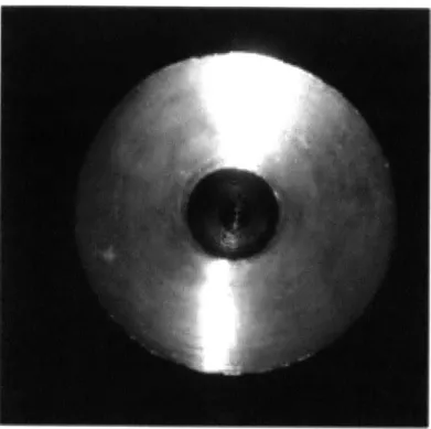
Figure 6-9: Sample optical feedback from a substrate.[24]
6.3.2
Optical Test
During the optical test, I simply setup the aluminum chamber, attached the optical measurement device to the fixture, inserted a silicon wafer, and tested to see if I was getting any sort of response. I was able to obtain optical feedback which means that the rod was locked in the proper position, and the entire assembly was centered.
Chapter
7
Solvothermal Vapor Annealing
Process with the Prototype
Chamber
This chapter outlines the setup and usage processes for the Solvothermal Vapor An-nealing Chamber.
7.1
Setup of the Solvothermal Vapor Annealing
Chamber
This process requires a certified laboratory with access to a 120V power supply in range of a non-combustible table, a multimeter, a resistive heating element, a sub-strate heater with diameter less than 2/5", a standard thermocouple, and the solvents toluene and heptane.
Step 1:
Acquire the previously assembled chamber and place on level surface.
Step 2:
Insert thermocouple into the top of the chamber to allow for precise meausrment of the polymer film and solvent temperatures.
Figure 7-1: SVA prototype on level surface.
Figure 7-3: An acceptable configuration for a resistive heating element around the
SVA prottype.
Figure 7-4: The final SVA chamber setup and integration into laboratory.
Step 3: Wrap resistive heating element around the square chamber. This heating
element will be responsible for maintaining the temperature of the solvent vapor.
Step 4: Insert the substrate heater into the sliding rod. This should be a clearance
fit. This heating element will be responsible for maintaing the tempearture of the silicon wafer.
Figure 7-5: Prototype SVA chamber while internal chamber becomes a saturated vapor.
7.2
Usage of the Solvothermal Vapor Annealing
Chamber
The usage of this chamber requires heat-insulated gloves and a liquid dropper with a diameter less than 1/2".
Step 1: Insert solvents through the solvent addition orfice. Wait for the
proto-type chamber to become a saturated vapor environment. Since this occurs at room temperature (25C), the silicon wafer should be placed in the substrate holder in the "off" position.
Step 2: Move the rod into into the "on" position, and wait approximately five minutes for the film thickness to reach a maximum. Use feedback from the real-time data acquisition device to confirm. For the next 30 seconds, the substrate heater should be gradually increased to 115 degrees Celsius.
Step 3: The polymer that was on the substrate should now be solvothermally
vapor annealed. You may now remove the sample from the SVA prototype chamber
Figure 7-6: Introduce sample into chamber.
Chapter 8
Conclusions
In Chapter 3, we hypothesized that the introduction of an environmentally sealed and temperature controlled solvent vapor annealing (SVA) chamber would allow for the continuation of research with respect to improving the process of nanolithography through the self-assembly of block copolymers (BCPs).
Through the design and fabrication of the chamber, and incorporation of user feedback, I was able to extend the contributions of the chamber to include a way to digitally monitor and provide precise control of the SVA process.
An important design principle that cannot be overlooked when creating such a chamber for R and D experiments is that the chamber itself cannot be a variable. In order to achieve that end, I specifically used tolerance fits, screws, and welds to remove ambient environmental effects. I also employed a locking mechanism on the sliding rod to ensure that the silicon sample would remain in a horizontal plane, and that the final and initial process states would be regulated.
We tested the chamber for air tightness and repeatability of optical measurement (see chapter 6). And the chamber successfully passed.
Benefits of the chamber were greater than initially hypothesized.
We also believe that this will not only satisfy Kevin Gotrik's research, but could also satisfy industry's need for a standardized apparatus to facilitate the SVA pro-cessing of block copolymers.
augment silicon wafers with nanolithography through the use of the SVA protoype chamber. However, we believe the probability of success over failure is higher than
fifty percent based on results from intial quality testing of the chamber. Aside from
adjustments or tweaks due to a full end-to-end test, there may also be user-defined needs or training and supervision required to iterate on the prototype chamber design. At the beginning of this thesis project, I formulated a hypothesis in collabora-tion with Kevin Gotrick, Materials Science researcher. We also developed four core research questions to be answered. They were:
1. Is it possible to create a chamber to address research and developmental
pro-duction limits with regard to solvothermal vapor annealing?
2. Is it possible to seal this chamber from its ambient environment?
3. If so, can the design allow for rapid introduction and exit of the sample (silicon
wafer)?
4. Is it possible to decouple the temperatures for an assembly with multiple components constructed from the same material?
In concluding this thesis, I arrived at the following findings and observations throughout this process.
8.1
Findings and Observations
After the completion of the SVA prototype chamber, I was able to resolve the majority of the initial research questions:
1. Is it possible to create a chamber to address research and developmental
pro-duction limits with regard to solvothermal vapor annealing?
I was unable to experimentally verify that the prototype chamber would further
the research of the MIT Department of Material Science and Engineering, however, we are hopeful; especially in light of the results from the initial quality testing ex-pereiment.
2. Is it possible to seal this chamber from its ambient environment?
I was able to conclude that it is, in fact, possible to seal an entirely metal chamber
from the ambient environment. This can be done throught hte use of wedling, screws, and tolerance fits.
3. If so, can the design allow for rapid introduction and exit of the sample (silicon
wafer)?
The prototype chamber was able to facilitate rapid introduction and exit of the sample holder during the experimentation with water. This was achieved by lining the metallic tolerance fit with PTFE.
4. Is it possible to decouple the temperatures for an assembly with multiple components constructed from the same material?
The decoupling of temperature for multiple components in the same assembly is feasible. This can be attained with the addition of heaters or a change in material thickness.
After going through the design process for this SVA chamber, I observed the following key principles:
-Design is an iterative and communicative process. It requires consistent commu-nication with the customer, significant amounts of research, and a desire to develop a robust solution.
- The user is not obligated to maintain his needs for an extended period of time. They can grow or diminish, and should be reflected in the iterations of the design.
- Discussion with a user is unique from observation of a user. Discussion pro-vides insight, develops relationship, and enables collaboration. Observation limits the potential for truly great design.
- Focusing on the user and his needs enabled me to see the potential for a larger commercial impact than I anticipated.
- Solidworks is unforgiving when it comes to changing critical components of the design.
8.2
Lessons Learned
The top five most important things I learned:
- User-centered design is important.
- Understanding the business value of what you are creating has tremendous im-pact.
- When designing for mass production, think about the idiot-proofing.
- I learned to put my design within the context of the larger issue.
- I validated that I really love designing and working with my hands.
- Creating stationary, circular seals to foster linear dynamics is difficult.
- Motivations changed through the development of this project. The unique in-tersection of research and personal interest
- The need for alternative suppliers or vendors
- Communication, especially listening, is important to develop a strong product.
- Learned about solvothermal vapor annealing, how polymers are selected, and how solvents are selected.
During this process, I met business people, and they opened my eyes to.. .which gave me inspiration to pursue the potential commercial applications made available through the development of this prototype.
Through this process, my passion for fabricating my thoughts was re-invigorated. engineering, business, design, I was able to document the larger picture, and place the chamber into a larger context.
not solving one person's problem, but a whole industry's personal: structuring my thoughts
8.3
Open Issues
There are only two issues that remain open from this project, and could not be answered at the writing of this paper, due to running out of time:
augmented with nanoscale lithography by an SVA process. As a result, a researcher must perform the quality test to fully assess the capabilities of the protoype.
Second, a quartz disc, intended to be embedded in the chamber lid, was not properly press fit. As a result, if this is not addressed, the chamber will not be able to sustain its seal from the ambient environment. Studies show that a small weight would be sufficient to address the lack of an airtight seal. However, It is worth noting that nearby placement of the optical fixture makes it difficult to resolve without re-machining the critical dimension.
8.4
Future Steps and Recommendations
This SVA chamber has siginificant promise for the research community in its ability to provide a standardized, environmentally sealed, and temperature controlled appa-ratus. In order to move this prototype forward to potential industrialization, there are three things that need to be done: [1] test the chamber, [2] implement the fixes to the prototype chamber (see section 8.3), [3] design and implement enhancements to the prototype chamber, and [4] research the design requirements for industrialization of the product.
8.4.1
Design Chamber Enhancements
As a stepping stone to an industrially viable solution, the following improvements should be discussed and implemented:
1. Research and implement a static seal which does not easily wear due to dynamic
motion.
2. Add an exterior handle to the rod to address the temperatures over 100 degrees Celsius.
![Figure 6-9: Sample optical feedback from a substrate.[24]](https://thumb-eu.123doks.com/thumbv2/123doknet/14722620.570817/49.918.263.648.109.495/figure-sample-optical-feedback-from-substrate.webp)