1
Development of Adhesive Bonding and Functional Testing
Systems for In-Process Inspection of Hot Embossed
Microfluidic Devices
by Caitlin J. Reyda
Sc. B. Mechanical Engineering Massachusetts Institute of Technology, 2011 Submitted to the Department of Mechanical Engineering in partial fulfillment of the requirements for the degree of
Master of Science at the
MASSACHUSETTS INSTITUTE OF TECHNOLOGY February 2014
© Massachusetts Institute of Technology 2014. All rights reserved.
Author……… Department of Mechanical Engineering
January 15, 2014
Certified by……… David E. Hardt Ralph E. and Eloise F. Cross Professor of Mechanical Engineering Thesis Supervisor
Accepted by………... David E. Hardt Ralph E. and Eloise F. Cross Professor of Mechanical Engineering Graduate Officer
3
Development of Adhesive Bonding and Functional Testing Systems for In-Process
Inspection of Hot Embossed Microfluidic Devices
by Caitlin J. Reyda
Submitted to the Department of Mechanical Engineering on January 15, 2014, in partial fulfillment of the
requirements for the degree of Master of Science
Abstract
Microfluidics has emerged as an increasingly popular field with a wide-variety of applications such as medical diagnostics, drug development, and DNA analysis. The transition of microfluidic devices from research to industry has stimulated interest in producing them at low costs and high volumes. Hot embossing has been of interest lately as a low-cost, high quality, and flexible manufacturing method that is ideal for medium-volume production. This project focuses on the continued development of a tabletop microfactory that can be used to study the control of a novel hot embossing machine. By incorporating an in-line measurement system, it would be possible to add feedback control to improve the process. This led to the design of an automated testing machine that uses an optical inspection of the microfluidic channel widths to determine embossing quality and a flow test to verify device functionality. The total cycle time of the testing machine is 85 seconds, which is well within the time of one embossing cycle (110 seconds). In order to produce complete devices for testing, an automated taping machine was also designed to seal the embossed channels. This machine took 15 seconds to complete its cycle. These two machines were integrated with the microfactory, which is currently capable of producing an embossed, sealed, and tested device every 170 seconds. The taping and width measurement processes have an error of 0.63 μm with a standard deviation of 0.82 μm. The mixing length test has an accuracy of 72.8 μm. A preliminary test demonstrated the ability to generate credible run data, and the effect of embossing temperature on width was detected to a resolution of 2 μm. The system is now able to characterize the embossing process and the effects of various embossing parameters on the final product. Closed-loop cycle-to-cycle process control can then be implemented, which will create a robust production cell that is capable of adapting to a variety of conditions.
Thesis Supervisor: David E. Hardt
5
A
CKNOWLEDGEMENTS
The work in this thesis would not have been possible without the invaluable advice, help, and support of several individuals:
I would first like to thank Prof. David Hardt for his incredible guidance and mentoring over the last few years. His enthusiasm for this project, endless quest for answers, and wealth of knowledge—whether in the laboratory or in colonial history—have truly been an inspiration.
I want to thank Maia Bageant for her company and wisdom inside the lab, during class, and out on the slopes. I want to thank Katharine Luginbuhl for working her robot magic and have the patience to deal with the occasional quirks of my machines. I want to thank Joseph Falvella for his enthusiasm while working late into the night and for keeping our work area tidy and organized.
I would also like to thank Melinda Hale and Joe Petrzelka for convincing me to join the lab in the first place and for their advice early on about research, classes, and life outside of grad school. I want to thank Monica Isava and Erin Bailie for their work in exploring early concepts of the taping machine. I want to thank Adam Libert, Scott Nill, and Larissa Nietner for the never-ending energy they bring to the lab.
I am especially grateful for the encouragement from my family and friends throughout the years and for Ben Peters who has always supported my endeavors.
Lastly, I have to thank the Singapore-MIT Alliance for generously funding this research and providing me with this amazing opportunity.
7
T
ABLE OF
C
ONTENTS
1 Introduction ... 15 1.1 Microfluidic Devices ... 15 1.2 Fabrication Methods ... 15 1.3 Process Control ... 17 1.4 Project Motivation ... 18 2 Background ... 21 2.1 Hot Embossing ... 21 2.2 Bonding ... 232.3 Measurement and Testing ... 27
3 Project History And Objectives ... 31
3.1 History of the Microfactory Project ... 31
3.2 Areas of Improvement ... 43
3.3 Current Microfactory Project Objectives ... 44
4 Design of a Taping Machine ... 45
4.1 Design Specifications ... 45
4.2 Design... 46
4.2.1 Adhesive Tape Selection... 46
4.2.2 Force Application... 49
4.2.3 Belt Drive and Take-up Reel System... 54
4.2.4 Tape Cutting... 58
4.2.5 Actuators and Sensing... 63
4.3 Completed Hardware Design ... 66
4.4 Final Taping Process ... 68
5 Measures of Quality... 69
5.1 Quality of Channel Formation... 70
5.2 Functional Test of Chips ... 71
5.3 Variation between Chips ... 72
8 6.1 Design Specifications ... 77 6.2 Design... 78 6.2.1 Optics ... 78 6.2.2 Chip Alignment ... 81 6.2.3 Fluid Flow ... 84
6.3 Completed Hardware Design ... 87
6.4 Control and Image Processing ... 89
6.5 Final Inspection Process ... 94
7 Results and Discussion ... 97
7.1 Machine Performance ... 98
7.2 Sources of Variation ... 104
7.3 Effects of Temperature on Channel Width ... 108
7.4 Mixing Location ... 109 8 Conclusion ... 115 8.1 Future Work ... 115 A Measurement Data ... 119 B Part Drawings ... 123 C System Diagrams ... 151 9 References ... 153
9
L
IST OF
F
IGURES
Figure 2-1: The steps in the hot embossing process ... 22
Figure 2-2: Cross-sectional profiles of a microfluidic channel for increasing forces... 22
Figure 2-3: A pressure sensitive film covering a 70 μm wide by 40 μm deep channel [12] ... 24
Figure 2-4: Application of a UV-curable adhesive resin using capillary action ... 25
Figure 2-5: The steps in the ultrasonic welding process ... 26
Figure 2-6: Ultrasonic welding of a 100 μm by 100 μm microfluidic channel ... 27
Figure 3-1: The final design of the micro-mixer device for the microfactory project ... 33
Figure 3-2: The first version of the microfactory ... 34
Figure 3-3: The current hot embossing machine design ... 35
Figure 3-4: The underside of the original end effector [33] ... 36
Figure 3-5: The 3-pin alignment system reduced robot positioning variation... 37
Figure 3-6: The current robot end effectors ... 38
Figure 3-7: Images of the chip and cover plate taken at different times... 39
Figure 3-8: Diagram of the high speed inspection with an angled camera ... 40
Figure 3-9: A pressure-driven functional test system for testing the micro-mixer chips ... 42
Figure 4-1: A micrograph of a chip sealed with 3M Scotch™ Magic Tape ... 47
Figure 4-2: A micrograph of a chip sealed with Tesa Tape 62551 ... 48
Figure 4-3: Scans of taped channels taken with a Zygo white light interferomete ... 49
Figure 4-4: Concept for a taping machine ... 50
Figure 4-5: Reaction forces of rollers on chips ... 51
Figure 4-6: First prototype of the taping machine ... 52
Figure 4-7: The new force application mechanism for the rollers of the taping machine ... 53
10
Figure 4-9: First prototype of the belt ... 54
Figure 4-10: The new belt with Teflon® spacers, photodiode sensor, and tensioning system ... 56
Figure 4-11: A close up of the positioning guides viewed from the front ... 56
Figure 4-12: A schematic of the tape and liner reels, taping rollers, and conveyor belt ... 57
Figure 4-13: Path of the cutting blades over the taped chips ... 58
Figure 4-14: Top view of the tape cutting assembly... 60
Figure 4-15: Front view of the tape cutting assembly ... 60
Figure 4-16: Side view of the tape cutting assembly ... 61
Figure 4-17: The completed cutting mechanism ... 62
Figure 4-18: Tape removal... 62
Figure 4-19: The final taping machine... 66
Figure 5-1: Examples of under-formed, well-formed, and over-formed devices ... 69
Figure 5-2: Top and cross-sectional views of the channels ... 71
Figure 5-4: Sample under-formed chip with bridging between channels ... 72
Figure 5-5: Locating the mixing point using pixel intensity across channels... 73
Figure 6-1: An early prototype of the functional testing system ... 78
Figure 6-2: A diagram of the new optical arrangement ... 80
Figure 6-3: A photo of the new optical arrangement ... 81
Figure 6-4: A sample image of the inspected channels ... 82
Figure 6-5: The locations of the 3 alignment pins along an embossed chip ... 82
Figure 6-6: A chip that has been clamped in the functional testing machine ... 83
Figure 6-7: Blue and yellow dye mixing in a chip to form green ... 85
Figure 6-8: Blue dye and plain water help identify the mixing location ... 85
Figure 6-9: Red dye appears darker and improves the contrast for identifying mixing ... 85
11
Figure 6-11: The final functional testing machine ... 88
Figure 6-12: The calibration curve for the 550X electronic pressure transducer ... 90
Figure 6-13: Sample recorded channel width image with measurement data overlay ... 91
Figure 6-14: Sample recorded mixing location image with measurement data overlay ... 92
Figure 6-15: Close-up images of sample channels before and after measurement ... 93
Figure 7-1: The complete microfactory system with labeled stations ... 97
Figure 7-2: Channel geometry data for a well-formed chip taken on the Zygo ... 100
Figure 7-3: Channel geometry data for an under-formed chip taken on the Zygo ... 101
Figure 7-4: A run chart of the entire system using data from the functional testing machine... 103
Figure 7-5: An x-bar chart of the data in Figure 7-4 for sample size of n=3 ... 103
Figure 7-6: An s-bar chart of the data in Figure 7-4 for sample size of n=3 ... 104
Figure 7-7: A run chart to test the variation in the functional testing machine ... 105
Figure 7-8: A histogram and normal probability plot for the data in Figure 7-6 ... 105
Figure 7-9: Run charts to test the combined variation in the taping and testing machines ... 106
Figure 7-10: Some of the variation could be caused by a build-up of dirt and plastic ... 107
Figure 7-11: The effect of embossing temperature on average channel width ... 108
Figure 7-12: Images taken of a channel on the tool using the Zygo profilometer ... 110
Figure 7-13: A 1500x SEM image of a section of a channel on the tool ... 112
13
L
IST OF
T
ABLES
Table 5-1: Estimated dye mixing lengths for a range of flow pressures ... 75
Table 6-1: Specifications for the current 10.5 MP monochrome USB microscope camera ... 79
Table 7-1: Standard deviations from measuring variability in the two machines ... 107
15
C
HAPTER
1
I
NTRODUCTION
This thesis focuses on the scale up of microfluidic device manufacturing. With the use of quick in-line measurements, the fabrication process can be controlled from cycle to cycle to produce high quality parts.
1.1 Microfluidic Devices
Microfluidics, or the manipulation of fluids in channels with dimensions of tens to hundreds of micrometers, has gained popularity in the last few decades for enabling the development of low-cost, small-footprint bioanalytical devices. These devices can already perform a wide variety of laboratory tests including high-throughput screening for drug development, polymerase chain reaction (PCR), cell sorting, medical diagnostics, and fuel cell technologies [1]. Because the amount of samples and reagents used is extremely small (10-9 to 10-18 liters), the tests can be
performed in short time periods with high resolution and sensitivity.
Despite the many current and potential applications for microfluidics, the technology is still not widely used. Many researchers have developed working designs and are ready to start producing them at a much larger scale. The transition of microfluidic technologies from research environments to industry has stimulated interest in the low-cost mass manufacturing of these devices from thermoplastic polymers. The manufacturing processes, however, are still under development as researchers try to investigate which of these processes are both feasible and economical.
1.2 Fabrication Methods
Many macro-scale polymer manufacturing processes have been adapted to form micro-scale features on microfluidic devices. Some of these are serial processes that use direct machining to remove material such as micromilling and laser ablation. These techniques are useful for
16
prototyping different microfluidic patterns, since they are extremely flexible and do not require the creation of a tool to make a new design. However, the processes themselves are extremely slow and do not scale well with larger area devices, making them poor options for mass production.
Replication techniques, on the other hand, are parallel manufacturing processes that replicate features through the use of a mold. Some examples include polydimethylsiloxane (PDMS) casting, hot embossing, injection molding, thermoforming, and ultraviolet (UV) imprinting. PDMS is not suitable as a material for mass production. It has poor dimensional stability, is not compatible with certain chemicals, and requires a two-part casting process that does not transfer well to automated production [2]. Thermoforming requires a very thin (on the order of 25 μm) film as a substrate [3]. UV imprinting uses the casting of a UV-curable resin into a mold [4]. The resin hardens after UV exposure. This process can be difficult and expensive to implement in manufacturing at a larger scale.
Injection molding is currently a common method for manufacturing microfluidic devices [3]. One of the difficulties associated with adapting this process for the micro-scale is that the injected polymer can often cool and thicken before it has a chance to fill all of the small features. This has been addressed by the use of heated molds. High quality feature replication can be achieved with carefully controlled cycle temperatures, and cycle times can be fairly short (on the order of minutes). Inserts can also be formed directly into the final parts. One of the greatest disadvantages of injection molding is the large capital cost associated with the tooling and production equipment. This is not an issue for applications that need millions of parts. However, for applications with smaller volumes (hundreds or thousands of parts) or applications with tool designs that might be revised over time, injection molding might not be the ideal option.
Hot embossing is a replication technique that addresses the low-cost, high-flexibility, medium-volume market. It is a parallel process that heats a patterned tool and a substrate to just above the glass transition temperature, Tg, of the polymer and then applies pressure, allowing the
plastic to flow into the features of the tool [4]. The two materials are then cooled and demolded. Since there is limited bulk flow of the substrate during embossing, residual stresses in the material are minimized. This makes hot embossing a suitable process for optical applications, which are sensitive to birefringence caused by residual stress. While cycle times are not quite as low as they are for injection molding, they have been improving gradually, and there might not
17
be much of a difference between their cycle times in the future [3]. Hot embossing machines are typically lower in cost than injection molding machines, and changing tooling or machine parameters is usually simpler. This is desirable for those who are looking for flexible, yet high rate manufacturing and medium volumes. An example of this would be a small company running clinical trials with a few thousand devices or researchers trying to translate their soft-polymer devices into hard-polymer designs [5].
The hot embossing process has shown great promise to be a feasible mass manufacturing technique for microfluidics, but there is still much left to be understood with regards to optimizing feature formation. This research studies parts made with hot embossing and seeks to improve the manufacturing process by implementing cycle-to-cycle process control.
1.3 Process Control
In order to improve the microfluidic manufacturing process, the system needs to be robust to disturbances. It needs to be able to adjust its parameters automatically when it detects a decrease in quality to continue producing high quality parts. To accomplish this, a measure of the device quality must be made. The results of this measurement can be used to adjust the initial forming parameters (temperature and pressure, in the case of hot embossing) until the device quality has been optimized. If a reliable measurement can be taken in a short enough period of time, the measurement can be integrated into the manufacturing process itself. If the measurement can be taken in an equal or shorter time period than the time it takes to form a part, then 100% device inspection can be achieved. This would allow real-time cycle-to-cycle process control to be implemented in the production system.
Most production systems only implement high bandwidth control of equipment parameters (such as displacement, force, temperature, and pressure) and low bandwidth control via occasional product sampling for statistical process control [6]. Systems rarely implement full in-line measurement because it is often too expensive or too complicated to achieve. However, if these measurements could be acquired, possible shifts in the mean would be detected early on, and closed-loop feedback control would allow the system to recover. Cycle-to-cycle process control would enable the system to be extremely robust and adaptive to disturbances—either in the material, the equipment, or in the environment—and product variation would be greatly reduced.
18
1.4 Project Motivation
As part of an ongoing project, a new hot embossing machine has been developed with a current cycle time of 110 seconds [7]. In order to study how cycle-to-cycle process control can be used to improve the system, a quick and reliable technique for measuring microfluidic device quality must first be developed. Current inspection techniques use high-end, metrology-grade equipment which provide extremely detailed information about feature geometry, but require a far longer measurement period than is desired.
One possibility for quickly measuring the embossing quality is with an optical inspection of the channels or other embossed features. Although transparent features can be difficult to image, it should be possible to take some sort of measurement of the feature geometries to compare between chips. Another possibility is to run a functional test of the chips. Even with a thorough visual inspection, it is difficult to know exactly how well a chip will perform as a final product. There might be slight constrictions near the inlets or variation in the surface roughness that somehow cause the device to behave better or worse. A functional test is a good method for averaging all of these variables over the distance of the entire chip instead of concentrating on discrete regions. The downside to a functional test is that the devices are typically ruined once they have been used. This is not a problem for this research because these chips are not being developed as products and 100% inspection is more desirable. In the future, functional tests could be performed much less frequently and can be coupled with a less destructive test.
In order to perform functional tests on the devices, the embossed channels first need to be sealed. This is accomplished by bonding a transparent cover plate to the embossed substrate. Significant research has been performed to study microfluidic feature formation, but sealing the devices is still a critical step in completing the manufacturing process, and an ideal bonding method has yet to be identified.
1.5 Overview of Thesis
The ultimate goal of this project is to be able to study process control on the microfluidic hot embossing process. To achieve this goal, a complete automated production cell must be developed. This thesis will focus on the development of quick, reliable bonding and testing methods that can be integrated with the current hot embossing machine to create a working factory for studying process control.
19
Chapter 2 discusses the background of hot embossing, various bonding methods, and the current microfluidic device measurement and testing methods. Chapter 3 reviews the history of the microfactory project, areas for improvement, and the current objectives that motivate this thesis. Chapter 4 covers the design of an automated taping machine that is used to seal the embossed chips before testing. Chapter 5 explains the different measurements that are being used to assess embossing quality. Chapter 6 covers the design of an automated testing machine that uses both optical inspection and functional testing to measure embossing quality. Chapter 7 reports the performance of these machines and the results of preliminary tests. Chapter 8 summarizes the accomplishments in this thesis and the next steps for the project.
21
C
HAPTER
2
B
ACKGROUND
2.1 Hot Embossing
Hot embossing creates features by plastically deforming the surface of a heated polymer substrate with a heated precision stamp. A diagram of the process can be seen in Figure 2-1. In this research, polymethylmethacrylate (PMMA)—a glassy polymer with high optical clarity, good chemical compatibility, and well characterized molding parameters—is used as the substrate. For the plastic to flow, the substrate must be heated until it is at or above its glass transition temperature, Tg (85°C to 165°C for PMMA, depending on the molecular composition)
[8]. This is done while the tool is in light contact with the substrate to reduce thermal losses and improve efficiency. The tool is then pressed into the substrate with a much higher force, allowing the viscoplastic flow of the substrate into the features of the tool. As the plastic flows in to fill the features, a front develops and gradually resembles the feature more and more with increasing pressure. This effect can be seen in Figure 2-2, which shows the cross-sectional profiles of a microfluidic channel at increasing forming forces for a constant temperature. The profile at the highest force exhibits a nearly-filled mold, whereas the profile at the lowest temperature exhibits an extremely under-formed shoulder. It should be noted that in all of these cases, the profile at the bottom of the channel remains the same.
Once the flow has been given enough time to replicate the features, the substrate and tool are cooled to below the substrate’s Tg. This allows the features to solidify as the material returns to
its glassy structure. The tool is then removed from the substrate. During cooling, the plastic exhibits shrinkage towards its center, causing the chip to adhere to the features of the tool [9]. This can cause problems if the substrate is allowed to cool for too long. Since the polymer has a higher coefficient of thermal expansion, it contracts with much larger stresses as the temperature is decreased, which can potential damage the features or the tool. On the other hand, if the substrate is demolded too quickly, adhesion forces cause the hot features to stick to sides of the
22
tool. This can also put stress on the tool and can even cause the channel edges to “smear” up slightly if the substrate has not been properly cooled. By optimize these two scenarios, the ideal demolding temperature for PMMA was calculated to be 60°C.
Figure 2-1: The steps in the hot embossing process. (1) The tool and substrate are heated to
above the Tg of the polymer. (2) A high force is applied to press the tool into the substrate, and the
plastic flows to fill the features. (3) The tool and substrate are cooled, and the part is demolded. (4) A transparent cover plate is applied to seal the channels, creating a complete device [10].
Figure 2-2: Cross-sectional profiles of a microfluidic channel for increasing forces. As the force
is increased while the forming temperature is kept constant, the plastic flows to better fill the features of the tool [8].
23
2.2 Bonding
There has been a significant amount of research dedicated towards studying the formation of microfluidic features in a variety of thermoplastics, but the devices need to be sealed before they are functional. Macro-scale thermoplastic bonding methods have been adapted to address the challenges of sealing these chips at the micro-scale. When comparing the different bonding methods, there are several properties that must be considered, depending on the applications of the particular device [11]. Bond strength is one of the most important of these, to ensure that the devices can withstand the intended flow pressures. The channels must undergo minimal deformation during the bonding process to maintain their desired geometries. The resulting exposed surface material or bond interface must be chemically compatible for the intended purpose of the device. The bonding method must be easy to implement from a manufacturing standpoint, and in many instances, the bond cannot interfere with the optical properties of the device. The bonding method must also take into consideration the means with which the device will attach to a reservoir or other connection. The cover plate might need to be more rigid than a thin film to be able to support plastic connectors.
The bonding techniques for microfluidics can be divided into two categories: indirect and direct [11]. Indirect bonding includes methods in which an intermediate layer separates two layers—at least one of which has microfluidic features. These usually involve adhesives, either as laminate films or liquid glues. Direct bonding techniques merge the surfaces of two substrates without the addition of an extra substance. These include thermal bonding, solvent bonding, and ultrasonic welding. These result in channels with homogenous sidewalls, which can be desirable in certain applications.
2.2.1 Adhesive Film Bonding
One method for sealing microfluidic channels is by covering them with a laminate film. An example of a laminate film is pressure sensitive adhesive tape. These are adhesive films with a polymer layer that can flow at room temperature, which allows a bonding surface to effectively wet, encouraging a strong bond [12]. This method is attractive because it can be fast, reliable, and inexpensive in mass production. It also does not require any heating of the substrates, which prevents feature deformation. An image of a pressure sensitive adhesive film covering part of a micro-channel is shown in Figure 2-3.
24
Figure 2-3: A pressure sensitive film covering a 70 μm wide by 40 μm deep channel [12].
Another form of laminate film uses a thermally-activated adhesive. These films can be found with an activation temperature less than the Tg of the substrate [11]. This allows the channels to
be bonded without heating up the substrate enough to deform the micro-scale features. In both of these cases, however, it is possible for the film to fill the channels, depending on the adhesive thickness and backing thickness. Also, the channels are left with a non-homogenous fourth wall. While this is not always an issue, there are cases when the reagents in a microfluidic device are sensitive to the chemical composition of the channel walls.
2.2.2 Liquid Adhesive Bonding
Glues, such as liquid adhesives (which evaporate to set) and two-part epoxies (which cure with a catalyzing agent), can be used to bond cover plates to substrates. There are not very many examples of these methods working, however, due to channels becoming easily clogged by the adhesive [11]. A more popular approach is to use high viscosity UV-curable resins instead. These synthetic resins form a bond after being exposed to UV light. The greatest challenge is also preventing the resin from clogging the channels, so many strategies have been used to control the process. One example uses capillary action to wick adhesive resin into the 5-10 μm gap of interstitial space between substrates, shown in Figure 2-4 [13]. The resin stops flowing when it reaches the larger-dimension features due to the capillary pressure drop. As with laminate film bonding, this method also results in channel walls that are no longer homogenous.
25
Figure 2-4: Application of a UV-curable adhesive resin using capillary action to prevent clogged
channels [13].
2.2.3 Thermal Bonding
With thermal bonding, a substrate and a cover plate are heated to just above the Tg of one or both
of the materials. Pressure is applied to improve the contact force between the materials. This causes polymer chains to diffuse across the surface, leading to a strong and homogenous, yet optically clear bond [11]. Because of this, thermal bonding is often viewed as a very attractive microfluidic sealing method, and there are many examples of this technique being used [14] [15] [16] [17] [18]. However, heating thermoplastics to their Tg frequently results in the collapse of
formed features. The biggest challenge, therefore, is controlling the temperature, pressure, and bonding time to prevent bulk deformation of the substrate while still achieving a strong surface bond.
2.2.4 Solvent Bonding
A material will act as a good solvent for another material when their Hildebrandt parameters, δ, are nearly equal to one another [11] 1. When a solvent is applied to a thermoplastic, the surface softens and polymer chains can diffuse across the layer and become entangled with those on the
1 The Hildebrandt solubility parameter, δ, is an estimate of the degree of interaction between materials. Materials
26
other side. This leads to exceptionally strong bonds between the two materials. However, if the δ of two materials are too similar (ie. PMMA and acetone) then extended exposure can lead to the deformation of features at the micro-scale. This can be solved by shortening the exposure time or by using slightly less similar materials.
As with liquid adhesive bonding, there are challenges with preventing the solvent from flowing into features on a chip. In one study, water was frozen in the channels to preserve their dimensional stability while a layer of solvent was applied [19]. This technique can be attractive for applications that require much higher bond strengths than can be achieved with adhesive or thermal bonding.
2.2.5 Ultrasonic Welding
Another method of mating the surfaces of an embossed thermoplastic chip and a thermoplastic cover plate is to use ultrasonic energy, which locally heats and softens the interface. Ultrasonic welding is a well-established joining process for thermoplastics at the macroscopic scale [20]. Its advantages are a quick cycle time (in the range of seconds), homogenous sidewalls, and location-specific bonding. It does not result in the same feature deformation that is typically seen with thermal bonding. This method uses 20-40 kHz ultrasonic sound waves to cause the localized melting of “energy directors”, shown in Figure 2-5, which are temporary structures to control the location of the joint.
Figure 2-5: The steps in the ultrasonic welding process. (1) The chip and cover plate are placed on a
stationary anvil. (2) A vibrating sonotrode, or “weld horn”, contacts the parts. (3)The energy directors melt and seal the chip [20].
The geometry and placement of the energy directors need to be optimized for the process, and the forming method needs to account for these additional features, but preliminary tests have
27
shown that this method is feasible [21]. Channels with cross-sectional dimensions of 100 μm wide by 100 μm deep were successfully bonded with a leak-free seal and minimal channel deformation, as seen in Figure 2-6.
Figure 2-6: Ultrasonic welding of a 100 μm by 100 μm microfluidic channel. Left: Channel before
bonding. The energy directors can be seen on either side of the channel. Right: Enclosed channel after bonding [21].
2.3 Measurement and Testing
The microfluidics manufacturing step with the least amount of documented research is the inspection or functional testing of devices for process control purposes. While there are currently businesses that provide large-volume production services for smaller microfluidics companies, there is very little information about the processes they use, particularly for inspecting their products. The businesses that do indicate some form of production control will only reveal enough to say that “each and every product is tested to ensure the quality”2. It is unclear what kind of test is performed—whether it is a simple feature inspection or a more thorough functional test—and it is unlikely that the results are being used to control the fabrication process with more than standard statistical process control.
For background on the use of in-line measurements for the control of fabrication processes, the semiconductor industry can be turned to as an example. As the fastest evolving major industry, the semiconductor industry has been at the leading edge for advanced process control technologies [22]. Historically, process parameters were left alone until a mean shift in the final output data triggered an alarm. The parameters would then be adjusted manually to correct for the change. However, this could result in many defective parts. Like microfluidic devices, semiconductor wafers require many processing steps to create functional devices. If a manufacturing defect occurs during an earlier step, there is a high probability that the resulting
28
product will also be defective. This can end up being very costly. The form of process tuning that is currently being pursued by the industry instead is cycle-to-cycle control, which takes in-line measurements throughout the manufacturing process and can immediately identify changes. It can then automatically correct for these changes based on a process model. There are still some issues that hinder the adoption of this type of control. For example, there is a lack of commercial solutions and in-line metrology sensors available to implement this control.
While it is very difficult to find research on automated high-throughput microfluidic inspection systems, there are numerous examples of inspections that have been performed in smaller batches. These are often used to characterize the performance of a new device or to verify the resolution of a new manufacturing process. Optical inspection is one of the most widely performed test methods. It can take just seconds to capture images, and it is also possible to observe the chips while they are being functionally tested. The entire test set-up can be placed on a microscope stage, and a digital microscope camera can record the images, which are usually analyzed later. Unless there is a motorized vertical axis on the microscope, this method requires the stage to be adjusted by hand for each test to bring it into focus. It also limits the size of the test set-up to fit on the stage of the microscope and within the working distance of the lens. It is difficult to determine any 3D information from these images due to the limited depth of focus, so the images are limited to overhead views.
If identifying 3D features is desired, then higher grade metrology equipment such as a scanning electron microscope (SEM) is used. SEM images retain the object’s original surface contours, which makes them an attractive option for observing 3D features at a micro-scale and studying the underlying physics of a manufacturing process. These machines can have extremely high resolutions (on the order of tens of nanometers and as low as 0.4 nm) [23]. However, polymer chips must be coated with an electrically conductive material prior to scanning, and most SEMs operate with a vacuum, which prevents the ability to run functional tests. It also takes minutes to run each inspection due to the time required to pump down the chamber to vacuum pressure.
Another common measurement method is to use a profilometer such as a white light interferometer to take 3D scans of chips. It is possible to image transparent polymers using this technique, so it is popular for identifying defects in microfluidic chip features. The vertical resolution is on the order of tens of nanometers and the lateral resolution is a few microns,
29
depending on the objective used [24]. Scans usually take 30 seconds to a minute to run. Unfortunately, the interferometer is not able to measure any surfaces that are not horizontal, which can make it difficult to measure side wall geometry. Also, functional tests do not work with this method because only the surface topography is measured.
31
C
HAPTER
3
P
ROJECT
H
ISTORY
A
ND
O
BJECTIVES
3.1 History of the Microfactory Project
This thesis is part of a greater project—the “microfactory” or “μFac” project—whose initial objective was to create a fully-functional manufacturing cell for the production of microfluidic devices [25]. There has been a increasing flux of designs for new microfluidic devices, but there has been a lack of research on producing them at a larger scale. There are still many uncertainties in the microfluidic manufacturing processes and no single method has prevailed over the others. In addition to developing and improving upon some of these methods, this microfactory in its entirety could be used as a test bed for the emerging microfluidic device manufacturing field.
The microfactory would also be an opportunity to research novel process control methods on an entire production line. Currently, the most common forms of process control involve taking measurements at the equipment scale (ie. displacement, temperature, and pressure) or the infrequent sampling of process output for statistical process control [6]. Ideally, the product output can be measured for each cycle, and the input parameters can be modified accordingly. Initial research showed that cycle-to-cycle process control could be used to reduce the overall process variance. This microfactory would ultimately include stations for forming, sealing, and testing the devices. If the devices could be inspected and functionally tested in real-time, then the results of each cycle could be used to modify the forming parameters for the following cycle. This could then lead to a more thorough study on the practical implementation of cycle-to-cycle process control.
The microfactory project chose to focus on hot-embossing of polymers as the forming process for the devices. It is a popular method for medium-scale production because of the low capital costs associated with embossing machines. This also led to the need for a material
32
handling method to automate the process, a bonding method to seal the devices, and a functional testing method to be able to implement cycle-to-cycle process control. Several research projects covering all of these aspects have contributed towards the development of a fully integrated microfactory.
3.1.1 The Product
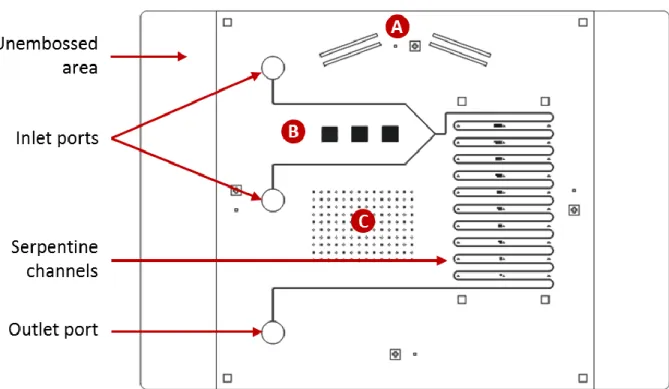
A custom microfluidic device was designed specifically as a test chip for the microfactory project [26]. The device is a simple micro-mixer with serpentine channels. Since flow at the micro-scale is laminar, mixing of two fluids depends primarily on diffusion. The longer the two fluids are next to each other, the more they will mix. The channel geometry for this design was chosen to be 50 μm wide and 40 μm deep and cover a 25 mm by 25 mm area. These are considered to be mid-sized channels for microfluidics, which made them a good starting point for this project. In addition to the main channels, the design includes a series of features that were designed to aid with registration, inspection, and testing the limitations of the embossing machine. The final pattern of the test chip can be seen in Figure 3-1. The project chose to focus on the embossing of PMMA. Future versions of the project will study the embossing of cyclic olefin copolymers (COCs), which are more widely used in the microfluidics industry. The tool is made out of a Zr-based bulk metallic glass, which is an amorphous metal. This allows for an extremely robust tool with a smooth embossing surface and precise features [27].
33
Figure 3-1: The final design of the micro-mixer device for the microfactory project. The two inlet
ports take two different fluids and mix them together along the serpentine channels via diffusion. (A), (B), and (C) are additional features of varying dimensions that were initially designed to help assess the embossing limits.
3.1.2 Hot Embossing
Several generations of hot embossing machines were developed before the current design was chosen. The earlier designs focused on understanding and improving the embossing process rather than optimizing the embossing equipment [28] [29]. Using information gathered from these projects, a new machine was developed to have a faster cycle time, lower cost, and smaller footprint [30]. This was the first machine to be implemented in the microfactory. It can be seen in the back left corner of the table in Figure 3-2.
34
Figure 3-2: The first version of the microfactory. A previous version of the hot embossing
machine is on the left. A robot arm for material handling is on the right. Previous versions of a bonding machine and dispenser for blank chips are located in the center [31].
The next and current hot embossing machine improved upon the previous version. In addition to being even smaller in size and having a faster cycle time (110 seconds), it also has several new alignment features for the tool as well as a linear variable differential transformer (LVDT) to measure displacement. A blank chip is placed on a platen between two thermal stacks that are embedded with ceramic heaters and cooling lines. The tool is mounted to the upper stack on a flexure that can be calibrated horizontally in the x-y plane to align with the pre-drilled inlet holes on the blank chips. The upper stack also has a thin sheet of rubber to account for small errors in parallelism between the tool and the chip. A pneumatic actuator at the bottom of the machine—combined with an air bearing—applies force directly upwards to push the plastic substrate against the stationary tool. The force is measured by a load cell and the displacement is measured by an LVDT. The plastic and the tool are brought into light contact while they are both heated to just above the glass transition temperature, Tg, of the material. Then, the machine
increases the pressure to fill the features of the tool. Next, the platens are cooled by pumping room temperature water through them. If the platens do not cool at similar rates (remaining
35
within approximately 10°C of each other) then significant warping of the chip can be observed. If the warping is too extreme, it can negatively affect the performance of other processes in the system. Finally, the pressure is released. During the cooling process, the plastic shrinks around the features of the tool. To release the chip from the tool, two thin tabs attached to the bottom platen hang over the un-embossed wings of the chip. When the platen lowers, the chip is demolded [7]. The final design is showed in Figure 3-3.
Figure 3-3: The current hot embossing machine design. Left: Photograph of machine with key
parts labeled. Right: Solid model of the machine [7].
The input parameters for this embossing machine are forming temperature, forming pressure, heating time, forming time, and cooling time. Cooling time is held constant, since the substrate needs to reach a certain temperature before it can demold successfully [9]. Heating time is also held constant because the material needs to reach its Tg. Currently, the forming time is also held
constant, but should be varied in the future to find the minimum cycle time. This leaves the forming temperature and forming pressure as the two main input variables for the machine. There are other variables that also need to be taken into account. Extruded PMMA sheets with a
36
material was 1.5 mm, but the chips could range anywhere from 1.1 mm to 1.8 mm (±20% variation). This affected the extent of heating through the plastic substrate, which would then affect the quality of embossing [7]. To avoid this problem, a new batch of PMMA blanks were injection molded. The variation in material thickness for the new blanks was reduced to ±1%. It was also found that the new material, despite still being PMMA, had a significantly higher Tg of
115°C.
3.1.3 Material Handling
Another important component of the microfactory is the material handling system. In order to have a fully automated factory, a method was needed for transporting the chips between the different stations. This positioning method also needed to be very precise, since the channels are only 50 μm wide. An Epson G10-85 robotic arm with 4 degrees of freedom was chosen to transport the chips. It has 25 μm repeatability in the horizontal plane and 10 μm repeatability in the vertical direction [32]. A custom end effector, shown in Figure 3-4, was designed to pick up the chips. The end effector needed a low profile to fit in between the hot embossing platens. Internal channels were added to draw a vacuum of 80 kPa (absolute pressure). Compliant rubber was added to the bottom surface to help improve the seal of the chips against the vacuum holes [33].
Figure 3-4: The underside of the original end effector [33].
The repeatability of the robot in the horizontal direction was improved from 25 μm to 11.3 μm by using a 3-pin alignment system [33]. These pins, shown in Figure 3-5, were mounted to
37
the lower platen of the hot embossing machine where the blanks are placed by the robot. The robot first placed the chip close to the pins. It then moved forward until the chip contacted the back pins and then moved to the right until the chip contacted the side pin.
Figure 3-5: The 3-pin alignment system reduced robot positioning variation from 25 μm to 11.3
μm [33].
The current robot end effector is based off this design but includes a few improvements. It now has two ports instead of one, which can be seen in Figure 3-6. This symmetrical design allows the robot to carry two chips at once. It can carry a blank chip in one port, remove an embossed chip from the hot embossing machine with the other port, and then immediately replace it with the blank chip. This significantly reduces the amount intermediate time between embossing cycles and improves the overall takt time of the microfactory. The current design also has a different vacuum hole pattern. The holes are located outside the embossed channel region on the edges of the chip. The region above the channels is milled away slightly. This prevents dust or dirt from accidentally transferring into the channels.
It was also noticed that the compliant rubber coating was causing the chips to occasionally stick to the end effector. To prevent this, the rubber was removed and a PMMA layer was used instead. The holes are still sealed well enough without the rubber. Lastly, a short “hook” was added to the front of each end effector. The robot picks up blank chips from a spring-loaded dispenser before it brings them to the hot embossing machine, and the vacuum pressure is not enough to overcome the pre-load of the dispenser. By adding the extra hook, the robot can pull the top chip free before turning on the vacuum to remove it from the dispenser. This hook is also useful in aligning chips later on in the system. If the robot pulls back on the chip before turning on the vacuum, the chip automatically straightens itself against the edge of the hook.
38
Figure 3-6: The current robot end effectors. Top: There are two symmetrical ports. Each port has
a short hook for manipulating the chips. Bottom: The vacuum holes were repositioned to avoid contacting the embossed channel region on the chip. The area between the holes is milled away. A simulated chip is added for clarity.
3.1.4 Bonding
After the microfluidic channels have been embossed, they need to be sealed before the chips are functional. This is currently one of the greatest difficulties in microfluidic device manufacturing. The first method that was attempted during the microfactory project was thermal bonding [34]. By heating up the embossed chip and a plastic cover plate and then applying pressure, the two pieces can be fused together for a strong seal. Unfortunately, reheating the channels often leads to deformation of the embossed features. One approach to minimizing feature deformation is to
39
use interfacial heating. Instead of heating the entire chip, only the surface is heated to just above the Tg. There is a temperature gradient throughout the rest of the chip, which helps prevent
over-heating. The use of radiative heating also allows the temperature at the surface to be controlled more rapidly than a traditional conductive heating system, since there is no residual heat when the heat source is turned off.
The final set-up used three 50 W halogen bulbs combined with an integrating sphere to created uniform light. The chip and cover plate were sandwiched between two pieces of glass above the light source and placed on an Instron machine that applied uniform pressure. The bonds were homogenous and optically clear. Sample images of the bonding process can be seen in Figure 3-7. The bonding region begins in the center of the chip and expands outwards.
Figure 3-7: Images of the chip and cover plate taken at different times during the bonding
process. The lighter areas indicate regions that have been bonded [34].
Unfortunately, there was still a significant amount of deformation in the channels. A variety of heating powers, pressures, and bonding times were tested. Out of the chips with all 10 channels fully bonded, most had final channel heights of less than 30 μm (compared to an initial 40 μm). The only sample with minimal deformation (final height of 37.7 μm) took 209 seconds to bond. This is nearly twice the desired cycle time of 110 seconds or less.
A new approach using adhesive tape as a cover plate to seal the channels was also explored briefly. While not all microfluidic designs are compatible with a non-homogenous fourth wall, it is still an accepted method. For the purposes of the microfactory project, this was an attractive solution because it would not alter the embossed channels and could be implemented quickly, which would enable the factory to start running earlier.
40
3.1.5 Inspection and Functional Testing
The final component of the microfactory project is a station for inspecting and functionally testing the microfluidic chips. The system needs to be able to detect if channels are under-formed so that it can signal the hot embosser to adjust its forming parameters accordingly. A high speed, high resolution inspection machine was developed to measure the chips [35]. It has comparable resolutions to a commercial interferometer with 0.5 μm horizontal and 1 μm vertical resolution, but is capable of processing a much higher rate of data points per second. It uses a high speed (500 fps) camera combined with motorized precision x-y stages to collect the data rapidly. It measures features by having the camera at an angle, as shown in Figure 3-8. Based on the depth of focus, it can determine the profiles of features in the image. Since the camera is at an angle, it is also able to image vertical side walls unlike other machines in its class. Commercial white light interferometers would take over 24 hours to image a 25 mm by 25 mm chip. This machine can measure the same area at a rate of 640,000 voxels per second. This corresponds to 65 minutes per chip at the highest resolution.
Figure 3-8: Left: Diagram of the high speed inspection with an angled camera. The different rows of
sensors in the camera focus on independent Z-heights. The camera moves horizontally, so multiple line scans can be taken in parallel. Right: Sample image of a channel compiled from the data taken with the inspection machine. It is able to detect the underfilled corners of the channels as well as defects in the features [35].
41
While this process produces very high quality and informative data which can be used to automatically detect small defects in the chips, it is not fast enough to be implemented in the microfactory system. It was decided that a simpler measurement within the given cycle time (110 seconds) would be more desirable from a process control standpoint. This led to the development of a series of functional testing machines that could use a quick test to measure whether or not the chips were functional.
One of the advantages to performing a functional test on the chips is that a bulk measure can be made to assess the overall geometry of the channels instead of relying on isolated measurements. Although functional tests for microfluidic devices are typically destructive, since the chip can no longer be used again, this is not important for the research factory. In an industrial application, the functional test could be performed once every hundred or so chips, while a less destructive inspection is performed every cycle.
The first generation of a functional testing system for the microfactory project used a constant-flow test designed to measure variations in pressure [36]. This test used a chip design different than the current micro-mixer. It used a series of short, straight 8 mm long channels with a variety of widths and depths (50-800 μm wide and 20-100 μm deep). The chips were sealed using a silicone gasket layer and two support platforms that were clamped together manually. The top support platform had pipe fittings to connect to a constant-flow syringe pump and a pressure gauge to the inlet and a mass scale to the outlet. The mass scale was used to calibrate the flow rate of the syringe pump. Results of these tests showed that it was possible to detect variation in channel geometries caused by changes in the embossing parameters. However, the testing process was very labor-intensive due to a complicated loading and unloading process, and there was too much fluid capacitance in the system. A long time was spent waiting for the tubing to expand and the air pockets in the pressure gauge to compress before fluid would start flowing, so testing times were on the order of 60 minutes. This was still too long for it to be implemented in the microfactory.
The next generation of the functional testing system, shown in Figure 3-9, was designed for the new micro-mixer chip pattern [37]. It used a constant-pressure driven test instead of a constant-flow rate driven test due to the difficulties with fluid capacitance in the previous system. This new system greatly reduced the amount of time required to test each chip (on the order of 2 minutes). To test the function of the micro-mixer chip, blue and yellow food dyes
42
were run through the channels where they would mix and turn green. This required sealing the chips first, so different adhesive tapes were tested using this system. Chips were placed by hand on a series of outlets connected to dye reservoirs with o-rings for a tighter seal. Two air cylinders on either side of the chip pulled down on an aluminum bar with a compliant rubber coating to clamp the chip in place. Two cylinders were chosen in this design because they were thought to be more symmetrical, but they were later found to be unnecessary. Once the chip was clamped, the flow was turned on. Both reservoirs were connected to the same line of pressurized air to ensure that the two fluids were at the same pressure. A Dino-Lite digital USB microscope was placed below the chip to capture images of the flow.
Figure 3-9: A pressure-driven functional test system for testing the micro-mixer chips. Blue and
yellow dyes connected to outlets were run through the channels of a chip which was clamped by two air cylinders. The clamp and flow pressures could be controlled by regulators [37].
43
This testing apparatus was a successful proof-of-concept for a functional test that could be integrated with the microfactory. It could successfully flow fluid through the channels within the desired cycle time, and it was small enough in size to fit on the table with the other equipment within reach of the robot arm. A variety of potential adhesive tapes for sealing the chips were also identified during the design of this system.
3.2 Areas of Improvement
The microfactory project had finally reached a point where it was feasible to integrate all of the different subsystems and create a working factory. The two biggest obstacles were in bonding and functional testing. A faster and more reliable method needed to be developed for bonding the chips. Without this, the chips could not be sealed and tested. Some initial tests with pressure sensitive adhesive tape had been promising, but the ideal tape still needed to be chosen. This also required the development of a fully automated machine that could apply the tape to the chips if the factory was to run autonomously. Since there were no commercially available machines for this specific purpose, a custom machine needed to be designed.
A proof-of-concept had been shown for the functional testing system, but the images recorded with this process were not a high enough quality. This required a redesign of the system to use higher quality optics and cameras to image the chips during the test. Also, the system needed to be automated in order to function with the rest of the microfactory. This included improving the alignment of the chips to allow for repeatable positioning.
Both the new bonding system and new functional testing system needed to be designed to be compatible with the rest of the microfactory. Previous generations had been designed to explore the processes, and they were not restrained by their size, control, or interface. These new systems needed to be able to fit on the tabletop factory with the hot embossing machine and robot arm. They needed to be accessible by the robot’s end effectors, and they needed to be able to communicate their current states with the robot. This became the motivation for the project described in this thesis.
44
3.3 Current Microfactory Project Objectives
The microfactory project has been running for several years, and its objectives have evolved based on the results of each individual project. While it started out as a project to study the process control of microfluidic devices, it later turned into a series of smaller in-depth projects to study the different processes of microfluidic device manufacturing. The focus has now shifted back to integrating all of the individual systems into a final capstone project. The current goals for the microfactory are as follows:
1. A production rate of 20-25 devices per hour (2.5 to 3 minute cycle time of the system).
2. Produce a continuous run of over 100 sealed and tested devices.
3. Determine the relationship between the test measurements of devices and the input parameters of the hot embossing machine.
3. Develop a strategy for closed-loop cycle-to-cycle process control.
The following chapters will describe the design of two machines—a taping machine and a functional testing machine—that are used to complete the microfactory system.
45
C
HAPTER
4
D
ESIGN OF A
T
APING
M
ACHINE
4.1 Design Specifications
The primary goal of this thesis project was to develop a reliable method to measure the quality of hot embossed chips in the microfactory. One of the possible methods for measuring quality was to perform functional tests of the microfluidic mixing devices. In order to perform tests, functional devices were required, so a sealing method for the embossed chips needed to be developed first. Previous work had investigated thermal bonding by applying a blank PMMA cover plate and heating it with the embossed chip to seal the channels. However, the channels started to melt back to their original state when enough heat was applied, causing the chips to no longer be functional. It was found that minimal channel deformation was possible, but not within the desired cycle time of less than 110 seconds (or the cycle time for the slowest machine in the system) [7]. Since the main purpose of the microfactory project as a whole was to study cycle-to-cycle process control in microfluidic device manufacturing rather than the mechanics of bonding methods, it was decided that a simpler, more reliable sealing method would be used instead. Laminate film bonding with adhesive tape seemed to be the most promising of the current microfluidic sealing methods for this project. While there are some devices which cannot function with non-homogenous walls, there are plenty of other applications that have been designed to work with adhesive tape [11]. It is inexpensive, quick to apply, and seals the micro-mixers well enough to be functionally tested.
Precisely handling and autonomously applying a non-rigid material, however, can be a challenging task. There are currently no off-the-shelf machines available for the needs of the project. This led to the development of a custom taping machine that could prepare embossed chips to be inspected and functionally tested by applying a layer of adhesive tape. The following design specifications were identified:
46
1. The tape must fully cover the channel and inlet region of the chip with at least a 2 mm border from the edge, to improve the seal and avoid leakage.
2. The tape must be strong enough to withstand 30 psi of fluid pressure for 2 minutes.
3. The adhesive must be thin enough that it does not clog the channels and obstruct the flow.
4. The adhesive’s backing needs to be stiff enough to keep the tape rigid and prevent it from deforming into the channels.
5. The tape must be optically clear, so chip features can be measured.
6. The adhesive must be uniform, so fluid doesn’t leak out into air bubbles between the adhesive.
7. Optional: The adhesive is biocompatible.
8. The chips do not require a manual processing step after taping to separate them from one another.
9. The taped chip can be picked up in a repeatable orientation to be placed precisely in the functional testing machine.
10. Full automation and compatibility with other machines in the microfactory project.
The following sections will describe the challenges and solutions that led to the final design of a taping machine for hot embossed microfluidic chips.
4.2 Design
4.2.1 Adhesive Tape Selection
First, a tape needed to be selected to seal the chips. There are a wide variety of tapes available to choose from. Some are heat-activated at a lower temperature than the glass transition temperature of PMMA, which would make thermal bonding more feasible. Others are UV curable. For this project, pressure-sensitive adhesive tapes were chosen because of their
47
availability and ease of application. Many tapes were sampled with a wide range of properties. From initial testing, it was found that adhesive strength, adhesive thickness, and plastic backing thickness were the most important parameters [37].
Several tapes did not have the strength to withstand flow pressures higher than 10 psi before leaks began to form around either the channel area or the inlet area. The more successful tapes could withstand over 35 psi, which is far higher than the maximum pressure required for testing chips (10-20 psi). Adhesive thickness also played a large role in tape selection. For example, 3M 600 tape has an adhesive thickness of 37.5 μm. Since the channel height is only 40 μm, the adhesive ended up filling most of the channel and blocking flow. It was found that tapes with adhesive thicknesses less than 20 μm were ideal. Adhesive backing thickness is also important. Tapes with very thin backings were able to deform into channels too easily. Therefore, a more rigid backing of 50 μm or higher is preferable.
Some other important factors include uniformity of the adhesive to keep the channels sealed without leakage and clarity to allow measurements of the features to be taken through the tape. One of the more successful tapes was 3M 810 Scotch Magic Tape, which was able to withstand up to 30 psi of flow pressure. Unfortunately, it has a slightly hazy appearance, shown below in Figure 4-1, making it difficult to take measurements within the channels. Another promising tape was product 92712 from Adhesives Research, Inc. This is a medical grade tape, which is an additional advantage, with a thin 17.5 μm adhesive thickness. Unfortunately, it is only available as a double-sided tape, which does not work for this project.
48
The most promising tape for sealing these devices was product 62551 from Tesa Tape, Inc. The tape is biocompatible and was originally designed for microfluidic applications with channels that were much wider at 200 μm. The adhesive is very thin to avoid filling channels and the backing layer is rigid enough to avoid collapsing into the channels.3 This tape can easily withstand pressures up to 35 psi (higher pressures have not been tested) for extended periods of time, and it is also visually clear, as seen below in Figure 4-2.
Figure 4-2: A micrograph of a chip sealed with Tesa Tape 62551.
The surfaces of channels sealed with Tesa Tape 62551 were measured using a Zygo white light interferometer to check for signs of tape sinking into channels4. The profile of tape covering a well-embossed channel is shown on the left of Figure 4-3. The channel is barely visible, but most of the height data varies over less than 0.4 μm. The profile of tape covering a poorly-embossed channel is shown on the right of Figure 4-3. The scale is exaggerated, since the height difference is only 1.6 μm, but there is still evidence that it is possible for the tape to sink into the channels if they are poorly formed enough.
3 This tape is still under development, so further details will not be published, per their request. 4 Zygo NewView 5000
![Figure 2-4: Application of a UV-curable adhesive resin using capillary action to prevent clogged channels [13]](https://thumb-eu.123doks.com/thumbv2/123doknet/14733097.573494/25.918.282.631.113.469/figure-application-curable-adhesive-capillary-prevent-clogged-channels.webp)