HAL Id: hal-00018243
https://hal.archives-ouvertes.fr/hal-00018243
Submitted on 23 May 2014
HAL is a multi-disciplinary open access
archive for the deposit and dissemination of
sci-entific research documents, whether they are
pub-lished or not. The documents may come from
teaching and research institutions in France or
abroad, or from public or private research centers.
L’archive ouverte pluridisciplinaire HAL, est
destinée au dépôt et à la diffusion de documents
scientifiques de niveau recherche, publiés ou non,
émanant des établissements d’enseignement et de
recherche français ou étrangers, des laboratoires
publics ou privés.
Spectroscopy of electronic states in InAs quantum dots
grown on In(x)Al(1-x)As/InP(001)
F. Fossard, A. Helman, G. Fishman, F. H Julien, J. Brault, M. Gendry,
Emmanuel Peronne, Antigoni Alexandrou, S. E Schacham, G. Bahir, et al.
To cite this version:
F. Fossard, A. Helman, G. Fishman, F. H Julien, J. Brault, et al.. Spectroscopy of electronic states in
InAs quantum dots grown on In(x)Al(1-x)As/InP(001). Physical Review Letters, American Physical
Society, 2004, 69, pp.155333. �10.1103/PhysRevB.69.155333�. �hal-00018243�
Spectroscopy of the electronic states in InAs quantum dots grown on In
xAl
1ÀxAsÕInP„001…
F. Fossard,*A. Helman, G. Fishman, and F. H. Julien
Institut d’Electronique Fondamentale, UMR 8622 CNRS, Universite´ Paris XI, 91405 Orsay Cedex, France
J. Brault and M. Gendry
Laboratoire d’Electronique-LEOM, UMR 5512 CNRS, Ecole Centrale de Lyon, 69134 Ecully Cedex, France
E. Pe´ronne and A. Alexandrou
Laboratoire d’Optique et Bioscience, UMR 7645 CNRS, Ecole Polytechnique-Ensta, 91128 Palaiseau Cedex, France
S. E. Schacham
Department of Electrical and Electronical Engineering, College of Judea and Samaria, Ariel 44837, Israel
G. Bahir and E. Finkman
Department of Electrical Engineering and Solid State Institute, Technion, Haifa 32000, Israel ~Received 13 May 2003; published 29 April 2004!
We have investigated optical properties of high-density InAs self-assembled quantum dots ~QDs! in an InxAl12xAs matrix, lattice matched to an InP ~001! substrate. The weak lattice mismatch (;3%) results in a 90% coverage of the InxAl12xAs surface with InAs QDs. By means of interband and intraband spectroscopies crossed with atomic force microscopy ~AFM! measurements, we have determined that the InAs QDs optical properties depend on the deposited amount of InAs. Photoinduced absorption spectroscopy has been used to investigate midinfrared intraband absorptions. For three monolayers ~ML! InAs deposit thickness, just above two-dimensional ~2D!/3D growth mode transition ~2.5 ML!, the islands form as isolated elliptical dots elon-gated along the@11¯0# direction and exhibit intraband resonances polarized either along the @110# or the @11¯0#
direction. For thicker deposition (.3 ML), InAs islands form chains of elliptical dots along the @11¯0# direc-tion where the quantum confinement is lost, resulting in a quantum-wire-like behavior. In this paper, we also report on photoluminescence and photocurrent spectroscopies, in order to get insight into the InAs/InxAl12xAs island band structure. These experimental results are in good agreement with that of a multiband k•p model. DOI: 10.1103/PhysRevB.69.155333 PACS number~s!: 78.67.Hc, 78.55.Cr, 73.21.La, 07.57.Ty
I. INTRODUCTION
Quantum dots ~QDs! are of key interest for applications to infrared ~IR! optoelectronics such as IR photodetectors,1 IR lasers,2 or basic single-photon emission devices.3The elec-tronic and optical properties of zero-dimensional ~0D! semi-conductors are fundamentally different from those of 1D, 2D, and bulk semiconductors. The three-dimensional con-finement of the carriers results in an atomlike density of states d(E). The discretization of the density of states was predicted to slow down the interlevel relaxation of the carriers.4This so-called ‘‘phonon bottleneck’’ effect,5which has been recently revisited in terms of polaron relaxation due to the strong electron-phonon coupling in QDs,6 – 8 can im-prove the quantum efficiency of unipolar devices such as quantum dot infrared photodetectors9 ~QDIP! or quantum
cascade lasers.10 Moreover, the in-plane confinement of the carriers allows the intraband absorption or the emission of photons at normal incidence, which is forbidden in quantum wells. In order to obtain a better efficiency, a high density of dots is required as well as a large oscillator strength of the intraband optical transition. In previous works, we showed that the self-organized growth in the InAs/In0.52Al0.48As/InP(001) system results in a high density
of InAs quantum islands11 and that strong intraband reso-nances take place at wavelengths of 14 –15mm with a polar-ization in the layer plane along the @110# axis.12
In this paper, we report on intraband spectroscopy of self-organized InAs QDs grown on In0.52Al0.48As/InP(001). We
show that the quantum islands morphologies and their asso-ciated physical properties can be varied, according to the amount of InAs deposited. When the thickness of InAs is equal to three monolayers ~ML!, we obtain isolated QDs elongated in the@11¯0# direction. When the InAs thickness is
increased by only 0.5 ML, QDs connect and form linear chains along the same @11¯0# direction. The quantum
struc-tures have a different optical behavior related to their iso-lated or connected nature. In isoiso-lated dots, we present evi-dence of the quantum confinement of the carriers in the @110# and @11¯0# directions. We then show that the confinement
along the@11¯0# direction is lost in the chains of dots and that
intraband resonances are narrower than in isolated dots. This indicates a smaller size dispersion of the chains of dots. In order to reconstruct the energy diagram of the dots, photo-current spectroscopy of the dots has been performed to as-sess the ground-state energy. We also present a two-band
II. SAMPLE GROWTH
The four samples, labeled A to D, studied in this work
~see Table I! were grown at 525 °C on semi-insulating InP
substrates using solid-source molecular-beam epitaxy. All samples consist in an In0.52Al0.48As (InxAl12xAs) buffer
layer lattice matched to InP, an active region containing 10 planes of InAs QDs separated by 50-nm-thick InxAl12xAs
spacer layers, and a 300-nm InxAl12xAs cap layer. For InAs/InxAl12xAs QDs, it is possible, by the control of the
InAs surface reconstruction @(234) or (231)] and the InxAl12xAs surface preparation ~growth interruption time,
under arsenic flux, before the InAs growth!, to obtain either wires or elongated dots.11,12 In this work, the InAs growth conditions @growth temperature and arsenic pressure favor-ing (231) reconstruction# and the InxAl12xAs surface
preparation ~growth interruption time of 600 s! were chosen to favor the formation of InAs elongated dots. Our attention is especially focused on the deposited amount of InAs. For samples A and B (C and D), the thickness of InAs deposited in each plane is 0.9 nm ~1.05 nm! corresponding to 3 ~3.5! ML. Sample B contains lattice-matched In0.53Ga0.47As
con-tact layers which were grown at the bottom ~500 nm n-doped at 831018cm23) and the top ~500-nm n-doped at 1018 cm23) of the structure for photocurrent spectroscopy
purposes. For this sample, the InxAl12xAs spacer layers were
d-doped at the center with silicon to achieve a sheet carrier density of 531011 cm22. For sample D, d doping is
per-formed 15 nm below and above the InAs layer to achieve a sheet carrier density of 131012 cm22.
III. ISOLATED ELONGATED DOTS
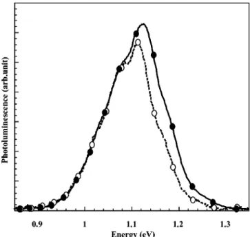
Figure 1 shows the photoluminescence ~PL! spectrum of sample A at 77 K. The optical excitation is provided by an argon laser. The low excitation spectrum '40 W cm22
~dot-ted curve! reveals a structured peak at 1.1 eV with a full width at half maximum ~FWHM! of 124 meV, reflecting the size dispersion of the dots. Weber et al. showed that the structure of the PL is mainly related to various dot heights corresponding to an integer number of ML and also to ex-cited states.13
Under intense excitation '1.5 kW cm22, the PL
spec-trum ~solid curve! reveals that the high-energy side of the peak increases with the excitation intensity. The PL FWHM is 139 meV, which is 11% larger than that under low excita-tion condiexcita-tions. The optical excitaexcita-tion provides electron-hole pairs in the dots and in the barriers. The filling of the dots is a result of complex processes which involve transport and
capture of the carriers. However, at high excitation, the ground state of the dots is full and the increase of the high-energy side of the peak can be attributed to optical recombi-nation between excited states of the dots.14 –16This last result demonstrates the dotlike behavior of this type of InAs is-lands. The global broadening of the PL spectrum, at high energy, is an indication of the filling of either the excited states of the large dots or the ground state of the small dots. Since intraband transitions are polarized along the con-finement direction, we expect to observe intraband absorp-tions for both in-plane polarizaabsorp-tions ~@110# and @11¯0#).
Thus, it is difficult to perform standard transmission mea-surements due to the lack of ideal reference. Intraband ex-periments were first performed using photoinduced absorp-tion ~PIA! spectroscopy. The sample is optically excited by a chopped argon laser to generate electron-hole pairs. The re-sulting intraband absorption is probed using a Fourier trans-form infrared spectrometer operating in step-scan mode and using standard lock-in techniques.17 The density of carriers generated by the excitation (10921010 cm22) is negligible compared to the intentional doping. As the reference spec-trum is provided by a transmission of the same sample with-out optical excitation, this method does not require a sepa-rated undoped sample as a reference. This very sensitive method allows the observation of absorption as weak as 1026.
Figure 2~a! shows the PIA spectra of sample B at normal incidence at 77 K for two in-plane polarizations. The top InxGa12xAs layer of the sample was chemically etched to
reduce free-carrier absorption and to allow optical excitation of the active layer. The @110# polarized spectrum shows a narrow absorption at 87 meV with a FWHM of 13 meV. A second peak, ten times smaller, occurs at 120 meV with a FWHM of about 30 meV. The @11¯0# polarized spectrum
exhibits two absorptions. On the low-energy side, one can
TABLE I. Growth parameters for the four samples studied in this work.
Sample n doping (cm22) InAs thickness ~nm!
A No 0.9
B 531011 0.9
C No 1.05
D 131012 1.05
FIG. 1. 77 K photoluminescence spectra of sample A at low excitation ~dotted curve! and high excitation ~solid curve!.
FOSSARD et al. PHYSICAL REVIEW B 69, 155333 ~2004!
see the onset of an absorption at 80 meV with a FWHM of the order of 20 meV. The sharp notches near 78, 82, and 86 meV are due to two-phonon absorptions in the InP substrate. The 80-meV peak is not related to free-carrier absorption because it is only observed for one polarization. Note that a second peak, at higher energy, occurs at 108 meV with a FWHM of about 30 meV. Figure 2~b! shows the PIA spectra at normal incidence of sample B at 300 K. With increasing temperature, each transition is redshifted by 2–3 meV, which is typical of interlevel transitions.18 For both polarizations, the relative intensity of the high-energy absorptions com-pared to the low-energy absorptions increases by 40%. This result has been confirmed by normal incidence transmission measurements at 77 and 300 K. This reveals that the high-energy transitions occur between excited states of the dots. With the temperature increase, the first excited states ( p states! are filled with more carriers. Thus, the absorption from the ground state is reduced while the absorption from excited p states is increased. As the dots have a preferential
orientation, we can attribute the observed low-energy reso-nances in @110# (@11¯0#) to transitions from the ground state s to an excited state p with an envelope wave function with
one node along the @110# (@11¯0#) axis. High-energy
absorp-tions can be related to transiabsorp-tions from a p state with one node along the @110# (@11¯0#) axis to a higher excited stated
with two nodes along the @110# (@11¯0#) axis.
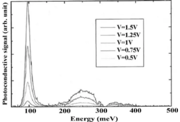
Additional photocurrent ~PC! experiments19 were per-formed at normal incidence ~front illumination! on sample
B. PC measurements are important for QDIPs applications
and also provide more insight since we observe more transi-tions than in absorption measurements. Figure 3 shows the photocurrent spectrum as a function of the energy of the incident radiation for different bias applied to the structure. The spectra exhibit two main structures which behave differ-ently. On the high-energy side, we can notice a broad peak at 250 meV. The peak of the photoconductive current depends linearly on the applied bias which is typical of bound to continuum transitions. Thus, it reveals that the ground state of the dots in sample B lays 250 meV below the continnum.20 On the low-energy side, a structure appears at 95–100 meV and has a superlinear dependence with the bias. Such behavior is expected for a bound to bound transition since the tunneling probability of the carriers from the upper bound level into the continuum increases as the barrier be-comes more slanted. We can easily link this peak to the in-tense absorptions observed at the same energy in PIA experi-ments. Since this transition is followed by tunneling, its amplitude is thus reduced, and becomes comparable to that of the higher energy in spite of its very large oscillator strength.
IV. CHAINS OF ELONGATED DOTS
Figure 4 shows the photoluminescence spectra of sample
C at 77 K for two excitation intensities. At low excitation ~dotted curve!, the luminescence is peaked at 1.03 eV with a
FWHM of 117 meV. It should be noticed that the PL occurs at a lower energy with respect to isolated dots. This energy reduction is related to the increased dot height, as expected from the larger amount of the InAs deposited in this sample.
FIG. 2. Photoinduced absorption spectra of sample B at normal incidence for two orthogonal in-plane polarizations. Absorptions were probed at 77 K ~upper graph! and 300 K ~bottom graph!.
FIG. 3. Normal incidence photocurrent spectra of sample B at 15 K as a function of the incident light energy for several biases applied to the structure.
We estimate that, in this sample, the dots are about 1 ML higher than in sample B.
The solid curve of Fig. 4 shows the PL spectrum of sample C under high excitation. The shape of the PL peak is basically unchanged with increasing excitation density. In contrast to the isolated dots, the chains of dots do not exhibit hot photoluminescence from the excited states. This behavior suggests a quantum-wire-like type of confinement. Indeed, in a quantum wire, even if the density of state is peaked at k
50, there is still room for carriers in the ground subband.
This point clarifies the ambiguous behavior of the InAs QDs grown on InxAl12xAs already mentioned by Weber et al.13
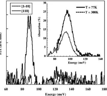
Figure 5 shows the 77 K PIA spectra of sample C at normal incidence, respectively, for light polarized along the
@110# and @11¯0# directions of the layer plane. The @110#
polarized spectrum reveals an intense and narrow absorption at 90 meV with a small FWHM of 7.5 meV. This resonance can be attributed to the intraband transition between the ground state and the first excited state related to the confine-ment of the electron along @110#. Within expericonfine-mental accu-racy, no absorption is observed for a polarization along the
@11¯0# direction in the investigated spectral range.
The inset of Fig. 5 shows the absorption spectra at normal incidence of the n-doped sample D as a function of tempera-ture. At 77 K, the absorption reaches the record value of 26% at 95 meV ~12.8mm! with a 16 meV FWHM. According to Weber et al., it is clear that the observed transition occurs in the conduction band. The absorption of one plane A can be approximated by
A512e2NpsrS
with s the absorption cross section and rS the 2D carrier
density. We deduce the oscillator strength f of the transition from21
f 5nc«e02m\0sz
with the refractive index n of InAs, the speed of light c, the electric constant «0, the electronic mass m0, the elementary
charge e, and the FWHM of the transition z. The obtained value is of the order of 21. Note that this large value is likely to be underestimated because we assumed that all electrons are trapped in the dots. One should also take into account the band bending in heavily doped heterostructures.d doping in the barrier creates a depletion region and band bending which may reduce the probability of electrons to be localized on a confined level.
The inset of Fig. 5 also shows that the integrated absorp-tion drops by 32% when the temperature is increased from 77 K to room temperature. Populations of the upper and ground states are estimated, as a first approximation, assum-ing a 1D-subband effective-mass model. The Fermi level «F
verifies N1D5
E
0 ` r~ « ! 1 11expS
«2«k F BTD
d«,wherer~«! is the density of state in a wire, N1Dis the density
of carriers in a wire, and kB is the Boltzmann constant. We
deduce the population of the two levels from this calculus and evaluate the absorption. Results confirm that the absorp-tion is expected to drop by 30% when the temperature is increased from 77 to 300 K. Intraband spectroscopy confirms the wirelike behavior of the chains of elongated dots since no absorption is observed in the @11¯0# direction. The
connec-FIG. 4. 77 K photoluminescence spectra of sample C at low excitation ~dotted curve! and high excitation ~solid curve!. The inset shows a typical AFM image of an uncapped sample.
FIG. 5. Normal incidence photoinduced absorption spectra of sample C, at 77 K, for polarizations @110# and @11¯0#. The inset
shows the absorption of sample D, at normal incidence, as a func-tion of the photon energy at 77 and 300 K.
FOSSARD et al. PHYSICAL REVIEW B 69, 155333 ~2004!
tion of the dots along the big axis@11¯0#, as indicated by the
atomic force microscopy ~AFM! image, induces the forma-tion of short wires.
V. MODEL AND ENERGY DIAGRAM
At the vicinity of k50, the band structure of a semicon-ductor can be approximated by a parabolic dispersion curve but in the range of a few percent of the Brillouin zone only. The nonparabolicity becomes stronger in narrow-gap semi-conductors such as InAs. Therefore, it is inaccurate to use a one-band model to simulate the energy structure of the iso-lated elongated dot. Since we are mainly interested in the electron states, a good approximation of the conduction band is required. First of all, we calculate the bulk dispersion of the InAs with the eight-band matrix of Pidgeon and Brown22 using the Luttinger parameters given by Boujdaria et al.23 We then use a two-band k•p matrix to fit the correct conduc-tion band within the first 10% of the Brillouin zone.
Since the exact shape of the dots is unknown, as well as their large size dispersion, a few approximations were made to simplify the calculations. Variable separation was used for
X, Y , and Z. The shape of the truncated pyramidal dot can
be approximated by a rectangular box with the same volume. The energy of the electrons is assumed to be the sum of the confinement in three quantum wells representing the confine-ment along the three axes of the dots: @110#, @11¯0#, and @001#.
We chose to describe each band with a base of sine func-tions, as described in Ref. 24, which simplifies the calcula-tion of the derivatives and integrals in each matrix element. In order to obtain a good description of the energy, the model requires quite a large base with each band described by 30 sine functions. This procedure leads to an accuracy of about 1 meV. For the two-band model described above, the size of the matrix is then 60360.
Results of the calculation are illustrated in Fig. 6. The
curves show the calculated energy transitions E1 – 2and E2 – 3
depending on the confinement direction of the plane. Note that for a length of 180 Å, E1 – 2 and E2 – 3 are calculated,
respectively, as 80 and 108 meV; and for a width of 164 Å,
E1 – 2 and E2 – 3 are calculated, respectively, as 91 and 118 meV. Moreover, we calculated the position of the electronic ground state of the dots and we obtained values between 220 and 320 meV. Once again, the calculated value is close to the experimental value. Equivalent values have been calculated using an eight-band model. It demonstrates that the two-band model allows a good description of the electronic states.
The good agreement between the calculation and the ex-periments allows us to construct the energy diagram of the dots. The resonances observed at low energies in both polar-izations are attributed to intraband transitions between the s ground state of the dots and the first p excited state ~enve-lope wave function with one node in the layer plane! relative to the confinement along the @110# and @11¯0# directions.
Moreover, the high-energy absorption peaks can be attributed to transitions starting from p states to d states ~two nodes in the layer plane!.25 Figure 7 summarizes the energy diagram of the isolated elongated dots. We chose to label the elec-tronic state with three quantum numbers representing the number of nodes in the three directions X, Y , and Z which correspond to crystallographic directions @11¯0#, @110#, and @001#, respectively.
VI. CONCLUSION
In this paper, we report on optical spectroscopy of InAs quantum islands grown on InxAl12xAs lattice matched to
InP~001!. Samples containing different types of InAs islands
FIG. 6. Calculated energies of the E12and E23intraband transi-tions as a function of the in-plane dimension of the dot.
FIG. 7. Energy diagram of the isolated elongated dots. Each level is labeled with three quantum numbers X, Y , and Z indicating the number of nodes along the@11¯0#, @110#, and @001# direction,
have been studied by photoluminescence, infrared spectros-copy, and photocurrent spectroscopy. All samples show strong midinfrared intraband absorptions at normal inci-dence. We have shown that the optical behavior of the is-lands is affected by the amount of InAs deposited. When the thickness of InAs ~3 ML! is just above the 2D/3D transition
~2.5 ML!, the islands behave like quantum dots. The
obser-vation of giant s- p resonances in the 12–20mm region and weaker p-d absorptions in the 8 –12-mm region has con-firmed the three-dimensional confinement of the islands. Added to photocurrent spectroscopy, these results have al-lowed the reconstruction of the energy diagram of the dotlike InAs islands.
On the other hand, when the amount of InAs deposited reaches 3.5 ML, the discrete signature disappears and the InAs islands behave like quantum wires. This effect is attrib-uted to the connection of the dots along the @11¯0# axis.
Moreover, the optical spectroscopy of these strings reveals a weaker size dispersion related to the FWHM of the spectra. Infrared spectroscopies have shown that the intraband ab-sorption reaches a record value of 26% for 10 planes of
n-doped (1012cm22) chains of elongated dots. The FWHM
of the intraband absorption is as small as 7.5 meV at 13.5
mm in undoped samples.
We have shown that the energy structure of the isolated elongated dots can be described by a simple two-band k•p model which takes into account the strong nonparabolicity in InAs. Calculations show good agreement with the experi-mental data.
ACKNOWLEDGMENT
The authors would like to thank J. P. Leburton for fruitful discussions.
*Corresponding author. Electronic address: frederic.fossard@ ief.u-psud.fr
1B. F. Levine, J. Appl. Phys. 74, R1 ~1993!.
2Y. Arakawa and H. Sasaki, Appl. Phys. Lett. 40, 939 ~1982!. 3
A. Imamoglu and Y. Yamamoto, Phys. Rev. Lett. 72, 210 ~1994!. 4U. Bockelmann and G. Bastard, Phys. Rev. B 42, 8947 ~1990!. 5H. Benisty, C. M. Sotomayor-Torre`s, and C. Weisbuch, Phys.
Rev. B 44, 10 945 ~1991!.
6S. Hameau, Y. Guldner, O. Verzelen, R. Ferreira, G. Bastard, J. Zeman, A. Lemaıˆtre, and J. M. Ge´rard, Phys. Rev. Lett. 83, 4152
~1999!.
7S. Hameau, J. N. Isaia, Y. Guldner, E. Deleporte, O. Verzelen, R. Ferreira, G. Bastard, J. Zeman, and J. M. Ge´rard, Phys. Rev. B 65, 085316 ~2002!.
8O. Verzelen, R. Ferreira, and G. Bastard, Phys. Rev. B 62, 4809
~2000!.
9E. Finkman, S. Maimon, V. Immer, G. Bahir, S. E. Schacham, O. Gauthier-Lafaye, S. Herriot, F. H. Julien, M. Gendry, and J. Brault, Physica E ~Amsterdam! 7, 139 ~2000!.
10C. Becker, C. Sirtori, O. Drachenko, V. Rylkov, D. Smirnov, and J. Leotin, Appl. Phys. Lett. 81, 2941 ~2002!.
11J. Brault, M. Gendry, G. Grenet, G. Hollinger, J. Olivares, B. Salem, T. Benyattou, and G. Bremond, J. Appl. Phys. 92, 506
~2002!.
12F. Fossard, F. H. Julien, E. Pe´ronne, A. Alexandrou, J. Brault, and M. Gendry, Infrared Phys. Technol. 42, 443 ~2001!.
13A. Weber, O. Gauthier-Lafaye, F. H. Julien, J. Brault, M. Gendry, Y. De´sieres, and T. Benyattou, Appl. Phys. Lett. 74, 413 ~1999!.
14S. Fafard and R. Leon, Phys. Rev. B 52, 5752 ~1995!.
15M. J. Steer, D. J. Mowbray, W. R. Tribe, M. S. Skolnick, M. D. Sturge, M. Hopkinson, A. G. Cullis, C. R. Whitehouse, and R. Murray, Phys. Rev. B 54, 17 738 ~1996!.
16
B. Salem, T. Benyattou, G. Guillot, C. Bru-Chevallier, G. Bremond, C. Monat, G. Hollinger, and M. Gendry, Phys. Rev. B 66, 193305 ~2002!.
17S. Sauvage, P. Boucaud, F. H. Julien, J.-M. Ge´rard, and J.-Y. Marzin, J. Appl. Phys. 82, 3396 ~1997!.
18P. Von-Allmen, M. Berz, G. Petrocelli, F. Reinhart, and G. Har-beke, Semicond. Sci. Technol. 3, 1211 ~1988!.
19E. Finkman, S. Maimon, V. Immer, G. Bahir, S. E. Schacham, F. Fossard, F. H. Julien, J. Brault, and M. Gendry, Phys. Rev. B 63, 045323 ~2001!.
20S. E. Schacham, G. Bahir, E. Finkman, F. H. Julien, F. Fossard, J. Brault, and M. Gendry, Infrared Phys. Technol. 44, 509 ~2003!. 21F. H. Julien and P. Boucaud, in Optical Intersubband Absorption
and Emission in Quantum Structures, Vol. 344 of NATO
Advanced Study Institute, Optical Spectroscopy of
Low-dimensional Semiconductors, Ankara, Turkey, September 1996,
edited by G. Abstreiter ~Kluwer Academic, Dordrecht, 1997!, pp. 41– 61.
22C. R. Pidgeon and R. N. Brown, Phys. Rev. 146, 575 ~1966!. 23K. Boujdaria, S. Ridene, and G. Fishman, Phys. Rev. B 63,
235302 ~2001!.
24G. Fishman, Phys. Rev. B 52, 11 132 ~1995!.
25F. Fossard, A. Helman, F. H. Julien, M. Gendry, J. Brault, E. Pe´ronne, A. Alexandrou, S. E. Schacham, and E. Finkman, Physica E ~Amsterdam! 17, 82 ~2003!.
FOSSARD et al. PHYSICAL REVIEW B 69, 155333 ~2004!