Design of a 3-Dimension FPGA
by
Payam Lajevardi
B.A.Sc., Electrical Engineering, University of British Columbia
Submitted to the Department of Electrical Engineering and Computer
Science
in partial fulfillment of the requirements for the degree of
Master of Science in Electrical Engineering and Computer Science
at the
MASSACHUSETTS INSTITUTE OF TECHNOLOGY
July 2005
@
Massachusetts Institute of Technology 2005. All rights reserved.
A uthor ...
Department of Electrical Engineering and domputeo Science
July 29, 2005
Certified by ...
Anantha P. Chandrakasan
Professor of Electrical Engineering
Thesis Supervisor
Accepted by ...
...
Arthur C. Smith
Chairman, Departmental Committee on Graduate Students
BARKER
IASSACHUSETTS INST EOF TECHNOLOGY
Design of a 3-Dimension FPGA
by
Payam Lajevardi
Submitted to the Department of Electrical Engineering and Computer Science on July 29, 2005, in partial fulfillment of the
requirements for the degree of
Master of Science in Electrical Engineering and Computer Science
Abstract
The interconnect delay in the new generations of integrated circuits imposes a signif-icant limitation on the performance of ICs. 3-Dimensional integration of integrated circuits had been proposed to improve the interconnect delay. In this research, the effect of 3-D integration on the delay and power of FPGA chips is analyzed. Different physical partitioning of FPGAs is proposed for 3-D integration and one is analyzed in detail. The size of 3-D FPGAs differs from the size of 2-D FPGAs because of the overhead of 3-D connections and different connectivity in switch blocks. Layout of
2-D and 3-D FPGAs is prepared to compare their size. To compare 3-D and 2-D
FPGAs properly, two basic routability metrics are proposed to compare the routabil-ity of 3-D and 2-D circuits. Then, the delay of a 2-D and a 3-D FPGA with the same routability is compared. It is shown that 20%-29% delay improvement can be achieved by using a 3-D FPGA.
In addition, the power consumption of 3-D FPGAs is analyzed. It is shown that if the supply voltage and the operating frequency of a 3-D FPGA are held to be the same as a 2-D FPGA, 17%-22% power improvement can be achieved. However, 3-D FPGAs can run faster since their delay is improved as well. If the delay improvement is traded off for more power saving by lowering the supply voltage, 35%-39% power improvement can be expected.
Finally, to reduce the magnitude of supply current required for an integrated circuit, the method of stacking logic circuits is analyzed. This method requires level conversion between different supply domains. In this research, the architecture of several level converters are described and their delays are compared.
Thesis Supervisor: Anantha P. Chandrakasan Title: Professor of Electrical Engineering
Acknowledgments
I would like to thank Professor Anantha Chandrakasan for his support. I enjoyed
the learning opportunity in his research group under his supervision and guidance. I would also like to thank other members of Anantha group whose valuable input have enhanced my insight in my research. In particular, I would like to thank Dr. Young-Su Kwon, Frank Honore, Benton Calhoun, Raul Blazquez and Daniel Finchelstein for their help. In addition, I would like to thank Lincoln Lab Corporation, which provided us with fabrication facilities, and Professor W. Rhett Davis and his research group in North Carolina State University (NCSU) for their CAD support for 3-D fabrication. Finally, I would like to thank my parents, Soraya Mohammadi and Hosein Lajevardi, and my brother, Pedram Lajevardi, for their support and love.
Contents
1 Introduction
1.1 Overview of FPGAs . . . . 1.2 Overview of 3-D Integrated Circuits . . . .
2 Analysis of 3-D FPGAs
2.1 Programming an FPGA chip.
2.2 Possible 3-D Architectures . .
2.3 Block Diagram . . . . 2.4 Wire Length Estimation . . .
2.5 Delay Analysis . . . . 2.6 Power analysis . . . . 3 Fabricated Chip
3.1 Hardware Design of the Fabricated Chip . . . .
3.2 Synthesis and Layout of the fabricated chip . . . .
4 Stacking Logic Blocks
4.1 Motivation for Stacking Logic Blocks . . . . 4.2 Required Circuits for Stacking Logic Blocks . . . . 4.3 Basic Level Converter for Stacked Logic . . . .
4.4 A Level Converter with a Pulse Generator at the Output . . . . 4.5 A Level Converter with Pre-charge . . . . 4.6 Domino Level Converter . . . .
13 14 16 19 . . . . 19 . . . . 20 . . . . 25 . . . . 28 . . . . 33 . . . . 38 45 45 48 53 53 55 56 58 59 60
5 Conclusions 63 A Smooth Bell-Shape Histogram 65
List of Figures
1-1 A General Block Diagram of Field Programmable Gate Arrays (FPGA). 14
1-2 Switch block pins with different switch flexibility. . . . . 15
2-1 General Block Diagram of a 3-D FPGA. . . . . 22
2-2 A 3-D FPGA Architecture with one Configuration Layer and one Ac-tive Layer. . . . . 23
2-3 A 3-D FPGA Architecture with Switch Block Split in two Active Layers. 24 2-4 Programmable Logic Block (PLB). . . . . 25
2-5 The Block Diagram of Configurable Logic Block. . . . . 26
2-6 The Block Diagram of InputMUX. . . . . 27
2-7 The Block Diagram of 2-D Switch Block. . . . . 28
2-8 The Block Diagram of 3-D Switch Block. . . . . 29
2-9 The Block Diagram of a Tile. . . . . 30
2-10 The Area of Tile Vs. the Channel Width of Interconnect. . . . . 31
2-11 The Area Penalty in 3-D Tiles Comparing to 2-D Tiles due to Inter-Layer Via and 3-D Switch Block as a Function of the Channel Width of Interconnect. ... ... .. 32
2-12 The Length of Interconnect Vs. the total number of wires connected to the switch block. . . . . 33
2-13 Different Segments of a Connection from a FF in One Tile to Another FF in an Adjacent Tile. . . . . 35
2-14 The Delay Histogram of Point-to-Point Connections in the 2-D FPGA and the 3-D FPGA with Transmission Gates as a Switch Cell. ... 37
2-15 Possible Options for a Switch Cell. . . . . 38
2-16 The Delay Histogram of Point-to-Point Connections in the 2-D FPGA and the 3-D FPGA with Tri-State Buffers as a Switch Cell. . . . . 39
2-17 The Delay of Tri-State Buffer vs. Vdd. . . . . 40
2-18 Energy Consumption of MUX vs. Vdd. . . . . 41
2-19 Energy Consumption of Different Parts of a Tile Vs. Vdd. . . . . 42
2-20 Histogram of Energy Consumption of All Point-to-Point Connections without Scaling Supply Voltage in 3-D. . . . . 43
2-21 Histogram of Energy Consumption of All Point-to-Point Connections after Scaling the Supply Voltage in 3-D. . . . . 44
3-1 The block diagram of the circuitry to program SRAM cells. . . . . 48
3-2 The clock distribution in three active layers. . . . . 49
3-3 The design flow of the FPGA chip submitted to Lincoln Lab for fabri-cation . . . . 50
3-4 The layout of the designed chip for Lincoln Lab fabrication. . . . . . 51
4-1 General Block Diagram of Stacked Logic. . . . . 54
4-2 A typical level converter for low-power signaling [41] [42]. . . . . 55
4-3 Basic level converter for stacked logic. . . . . 56
4-4 Simulation result showing the behavior of the basic level converter for stacked logic. . . . . 57
4-5 A level converter with pulse generator to drive the output transistors. 59 4-6 A level converter with pulse generator at the input stage. . . . . 60
4-7 Waveform of the level converter with pulse generator at the input stage. 61 4-8 A level converter with a pre charging step. . . . . 62
4-9 The signal waveforms in the level converter with pre charging step. . 62 A-i Histogram of energy consumption of all point-to-point connections without scaling supply voltage in 3-D (with 280 groups). . . . . 66
List of Tables
2.1 Comparing 2-D and 3-D switch blocks. . . . . 27
2.2 Summary of values used for delay estimation . . . . 36
3.1 The specifications of the designed FPGA. . . . . 47
Chapter 1
Introduction
The performance and complexity of Integrated Circuits (IC) improves in each new generation of technology. The International Technology Roadmap for Semiconductors (ITRS), predicts that the on-chip local clock frequency will increase from 1.25GHz in 180nm to 20GHz in 35nm[1]. While the ITRS predicts the delay of transistors scales with technology, the delay of interconnect is expected to become worse in each new generation since the cross-sectional area of wires scales down. As a result, interconnect delay imposes significant challenges in the design of forthcoming ICs.
In addition, the ITRS predicts the power consumption of ICs increases signifi-cantly both because of the increase in the number of transistors on a chip and the higher operating frequency. The number of transistors on microprocessors is expected to increase from 21 million/chip in 180nm to 1,227 million/chip in 35nm. The corre-sponding power consumption is expected to increase from 90W in 180nm to 240W in 35nm[1]. Providing such a high power to ICs through the power grid and removing the dissipated heat is another design challenge.
To improve both the delay and power consumption of ICs, 3-Dimensional
(3-D) integration of transistors is being investigated. Since Field Programmable Gate
Arrays (FPGA) are limited by interconnects, in this thesis, the delay and power improvement of FPGAs in 3-D comparing to 2-D will be analyzed.
1.1
Overview of FPGAs
Field Programmable Gate Arrays (FPGAs) are used for rapid prototyping of digital circuits. The design and test of digital systems are very time-efficient and cost-efficient with FPGAs. They are composed of programmable digital blocks and programmable interconnect [2]. Figure 1-1 shows a typical architecture of an FPGA. Programmable Logic Blocks (PLBs) represent the programmable digital block. A cluster of PLBs is called a Configurable Logic Block (CLB). Switch Blocks (SB) represent the pro-grammable interconnect. PLBs may be connected directly to a switch block (like the one in Figure 1-1) or to interconnect. PLBs can implement small digital circuits and programmable interconnect can connect the small digital blocks to constitute a complex digital system. If there are enough PLBs and interconnect resources, most digital circuits can be implemented on FPGAs.
PLB or PLB or PLB or PLB or CLB CLB CLB CLB S S S PLB or %PLB or PLB or PLB or CLB CLB CLB CLB S S S PLB or PLB or PLB or PLB or CLB CLB CLB CLB
Figure 1-1: A General Block Diagram of Field Programmable Gate Arrays (FPGA).
Since the switches in switch blocks consume more area and have a larger ca-pacitance than wires in Application Specific Integrated Circuits (ASIC), FPGAs are typically 10 times larger and 3 times slower than ASICs [3] [4]. The higher ca-pacitance also results higher power consumption even at equal speed [5]. To make
FPGAs suitable for more applications, their speed and power consumption should be improved.
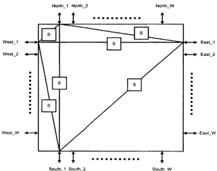
North_1 North_2 North_W
S S West-1 - - S East_1 West_2 0-- 4-> East_2 S * S . WestW *- 4-- East_W
South 1 South_2 SouthW
Figure 1-2: Switch block pins with different switch flexibility.
In switch blocks, the number of possible connections between one pin to other pins is called the flexibility of the pin. For example, in Figure 1-2, the switch flexibility of SouthW is 1, the flexibility of West_1 and South_1 is 2, the flexibility of North_1 is 3, and the flexibility of East_1 is 4. The pins that are not connected to anywhere have a flexibility of 0. Switch flexibility of 3 or 4 is suggested to be very optimum if all pins have the same flexibility [6]. It is shown that for 3-D FPGAs, switch flexibility of 5 provides optimum routability [7].
Many methods are proposed to improve the power consumption in switch blocks.
[5] analyzes different combinations of dual-threshold CMOS, sleep-transistors, body-source forward biasing, and low-swing technique to improve the power consumption in switch blocks. [8] utilizes a low-swing technique with a new way of clustering PLBs to improve the power and shows power improvement by an order of magnitude.
[9]
analyzes the optimum combination of tri-state buffers and pass-transistors to improve the power by 15%-20%.
opti-mized for best area and routabiliy. Many FPGAs utilize long wires that bypass a few switch blocks and connect distant switch blocks [11]. The number of long wires and their type (bypassing 1 switch block or more) is another parameter to optimize.
The performance of an FPGA also depends on the width of interconnect wires. Wider wires have smaller electrical and thermal resistance. Thermal resistance is particularly important in 3-D circuits. On the other hand, wider wires have larger self and coupling capacitance which increase both the delay and the power consumption. In addition to the width of interconnect wires, the size and type of each switch impact the performance. Switch blocks can be designed with pass-transistors, transmission gates, multiplexers, or tri-state buffers [11]. If each pin of a switch block can be connected to all other sides of the switch block, it is called a universal switch block.
[10] proposes a new architecture for universal switch blocks with switch flexibility of 3 that allows multi-pin net routing.
1.2
Overview of 3-D Integrated Circuits
As mentioned before, the delay of interconnect is one of the important factors which limits the performance of integrated circuits. One way to improve the performance of interconnect is to use 3-D integration of transistors.
Smaller wire length in 3-D corresponds to smaller capacitance on interconnect, and as a result, 3-D circuits are faster. It is shown that 31% to 56% speed improvement can be achieved with 3-D integration [12]. The speed improvement can be traded off for power saving by lowering Vdd. The power of 3-D circuits is reduced both because of reduced Vdd and reduced capacitance.
In this thesis, the 3-D layers of transistors are referred to as "active layers". In other publications, the layers are also called "device layer" [13], "tier" [14], and "stra-tum" [15]. There are many possible methods for 3-D integration of active layers. In Vertical Multi-Chip Module (MCM-V), dies are fabricated separately and bonded to a vertical Printed Circuit Board (PCB) [16] [17]. MCM-V connects the dies from their periphery to PCB and the connection has larger delay relative to on-chip connections.
Two other 3-D fabrication methods are ultra-thin chip stacking [18] [19]and multi-layer thin-film packaging [23]. In these methods, dies are thinned and bonded. Then the inter-layer connections are made through the periphery of the dies. These meth-ods offer better performance than MCM-V, but the delay of inter-layer connection is still large. Another method is flip-chip bonding [23] which is similar to flip-chip bonding to PCB.
Another method for 3-D fabrication is epitaxial 3-D integration. In this method silicon seeds are used to grow more transistors on the top of the current transistors [21]. Another similar method uses solid-phase re-crystallization where amorphous silicon is deposited on the die and laser is used for crystallization. This method is used to fabricate high-density memories [22].
The method that is considered in this thesis is wafer bonding. During the design of each active layer, 3-D wires are connected through 3-D inter-layer vias. During the fabrication, first different dies are fabricated with conventional methods. Then, they are bonded and 3-D connections are made by etching. While this method allows high density of inter-layer connections, the delay and area overhead of inter-layer Vias are larger than on-chip Vias.
One advantage of wafer bonding is the possibility of integrating different tech-nologies in one product. Different layers can use techtech-nologies for low-power SRAM or high-speed RF. Optimum physical partitioning is also a function of type of each layer. Another advantage of 3-D integration of dies is 3-D isolation. Since substrate noise in mixed-signal systems imposes many challenges and standard isolation techniques are less effective as frequency increases, 3-D integration of dies is utilized to provide substrate isolation between different circuit blocks [24].
3-D integrated circuits have their own challenges as well. In the fabrication phase,
the main challenge is efficient bonding of dies in 3-D (with lowest possible cost of via). In the design phase, the heat transfer is the main problem [25]. Dies at the middle of a 3-D structure encounter a large thermal resistance to the ambient, which increases the temperature of the die. One design method to reduce the temperature of the middle layers is to move the low-power circuits to the middle layer and high-power
circuits closer to the heat-sink. Another method is the usage of enough inter-layer via to transfer heat to adjacent layers. Because of the temperature problem at the center of 3-D structures and the cost of vias, increasing the number of 3-D layers does not always improve the power consumption or speed. In general, each system has an optimum number of device layers which may differ from other systems [261.
In addition to the above challenges, some other possible problems are reported for 3-D integration. One problem is the parasitic coupling between layers [27], and another is reliability of 3-D ICs (which includes electro-migration in 3-D structure and reliability of 3-D bonding) [28].
Chapter 2
Analysis of 3-D FPGAs
In this chapter, the delay and power improvement in 3-D FPGAs relative to 2-D FPGAs will be analyzed. First, Section 2.1 reviews the methodology to program
the 3-D FPGA. The performance of a 3-D FPGA depends on physical partitioning,
which determines how the circuit is split among several active layers. In Section 2.2, several physical partitioning options will be described, and one architecture will
be selected for further analysis. In Section 2.3, the block diagram of the FPGA chip will be described in detail. In Section 2.4, the wire length of the interconnect will be measured both for the case of a 2-D FPGA and a 3-D FPGA. Since one of the advantages of 3-D FPGAs is smaller interconnect delay [29], in Section 2.5, the delay improvement of 3-D FPGAs will be analyzed. Another advantage of 3-D is
improvement in power consumption. In Section 2.6, the power saving in 3-D FPGAs
will be analyzed.
2.1
Programming an FPGA chip
Before designing an FPGA chip, the flow to program the FPGA chip should be evaluated carefully. T-VPack and VPR can be used for placement and routing of benchmarks on the FPGA [30]. T-VPack is a CAD tool that maps logic blocks to PLBs. If several PLBs are clustered in a CLB, T-VPack can also map logic blocks to CLBs. The output of T-VPack can be sent to VPR. VPR is a placement and routing
tool for FPGAs which is developed at the University of Toronto for research purposes. In this research, the following method is used to program the FPGA. First, a given HDL code is synthesized with commercial synthesis tools. A program will be developed to convert the synthesized code to BLIF format. Then, T-VPack is used to map the design in BLIF format to PLBs or CLBs. Then, a customized placement and routing tool will be used for placement and routing. The tool will also generate the bit-stream to program the FPGA. The tool will be referred to as Customized Placement and Routing Tool (CPRT) in the rest of this thesis and is developed by Dr. Young-Su Kwon in our research group. Knowing how to program the chip and the requirement of the CPRT, the FPGA chip can be designed properly.
2.2
Possible 3-D Architectures
In order to determine a proper 3-D architecture, it will be shown how 3-D integration can improve the performance of the system. The delay of interconnect is one of the important factors which limits the performance of FPGA ICs and interconnect delay is more significant in each new technology generation of ICs. The delay of a wire is mainly due to its capacitance. Using lumped model for wires, their delay can be calculated by:
At = AV*CL (2.1)
where CL is the capacitance of the wire and I is the output current of the driver. At is the time required to result in Av voltage change.
To generalize the calculation for both short channel and long channel transistors, the a-model can be used [31] [32]. In this model, the current of a transistor can be calculated by:
I = 3(VGS - Vth) (2.2)
where / and a are constants that depend on the technology. a has a value of 2 for long channel transistors and approaches 1 for short channel transistors. In practice, the value is somewhere between 1 and 2. VGS is the gate-to-source voltage and Vth is
the threshold voltage of the transistor.
Assuming a constant output current for the driver and using the a-model, the delay of a wire can be calculated as:
Zo -CL
At = A CL(2.3)
Z (VGS - Vth)(2 In typical digital circuits, VGS is equal to Vdd.
In 3-D fabrication, circuit blocks can be placed closer to each other. Hence, the maximum wire length reduces. Smaller wire length corresponds to smaller capacitance on interconnect, and as a result 3-D, circuits are faster. The speed improvement can be traded off for power savings by lowering Vdd. The following formula shows the power consumption on interconnect:
P=a CL f _V (2.4)
where a is the activity factor, CL is the equivalent load capacitance,
f
is the operating frequency, and Vdd is the supply voltage.According to Equation 2.4, the power of 3-D circuits reduces both because of reduced Vdd and reduced capacitance, CL.
To take most advantage of 3-D circuits, it should be investigated how the FPGA should be physically partitioned in different active layers. Proper physical partitioning has a great impact on the performance improvement of the system. For example, in image-sensors, one layer is devoted to the sensors and another to corresponding ADCs to increase the density of sensors on the top layer [34]. As a result, while the density of sensors on top layer is increased, there is a short distance to ADCs which keeps the parasitic capacitances low.
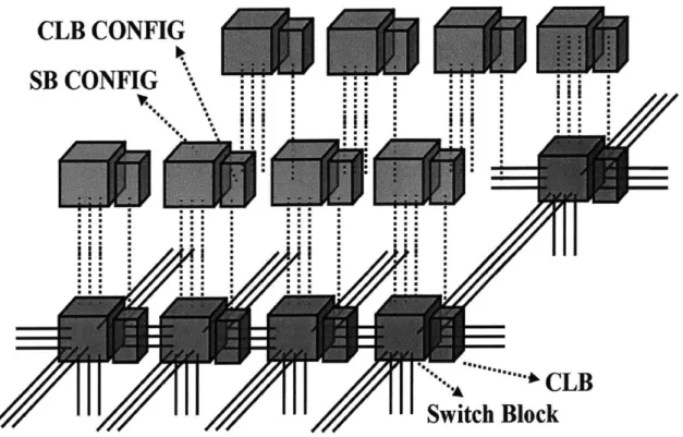
Figure 2-1 shows one possible architecture for a 3-D FPGA. In this architecture, different active layers have the same structure; all layers have Configurable Logic Blocks (CLB), Switch Blocks (SB), and the configuration blocks. The connection between blocks is similar in all active layers. The advantage of this architecture is that logic blocks that were far away in a 2-D FPGA are now much closer at the upper
SI CLB CONFIG CLB Switch Block B CONFIG
0 - -,
III
IIIIII
Figure 2-1: General Block Diagram of a 3-D FPGA.
or lower layers. For example, if a 2-D FPGA with 40 x 40 CLBs is integrated in 4 active layers, the size of the FPGA in each layer is 20 x 20 CLB. The distance between two CLBs at the opposite corners of the 2-D FPGA is 39 + 39 = 78. However, in the
3-D FPGA, the distance between two CLBs at the opposite corners is 19 + 19 + 3 =
41. This example shows how the distance between CLBs reduces in the architecture of Figure 2-1. In addition, there are more degrees of freedom during the routing since the third dimension can be also employed.
In FPGAs, the configuration blocks provide constant voltages to the functional circuit. These constant voltages are not subject to any timing requirement and can be placed anywhere. One possible architecture is based on placing configuration cells on a different layer as shown in Figure 2-2. In this architecture, one active layer is devoted to configuration cells and another active layer is devoted to functional circuits (programmable logic and switches). This approach can be generalized to more layers
by alternating between configuration layer and functional layer.
ze-'e
11
a.
-
CLB
Switch Block
Figure 2-2: A 3-D FPGA Architecture with one Layer.
Configuration Layer and one Active
From the experimental layouts, it was found that the size of configuration blocks is close to their corresponding functional block (switch block or CLB). As a result, if the configuration blocks could be moved to another layer with no overhead, the area of each tile would reduce by a factor of two and the length of interconnect would reduce by square root of two. The delay and power dissipation of interconnect would
also reduce because of the shorter capacitance on interconnect.
However, current technology requires a large inter-layer via for 3-D connection to other active layers. The size of the via depends on the accuracy of aligning two dies during the bonding process. A tile may have a few thousand configuration cells. If all configuration cells are placed in another layer, the area overhead of 3-D connections will be too high. Depending on the technology, the area overhead of 3-D connection may even exceed the original area used by configuration cells since the size of a latch scales with fabrication technology of each die and the size of an inter-layer via scales
CLB CONFIG
SB CONFIG
-
* 3Im* III
with the accuracy of the die alignment.
Split Switch bloc
I
I
SB CONFIG Switch Block CLB CLB CONFIGFigure 2-3: A 3-D FPGA Architecture with Switch Block Split in two Active Layers.
Figure 2-3 shows another possible architecture for physical partitioning. In this architecture, the switch block is split in two or more active layers. Since each CLB has a limited number of connections to its switch block, the number of required inter-layer vias is small. Therefore, the area overhead of this architecture (due to inter-inter-layer via) is reasonable. This approach requires more research on placement and routing of split switches to determine their routability. Based on their routability, it should be decided how to split the switch block to improve delay or power consumption.
In summary, placing configuration blocks in a separate layer (Figure 2-2) is not efficient because of area overhead. Both splitting the switch block in several layers (Figure 2-3) and integrating regular tiles in several layers (Figure 2-1) are expected to show delay and power improvement. The architecture of Figure 2-1 is used for delay and power analysis of 3-D FPGAs.
2.3
Block Diagram
In this section, the block diagram of the FPGA will be described. The circuit will be used in the following sections to analyze delay and power improvement in 3-D
architecture comparing to 2-D.
ConfI Conf 2 "-- Conf_16 F1 F2 Out F3 FF F4
---Figure 2-4: Programmable Logic Block (PLB).
The basic Programmable Logic Block (PLB) is shown in (Figure 2-4). A PLB consists of a 16-input MUX that functions as a lookup table, a Flip-Flop (FF), and a Multiplexer (MUX) at the output. The inputs of the PLB are the select signals of the 16-input MUX (lookup table). The second MUX can be used to select between the output of the LUT and the output of the FF. The configuration signals are provided
by configuration cells. The values of configuration bits define the functionality of the
PLB.
The design of the configuration cell is similar to typical SRAM cells with a few differences. One difference is that the output of the configuration cell is always connected to the output pin. This means that the output is constantly read. In addition, the cell is written from one side as opposed to typical SRAM cells that are written from both sides. When the FPGA is powered up, random values on configuration bits may cause two blocks to drive the same node to opposite logic values. The result is a large destructive current that may burn out the chip. A reset signal makes sure that during the power-up, all the tri-state buffers are turned off.
Figure 2-5: The Block Diagram of Configurable Logic Block.
Clustering several PLBs improves the performance of the FPGA since many PLBs are connected to the adjacent PLBs. Clustering PLBs also reduces the switch-block delay and area overhead. A cluster of four PLBs is shown in Figure 2-5 and is called a Configurable Logic Block (CLB). The CLB has 16 inputs and each one of them can be connected to any inputs of each PLB. In addition, the output of any PLB can be connected to any input of the other PLBs. InputMUX in Figure 2-5 chooses between the 16 inputs to the CLB and the 4 outputs of PLBs. Figure 2-6 shows the implementation of Input-MUX.
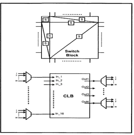
Figure 2-7 shows the block diagram of a 2-D Switch Block (SB). The number of connections to each side of the switch block is called the width (W) of the switch block. The pins on each side are numbered from 1 to W and can be either input or output. In this experiment, a disjoint switch block is used which is a simple switch block and is well supported by our CAD flow for programming the chip. In disjoint switches, pin n on one side is connected to pin n on all other sides through a switch cell (where n can be any number from 1 to W). In Figure 2-7, each switch cell is represented with block S and can be either a transmission-gate or a tri-state buffer. Two back-to-back tri-state buffers can be used as a bi-directional switch cell. All possible connections for pin number 1 are shown in the figure. The size of the switch
OutI-Out4 In I-In 16
Out I-Out4 Inl-In16 I
input MUX nputMUX PLB Outl
Input MUX inpnputMUX 1n2 1n3 PLB Out2 1n4 1n163
Input MUX InputMUX Out4
2 SRAM Outl Out2 Out3 Out4 In1 In2 In16 4 SRA
Figure 2-6: The Block Diagram of Input-MUX.
block depends on the number of switch cells in the switch block. A 2-D disjoint switch has 6W switch cells. The flexibility of this switch is 3 since each pin is connected to
3 other pins.
Table 2.1: Comparing 2-D and 3-D switch blocks.
Description Value
Number of pins in 2-D switch blocks 4W
Number of pins in 3-D switch blocks 6W
Ratio of pins in 3-D and 2-D switch blocks 6/4
Number of switch cells in 2-D switch block 6W
Number of switch cells in 3-D switch block 15W
Ratio of switch cells in 3-D and 2-D switch block 15/6
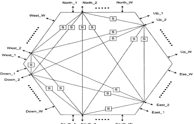
Figure 2-8 shows the block diagram of a 3-D switch block. Similar to 2-D switch block, the switch width is named W. North, South, East, and West pins make con-nections to tiles in the same active layer. Up and Down pins connect to tiles in the upper or lower layer. As summarized in Table 2.1, the 3-D switch has 6/4 times more pins available for routing and is a disjoint switch with a switch flexibility of 5. The total number of switch cells in this switch block is 15W. Note that the 3-D switch has 15/6 times more switches in the switch block.
Figure 2-9 shows the block diagram of a tile. A tile consists of a CLB, a switch block, MUXes and de-multiplexers that connect the switch block to the CLB, and all
North_1 North_2 North_W West_1 4-
i
' East_1 West_2 4-0 East_2 S S0 WestW 4 East_WSouth_1 South_2 SouthW
Figure 2-7: The Block Diagram of 2-D Switch Block.
configuration cells for these blocks. The configuration cells are not shown in the figure for simplicity. The pins of the switch blocks are connected to the pins of the tile. The inputs of each MUX are connected to one side of the switch block. Each input of the CLB is connected to a MUX that can select from W pins on the switch block. The outputs of the CLB are connected to de-multiplexers that have W outputs. The outputs of each de-multiplexer are connected to one side of the switch block.
Any of W inputs of MUXes and W outputs of the de-multiplexer can be connected to any pin on the switch block without affecting our analysis in the next sections.
The architecture of the PLB and the CLB is compatible with the available CAD tools for programming the FPGA. The CAD tool is developed by Dr. Young-Su Kwon for programming 3-D FPGA. The connection of the CLB to switch block and the architecture of the switch block are not constrained by the tool flow.
2.4
Wire Length Estimation
In this section, the wire length of interconnect will be evaluated. It will be shown that some 3-D properties of a tile tend to make 3-D tiles larger than 2-D and some
North_1 North_2 North_W WestW S Up_2 S 0 S S S* West 2 U pW West_1 S Down_1 EasW Down_2 *,S S East_2 Down W East_1
South_1 South_2 South_W
Figure 2-8: The Block Diagram of 3-D Switch Block.
other properties tend to make 3-D tiles smaller than 2-D tiles. At the end, it will be shown that 3-D tiles are slightly smaller than 2-D tiles.
The length of interconnect depends on the size of the tile and the size of a tile is mainly determined by the size of the switch block. On the other hand, the size of a switch block is a function of the channel width (since it determines the number of switch cells). As a result, to determine the length of interconnect wires, the channel width of interconnect should be determined.
Once the length of interconnect is determined, using the resistance and capacitance of a unit length wire, an RC model of interconnect can be obtained in the form of an L, T, or 7r model. The RC model will be used in Section 2.5 to evaluate the delay of interconnect. Since the performance of an FPGA depends on the delay on interconnect, this analysis helps to evaluate the performance of an FPGA.
To evaluate the effect of the channel width on the length of interconnect, the layout of 2-D tiles and 3-D tiles are prepared with different channel widths. Figure
SS S S S Switch Block I 2 Out1 Out2 CLB Out3 Out4 2 2 -in_16
Figure 2-9: The Block Diagram of a Tile.
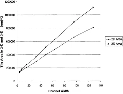
2-10 shows the area of different layouts with different channel widths in 2-D and 3-D. The area in 3-D is larger because of two reasons. First, inter-layer vias (the connection to the top or bottom active layer) require dedicated area, and nothing can be placed above or below them. Secondly, the number of switch cells in a switch block is much larger in 3-D as described before. As a result 3-D tiles tend to be larger than 2-D tiles.
Figure 2-11 shows the area penalty in a 3-D tile due to inter-layer via overhead and a larger number of 3-D switches. The area of the tiles is obtained from the layout and it includes the CLB, the switch block, the configuration bits for all cells, and the area of the inter-layer via. While the initial concern was the area overhead due to inter-layer via, the area overhead of 3-D switch blocks is shown to be much larger. The area overhead of a 3-D switch block approaches 33% for a channel width of 128. There are a few important factors that are not taken into account in the above comparison. The switch blocks in 3-D have many more pins connected to them (6W)
1200000-1000000 E 800000 A 600000 400000 200000 0 2D Area -a-3D Area 0 20 40 60 80 100 120 140 Channel Width
Figure 2-10: The Area of Tile Vs. the Channel Width of Interconnect.
compared to a 2-D switch block (4W). In addition, a larger number of switch cells in a 3-D switch block (15W) compared to a 2-D switch block (6W) results in improved routability in 3-D. Some circuits that are not routable in 2-D at all may be easily routable in the 3-D version if the channel width is the same. To compare the 2-D structure to 3-D properly, both architectures should have similar routability.
Two basic metrics can be used to represent the routability:
* total number of wires connected to a switch block (since there are more wires
available during the routing)
* number of switch cells in a switch block (since there is more flexibility of con-necting different wires and avoid congestion)
Choosing either of them suggests that the channel width of 3-D should be reduced to match routability. In the first case, the channel width should be reduced by a factor of 4/6 and in the second case by a factor of 6/15. The second metric reduces the area of a 3-D tile significantly and will result in more delay and power improvement. In order to avoid overestimation of 3-D benefits, the first metric (having equal number of wires connected to switch block) is chosen for the rest of analysis.
35.0 30.0 C 25.0-£ 20.0 2+Via Overhead 1. -- Swtch Penafty C: 10.0 0 M 5.0 0.01 0 20 40 60 80 100 120 140 Channel Width
Figure 2-11: The Area Penalty in 3-D Tiles Comparing to 2-D Tiles due to Inter-Layer Via and 3-D Switch Block as a Function of the Channel Width of Interconnect.
Figure 2-12 shows the length of interconnect as a function of total number of wires connected to a switch block. To obtain the channel width corresponding to each point on the graph, the total number of wires should be divided by 4 in the case of 2-D and
by 6 in the case of 3-D. The graph shows that the area of 3-D tile is almost the same
as 2-D tile with the chosen routability metric. While the larger number of switch cells in the 3-D switch block and the area overhead of inter-layer vias tend to increase the size of 3-D tiles, the smaller channel width in 3-D switch blocks tends to decrease the size of 3-D tiles. In the channel width of our interest (W=4 to W=128), the two factors almost cancelled out. In addition to comparing the interconnect length in 2-D and 3-D, the graph will be also used to determine the length of interconnect for delay calculation.
Based on placement and routing of several benchmarks, it was found that for a
2-D FPGA with 40x40 tiles, the channel width of 96 provides proper routability (which
corresponds to the total number of wires equal to 384). The equivalent 3-D channel width with the chosen routability metric is 64. The corresponding interconnect length in 3-D is 792pm and in 2-D is 815t.
1000 900 800 700 cc 600 a A500 -.- ie Length2-D) C -a--Tile Length 3-D 0 4 4 00 00 100 0 0 100 200 300 400 500 600 700
Total Number of Wires Connected to a Switch Block
Figure 2-12: The Length of Interconnect Vs. the total number of wires connected to the switch block.
The wire length estimate in this section is based on Lincoln Lab 0.18pm process with FDSOI (Fully Depleted Silicon On Insulator). The technology utilizes 3 metal layers. In the case of an FPGA, whose performance is limited by the interconnect delay, more metal layers improves the performance of interconnect significantly. To
avoid wiring congestion during the layout, wiring channels are assigned in the layout between the rows of standard cells (with no circuit underneath the wiring channel). The wire channels increase the area of the tile. The size of the dedicated wire channels in the layout is the same in 2-D and 3-D layout. The area estimate is obtained by automatic layout generation (ASIC flow).
2.5
Delay Analysis
Once the HDL description of a digital system is ready, it will be converted to an equivalent circuit that has the same functionality. This process is called synthesis. Different synthesis tools may synthesize the same HDL code differently. While the results have the same functionality, their performance, power consumption and area
may differ. In addition, the use of different options during the synthesis may force the program to optimize the circuit for lower area, better performance, or less power consumption. As a result, the HDL synthesis process affects the performance of the implemented code on an FPGA chip.
After an HDL code is synthesized, it will be implemented on an FPGA in two steps. In the first step, it will be decided which programmable logic blocks should be used to implement each block of the synthesized code. This process is called placement. In the second step, it will be decided how the programmable interconnect can be used to connect different blocks according to their connectivity in the synthesized circuit. This process is called routing. There are many placement and routing algorithms with different advantages. The performance of a circuit on an FPGA depends on the efficiency of the placement and routing tool.
In addition to the above factors, the performance of a circuit on an FPGA depends on the type of the circuit (functionality), the chosen architecture, the complexity of the system and many other factors. As a result, different implemented circuits on an FPGA may operate at a different speed. This means that it is not possible to determine the speed of an FPGA without knowing the implemented circuit.
In this section, the performance of FPGAs will be analyzed by evaluating the delay improvement in 3-D FPGAs comparing to 2-D. The emphasis of the analysis is on comparing 2-D and 3-D FPGAs regardless of synthesis, placement, and routing algorithms. The FPGA can be viewed as many CLBs that are connected to each other using the programmable interconnect. While it is not known prior to placement and routing which connections are made, the delay of each possible connection can be determined. To analyze the delay of FPGAs, the delay of all possible point-to-point connections (from one CLB to another CLB) is determined. A histogram of point-to-point delays shows the number of possible connections in an FPGA with different delays. Then, by comparing the histograms in 2-D and 3-D, their delay can be compared.
The delay in point-to-point connection is due to:
_ _ _ Path2 S
* Tile to tile
Switch . interconnect Switch
Block Block
PLCLB
W ---- Path1
CLB CLB
Tile 1 Tile 2
Figure 2-13: Different Segments of a Connection from a FF in One Tile to Another FF in an Adjacent Tile.
block (Pathi in Figure 2-13)
" The delay of switch blocks and interconnect from the source tile to the
desti-nation tile (Path2 in Figure 2-13).
" The delay of a signal from a switch block through all MUXs and the PLB to
the input of a FF (Path3 in Figure 2-13)
Spice simulation is used to measure the delay from a switch block to a FF and from a FF to a switch block (the first and last items mentioned above). To calculate the delay of interconnect and switch blocks, the equivalent RC model of buffers and switches is obtained from Spice simulation. The equivalent RC model of a unit length wire is obtained from Lincoln Lab documentation; then, the equivalent RC model for interconnect is obtained by scaling the RC model of wires according to the length of the interconnect. Table 2.2 shows the delay obtained from Spice simulation and the
equivalent capacitance and resistance of basic blocks.
Table 2.2: Summary of values used for delay estimation
Description Value
Length of interconnect in a 2-D FPGA 815pm
from a tile to an adjacent tile (for channel width of 96)
Length of interconnect in a 3-D FPGA 792[m
from a tile to an adjacent tile (for channel width of 64)
Wire capacitance 64 fF/mm
Wire resistance 400 (/mm
Delay from FF to Switch block 0.201 ns
Delay from Switch Block to FF 2-D 1.002 ns
Delay from Switch Block to FF 3-D 0.942 ns
Input capacitance of tri-state buffer 8.8 fF
Output resistance of tri-state buffer 2.1 KQ
Output capacitance of tri-state buffer 14.2 fF
Inter-layer Via resistance 0.15 Q
Inter-layer Via capacitance 3.5 fF
Equivalent resistance of pass transistor 2.1KQ
Equivalent capacitance of pass transistors 14.2fF
Switch cells in switch block can be either transmission gates or tri-state buffers.
3-D delay improvement will be analyzed for both types of switch cells. Figure 2-14
shows the delay histogram of point-to-point connections in 2-D and 3-D FPGAs when transmission gates are used. The transmission gates include a PMOS and an NMOS in parallel to avoid Vth drop when logic value of 0 or 1 is transmitted (VON = Vdd). The
2-D FPGA has 15x15 tiles in one active layer. The 3-D FPGA has 15x5 tiles in three
active layers. So the total number of tiles and possible point-to-point connections is the same in both cases. The first graph on Figure 2-14 is the delay histogram of the
2-D FPGA, the second graph is the delay histogram of the 3-D FPGA, and the third
graph is the delay histogram of 2-D and 3-D on the top of each other.
The maximum delay is 21ns in the 2-D FPGA and is 9.8ns in the 3-D FPGA and shows 53% delay improvement in 3-D. The average delay is 5.1ns in 2-D and is 3.2ns in 3-D and shows 37% improvement in 3-D. In this analysis, it is assumed that the shortest path between any two points is available for routing and the signal is sent to only one final CLB (fanout of one). [35] uses a stochastic model to estimate the
2000-Delay histogram in 2-D 1000-0 5 10 15 20 2 Delay of point-to-point pa [ns] 3000 - 2000-Delay histogram in 3-D 1000
i
0 510 15 20 2Delay of point-to-point path fns]
Comparng delay histogram of
2-D a.d 3-D
1000-
iliki~L
1
1IIIIi
0 5 10 15
Delay Of Pointto-point path [ns] 20
5
5
25
Figure 2-14: The Delay Histogram of Point-to-Point Connections and the 3-D FPGA with Transmission Gates as a Switch Cell.
in the 2-D FPGA
delay improvement in 3-D FPGA and shows 54% delay improvement in the longest path on 3-D FPGA (with 3 active layers and no buffers).
Figure 2-15 shows possible options for a switch cell. If tri-state buffers are used instead of transmission gates in switch cells, the delay will improve both in the 2-D
FPGA and in the 3-D FPGA. The delay histogram of 2-D and 3-D FPGAs when the
signals are buffered is shown in Figure 2-16. The 2-D FPGA has 15x15 tiles in one active layer and the 3-D FPGA has 15x5 tiles in three active layers. The maximum delay is 6.lns in 2-D and is 4.3ns in 3-D and shows 29% improvement in 3-D. The average delay is 2.9ns in 2-D and is 2.3ns in 3-D and shows 20.6% improvement in
3-D. The stochastic model used in [35] shows 42% delay improvement in the longest
Inout1 f
Pass Tra
E Eni
En
I InOut1 InOut2 InOut1 InOut2
Lnut2
~nb En2
nsistor Transmission Gate Tri-state Buffers
Figure 2-15: Possible Options for a Switch Cell.
It should be noted that the delay of a combinational logic implemented on FPGAs may be much larger than the maximum delay of point-to-point path because of two reasons. First, the routing may not be over the shortest path because of congestion. Secondly, a combinational path may go through many CLBs before it is terminated to a FF. In other words, several point-to-point connections together may constitute a single combinational path. However, the 3-D delay improvement shown here cor-responds to the delay improvement in the 3-D FPGA after a circuit is placed and routed.
2.6
Power analysis
Power analysis in this section is carried on for an FPGA whose switch cells are tri-state buffers. The power improvement in the 3-D FPGA is due to two factors:
* Tiles are placed closer to each other which causes the switching capacitance of interconnect to be smaller. Lower capacitance corresponds to lower power consumption.
" Since the delay is improved, the FPGA can operate at a lower supply voltage to
have the same performance. Lower supply voltage lowers the power consump-tion of the FPGA in 3-D.
To analyze the power improvement, first it will be analyzed how the delay of a digital circuit changes as the supply voltage varies. Then, the energy consumption
3DDOII I
2-D Histogram
1000-0. I hiiiI.
1 2 3 4 5 6 7
Delay of point4o-pon path IrnsJ
3000
2DOO -3-D listogram
1000-0 _ [nsj11111M II _
1 2 3 4 5 6 7
Delay Of point-point path [s
2I00I Comparing 2-Dand 3-D Histogram
1000 F
OL
3 4 5
Delay of pointo-point path [ns]
6 7
Figure 2-16: The Delay Histogram of Point-to-Point Connections in the 2-D FPGA and the 3-D FPGA with Tri-State Buffers as a Switch Cell.
of different blocks will be measured. Finally, a histogram of energy dissipation in all point-to-point connections will be generated for 2-D and 3-D FPGAs.
Equation 2.3 shows the time required to change the output voltage of a circuit
by Av. If Av is half of the supply voltage and VGS equals the supply voltage, At corresponds to the delay of the circuit (as shown in Equation 2.5). In this analysis, the rise-time and fall-time are assumed to be very small. Using Equation 2.5, the delay of a circuit can be calculated as supply voltage changes:
delay = 2V
1.8 1.6 *1.4 1.2 -+- Measured Delay 0-- Calculated Delay 00.6 -_ 0. o 0.4 0.2 0 0 0.2 04 0,6 0.8 1 1.2 1.4 16 1.8 2 Vdd [v]
Figure 2-17: The Delay of Tri-State Buffer vs. Vdd.
Since the delay of FPGAs is dominated by the delay of interconnect and intercon-nect is driven by tri-state buffers, it is assumed that the delay of FPGA chips is scaled with supply voltage the same way as tri-state buffer. Figure 2-17 shows the delay of tri-state buffer when the supply voltage is scaled. It shows both the simulated values and calculated values (based on Equation 2.5). The value of a is 1.6 and is calculated from simulation.
It is expected that by keeping the activity factor and load capacitance constant, the energy dissipation per cycle is proportional to V. Figure 2-18 shows how well the measured energy dissipation of a MUX follows the expected values. In this simulation the rise-time and fall-time are kept constant and a linear capacitance is added to the load to suppress non-linear output capacitance of the MUX.
Figure 2-19 shows the energy dissipation of different parts of a tile. In this graph, the energy dissipation of input decoder corresponds to energy dissipation in all input MUXes in a tile and in CLB plus the energy dissipation in LUT. The energy dissi-pation of the output decoder corresponds to the energy dissidissi-pation of a FF and the output MUX in a tile. The energy dissipation of an internal loop corresponds to the energy dissipation of a circuit from the output of the FF in one PLB to the input
9.OOE-13 8.OOE-13 7.OOE-13 6.OOE-13 5.OOE-13 -+- Simlated -.- Calcuiated 3.OOE-13 6 2.00E-133 1.OOE-13 O.OOE+00 0 0.2 0.4 0.6 0.8 1 1.2 1.4 1.6 1.8 2 Vdd [v]
Figure 2-18: Energy Consumption of MUX vs. Vdd.
of the FF in another PLB, all in the same CLB. Energy dissipation of interconnect corresponds to interconnect between two adjacent tiles.
Figure 2-19 shows that if a tile is connected to an adjacent tile, the energy dis-sipation is not dominated by interconnect. However, if the destination tile is more than 3 tiles away, the energy dissipation due to interconnect is more than 50% of the total energy. It should be noted that the energy dissipated on the clock tree and the leakage power are not taken into account in this analysis.
The following example illustrates the power consumption of the FPGA. If the
FPGA is operating at 100MHz and contains 10,000 nets that are connected from a
tile to an adjacent tile, the power consumption of the FPGA is 0.3W. It is assumed that the supply voltage is at 1.8V and the activity factor of all signals is 0.25. If the supply voltage is lowered to 0.8V and the operating frequency is kept at 100MHz, the power consumption of the FPGA is 0.05W.
Finally, the power improvement in the 3-D FPGA can be analyzed by plotting a histogram of energy dissipation of all possible point-to-point connections (per cycle). Figure 2-20 shows the histogram when both the 2-D FPGA and the 3-D FPGA are running at the same supply voltage, 1.8V. There is 22% energy improvement in the
8.00E-13
7.00E-13
6.00E-13
M 5.00E-13 _+- Input decoder 2D
/2- Input decoder 3D 4E1Output decoder C. -+-Internal loop C+-- FF o- Interconnect U 3.OOE-13 / 2.00E-13 1.00E-13 O.OOE.00 0 0.2 0.4 0.6 0.8 1 1.2 1.4 1.6 1.8 2 Vdd [V]
Figure 2-19: Energy Consumption of Different Parts of a Tile Vs. Vdd.
longest path and 17% energy improvement in average. Appendix A explains why the
3-D histogram does not have a smooth bell shape (similar to the smooth bell-shape
in 2-D).
According to earlier analysis, 20% to 29% delay improvement can be achieved in
3-D comparing to 2-D. According to Figure 2-17, the power supply can be reduced
from 1.8V to 1.6V to trade-off the delay improvement with more power improvement in 3-D. Figure 2-21 shows the energy dissipation histogram in 2-D and 3-D FPGAs. The maximum energy dissipation is 14pJ/cycle in 2-D and 8.6pJ/cycle 3-D, which corresponds to 39% energy improvement in 3-D. The average energy dissipation is 6.lpJ/cycle in 2-D and 3.9pJ/cycle in 3-D. It corresponds to 35% energy improvement in 3-D. [35] shows 35%-55% power improvement in 3D FPGA.
In summary, the 3-D FPGA can be used to provide 20%-29% improvement in delay and 17%-22% improvement in power. If the delay improvement is traded off with more power improvement, 35%-39% power improvement is expected.
co ts 3000 S2000 -2-0 Histogram -2-D Histogram 1000-2 0
.iiiIIII
iiE..~
.
05 10 15Energy dissipation per cycle [pJ]
O 3000 o 2000-Cp3-D Histogram 0- 1000-E 0LAIIII z 0 5 10 15
Energy dissipation per cycle [pJ]
a-0 Compating 2-D and t a 3-a_
1000-E
0
z 0 5 10 15Energy disipton per cycle [pJ]
Figure 2-20: Histogram of Energy Consumption of All Point-to-Point Connections without Scaling Supply Voltage in 3-D.
4000 S
3000-0
a- 2-D Histogram
0 5Eey dsptinprycep]10 15
0 5~Energy dissipation per cycle [10 1
4000 cc 30-0 .0 E Z 0 5 10 15
Energy dissipation per cycle [pJJ S 4000 cc : HistogramoAPin-t C r a p g E.000
II-1
E 0-0
5105Energy dissipation per cycle [pJ]
Figure 2-21: Histogram of Energy Consumption of All Point-to-Point Connections after Scaling the Supply Voltage in 3-D.
Chapter 3
Fabricated Chip
A chip is fabricated in 3-D technology to measure the delay and power improvements in a 3-D FPGA. This chapter describes different steps of designing the chip.
3.1
Hardware Design of the Fabricated Chip
The first important block to be designed in this project is the CLB. The design of the CLB should be compatible with the placement and routing tool. The CLB is
designed with additional circuits to implement adders, multiplexers and shift registers
more efficiently. First, the CLB was designed and tested on its own. Then, the functionality and interaction of several CLBs was simulated. In this test, an HDL code was synthesized and mapped to LUTs/CLBs. To simplify the test, the pins of CLBs were connected directly (without going through switch blocks). The simulation improved the compatibility between the placement and routing tool, and hardware from early stages of development. The next goal is to create the full Verilog model of the FPGA chip. Designing FPGA chips always require careful tradeoff between the following parameters:
" Architecture of a Switch Block
* Type of switch cells (transmission gates vs. tristate buffers) * Size of transistors in the switch
. Number of long wires and short wires. * Area of a Switch block
* The connection of CLB to the switch block
To provide a proper flow for designing an FPGA, a program is developed to gener-ate the description of the FPGA automatically. The program reads in an architecture file and it generates a Verilog description of the FPGA based on the architecture file. The architecture file defines the following:
* The number of active layers
* The number of tiles in each row and column
" The type of interconnect (i.e. single, double, long, etc.) and the channel width
for each type (W)
" The architecture of the switch block and the type of switch cells
* The connectivity of the CLB to the switch block
When the architecture of a switch block is being defined, any combination of possible connections between different pins can be defined together with the type of switch cell for each connection. The placement and routing tool is fully compatible with the architecture file and reads in the same architecture file to program the FPGA. As a result, one can change the architecture of the FPGA and redesign it with little effort. The benefit of this approach is that the performance of different types of FPFAs can be easily evaluated. This flexibility is used in Section 2.4 to generate many FPGAs with different channel width and evaluate the area of tile as a function of channel width. Table 3.1 describes the parameters used in the architecture file for this chip.
One step in designing an FPGA chip is to design the required circuitry to program the configuration cells. If the configuration cells are implemented using FFs, they