• Aucun résultat trouvé

Versatile molecular silver ink platform for printed flexible electronics

N/A
N/A
Protected

Academic year: 2021

Partager "Versatile molecular silver ink platform for printed flexible electronics"

Copied!
13
0
0

Texte intégral

(1)

Publisher’s version / Version de l'éditeur:

ACS Applied Materials & Interfaces, 9, 20, pp. 17226-17237, 2017-05-03

READ THESE TERMS AND CONDITIONS CAREFULLY BEFORE USING THIS WEBSITE. https://nrc-publications.canada.ca/eng/copyright

Vous avez des questions? Nous pouvons vous aider. Pour communiquer directement avec un auteur, consultez la première page de la revue dans laquelle son article a été publié afin de trouver ses coordonnées. Si vous n’arrivez pas à les repérer, communiquez avec nous à PublicationsArchive-ArchivesPublications@nrc-cnrc.gc.ca.

Questions? Contact the NRC Publications Archive team at

PublicationsArchive-ArchivesPublications@nrc-cnrc.gc.ca. If you wish to email the authors directly, please see the first page of the publication for their contact information.

NRC Publications Archive

Archives des publications du CNRC

This publication could be one of several versions: author’s original, accepted manuscript or the publisher’s version. / La version de cette publication peut être l’une des suivantes : la version prépublication de l’auteur, la version acceptée du manuscrit ou la version de l’éditeur.

For the publisher’s version, please access the DOI link below./ Pour consulter la version de l’éditeur, utilisez le lien DOI ci-dessous.

https://doi.org/10.1021/acsami.7b02573

Access and use of this website and the material on it are subject to the Terms and Conditions set forth at

Versatile molecular silver ink platform for printed flexible electronics

Kell, Arnold J.; Paquet, Chantal; Mozenson, Olga; Djavani-tabrizi, Iden;

Deore, Bhavana; Liu, Xiangyang; Lopinski, Gregory P.; James, Robert;

Hettak, Khelifa; Shaker, Jafar; Momciu, Adrian; Ferrigno, Julie; Ferrand,

Olivier; Hu, Jian Xiong; Lafrenière, Sylvie; Malenfant, Patrick R. L.

https://publications-cnrc.canada.ca/fra/droits

L’accès à ce site Web et l’utilisation de son contenu sont assujettis aux conditions présentées dans le site LISEZ CES CONDITIONS ATTENTIVEMENT AVANT D’UTILISER CE SITE WEB.

NRC Publications Record / Notice d'Archives des publications de CNRC:

https://nrc-publications.canada.ca/eng/view/object/?id=e60de2ce-06b0-4ab9-8184-da3a4e3d7a78 https://publications-cnrc.canada.ca/fra/voir/objet/?id=e60de2ce-06b0-4ab9-8184-da3a4e3d7a78

(2)

Versatile Molecular Silver Ink Platform for Printed Flexible

Electronics

Arnold J. Kell,

*

,†

Chantal Paquet,

Olga Mozenson,

Iden Djavani-Tabrizi,

Bhavana Deore,

Xiangyang Liu,

Gregory P. Lopinski,

Robert James,

§

Khelifa Hettak,

§

Jafar Shaker,

§

Adrian Momciu,

§

Julie Ferrigno,

Olivier Ferrand,

Jian Xiong Hu,

Sylvie Lafrenière,

*

,∥

and Patrick R. L. Malenfant

*

,†

Security and Disruptive Technologies Portfolio and ‡

Measurement Science and Standards Portfolio, National Research Council Canada,100 Sussex Drive, Ottawa, ON K1A 0R6, Canada

§

Communications Research Centre Canada, RF Technologies, 3701 Carling Avenue, Ottawa, ON K2H 8S2, Canada

GGI International, 1455, 32e Avenue, Lachine, QC H8T 3J1, Canada

*

S Supporting Information

ABSTRACT: A silver molecular ink platform formulated for screen, inkjet, and aerosol jet printing is presented. A simple formulation comprising silver neodecanoate, ethyl cellulose, and solvent provides improved performance versus that of established inks, yet with improved economics. Thin, screen-printed traces with exceptional electrical (<10 mΩ/□/mil or 12 μΩ·cm) and mechanical properties are achieved following thermal or photonic sintering, the latter having never been

demonstrated for silver-salt-based inks. Low surface roughness, submicron thicknesses, and line widths as narrow as 41 μm outperform commercial ink benchmarks based on flakes or nanoparticles. These traces are mechanically robust to flexing and creasing (less than 10% change in resistance) and bind strongly to epoxy-based adhesives. Thin traces are remarkably conformal, enabling fully printed metal−insulator−metal band-pass filters. The versatility of the molecular ink platform enables an aerosol jet-compatible ink that yields conductive features on glass with 2× bulk resistivity and strong adhesion to various plastic substrates. An inkjet formulation is also used to print top source/drain contacts and demonstrate printed high-mobility thin film transistors (TFTs) based on semiconducting single-walled carbon nanotubes. TFTs with mobility values of ∼25 cm2V−1s−1and

current on/off ratios >104were obtained, performance similar to that of evaporated metal contacts in analogous devices. KEYWORDS: Printed flexible electronics, additive manufacturing, conductive molecular inks, metal organic decomposition (MOD), photosintering

1. INTRODUCTION

Printable electronics, an additive manufacturing technology,1 combines electronic materials with conventional printing processes to enable large-area, flexible, and/or low-cost manufacturing of membrane switches,2 thin film transistors (TFTs),3and sensors4as well as photovoltaics,5antennas,5and organic light-emitting diode (OLED)-based displays.4

Con-ductive inks make up one of the largest markets in printed electronics as they enable the fabrication of key elements such as electrodes, antennas, and bus bars for current collectors using gravure,3,6aerosol jet,7inkjet,3,4,8or screen printing.8−12

Each of these printing techniques has its attributes, but the screen printing of silver flake inks is the most mature technology and remains the most widely utilized technique currently used in the manufacture of conductive elements.12,13 These flake-based inks can produce traces with good electrical properties (sheet resistivity values of 10−15 mΩ/□/mil and volume resistivity values of 18−25 μΩ·cm) and typically have thicknesses of ∼4−15 μm, which is required to attain reliable mechanical properties and maximize electrical conductivity.12,13 The printed electronics industry is driven, in part, by a desire to

exploit additive manufacturing to reduce cost, and simply decreasing the silver content and the resulting trace thickness is an obvious means of achieving that goal. However, there are practical limitations in achieving high conductivity and mechanical robustness with flake-based inks because the traces require overlap of multiple layers of silver flakes and minimum thicknesses of ∼4 μm.14 Screen-printable nanoparticle-based inks have been shown to produce similar resistivity values (∼15 mΩ/□/mil or 15−30 μΩ·cm).9,15However, the synthesis and purification of even moderately monodisperse nanoparticles increases the cost of the ink 3−4 fold in comparison to that of flake inks and optimizing nanoparticle inks for screen printing is also a challenge given that colloidal stability can be easily lost when using viscosity modifiers to optimize printability. Furthermore, it has been reported that screen-printed traces produced from silver-nanoparticle-based inks typically have

Received: February 21, 2017

Accepted: May 3, 2017

Published: May 3, 2017

(3)

poor mechanical performance,16,17 arising, in part, from weak grain boundaries between stacked layers of nanoparticles.18

As printed electronics evolves, there is also increasing interest in using screen printing to produce features with a higher resolution and pitch to enable production-scale manufacturing of more complex devices such as transistors,9 frequency-selective surfaces,19and low-band-pass filters.20Although it is possible to produce fine lines (<100 μm width) on rigid substrates via screen printing,21,22 it remains a challenge to reliably screen print features with line widths <100 μm on plastic substrates in production using traditional screen printing processes without taking extraneous measures such as the use of coated specialty substrates23 or carrying out surface chemistry on the screen mesh.24This limits the implementation of higher-density flex circuits and the use of additive processes in printed wiring board (PWB) fabrication as a means of replacing lithography and subtractive processes.1 Because of these limitations, there remains a need to develop a screen-printable ink that can produce thin, fine line traces (<100 μm width) while remaining mechanically robust to bending and creasing using conventional methods.

Herein, we present the development of a new class of screen-printable inks that make use of metal carboxylate salts as the silver metal precursor combined with a polymer binder to enable excellent screen printability, resolution, and mechanical properties of the conductive traces. In addition, the silver molecular ink serves as a platform that can be easily tailored toward inkjet and aerosol jet printing to make low-resistivity traces (2× bulk) and TFT electrodes. Such a platform is not feasible with flake-based inks because of particle size limitations, leaving only relatively expensive nanoparticle inks as an alternative.4

The use of metal precursor salts to fabricate conductive metal traces was first explored by Dearden and co-workers over a decade ago.25More recently, molecular inks composed of silver salts26−31and copper salts32−45have been formulated for inkjet

printing and used to produce thin conductive features. Within the scope of these reports, two themes emerge. First, where silver molecular precursors are inkjet-printed, thermal decom-position of the printed inks yield thin silver traces with resistivity values of ∼1.2−3.8 mΩ/□/mil (3−10 μΩ· cm).25−28,30,31 However, the traces/features produced from these silver molecular precursors are often nonuniform, rippled, rough, suffer from coffee stain effects as they dry,25−28and have

poor adhesion properties. The second theme that emerges is the effectiveness of utilizing photonic sintering to render a printed trace conductive. Photonic sintering can convert inkjet-printed copper molecular inks into conductive copper traces under ambient conditions,32,42,43,45 but thus far, there are no reports describing the photonic sintering of silver carboxylate-based inks. However, there are a series of reports suggesting that silver carboxylate molecular precursors can be thermally sintered at lower temperatures under UV light irradiation.26,27 We find that silver molecular ink can be effectively photo-sintered, similar to copper carboxylates.46 The ability to photonically sinter the silver molecular ink is incredibly valuable from a manufacturing perspective because it enables roll-to-roll methods, where they may be sintered in seconds.

Here, we demonstrate that a silver neodecanoate-based molecular ink can be formulated, screen-printed, and processed via either thermal or photonic sintering to produce traces with sheet resistivity values as low as 3.3 mΩ/□/mil (8.4 μΩ·cm). The resulting traces are <1 μm thick but remain mechanically

robust, where the traces can be flexed and creased without significant change in the resistance (i.e., the change in resistance is less than 10%). This is not achievable with currently used silver flake- and nanoparticle-based inks because decreasing the thickness of the traces significantly decreases the conductivity. In addition, the mechanical properties of thin traces produced from flake inks are generally poor, and the traces flake apart when they are <100 μm in width. Despite their <1 μm thickness, the sheet resistivity and current carrying capacity (CCC) of the silver molecular ink-derived traces are superior to those of commercially available flake and nanoparticle inks, which are at least 5−10 times thicker. The ink can also produce very smooth traces when thermally sintered with mirror-like finishes (surface roughness <40 nm) and line widths as narrow as ∼41 μm. In addition, the cost of these molecular inks is similar to that for starting materials used to prepare nanoparticles, without the additional expense of preparing and purifying nanoparticles or the challenges of stabilizing a nanoparticle dispersion when formulating an ink. Photonic sintering is highly effective at producing conductive traces with excellent electrical and mechanical properties, albeit conductive trace morphology differs substantially from that of the thermally sintered traces. In addition, the ability to formulate the molecular inks for use in inkjet and aerosol jet applications is demonstrated. Together, the chemistry developed within this investigation addresses the immediate commercial limitations faced by fabrication processes using screen printing and enables excellent performance using digital processes to meet future needs that are not be addressable by screen printing.

2. RESULTS AND DISCUSSION

2.1. Ink Formulation and Screen Printing. Simple solutions of silver molecular precursors without binders/ rheology modifiers have been shown to produce conductive metallic films via inkjet printing,25−27 yet the morphology of the traces is typically nonuniform (coffee stain and ripple effects)26−28and the inks are incompatible with screen printing because viscosity is <15 cP. The addition of ethyl cellulose to the formulation both increases the viscosity of the ink (modifies rheology) and improves the mechanical properties of the sintered traces by acting as both an adhesive and binder. A recent report also describes the use of silver neodecanoate/ cellulose blends to carry out direct writing applications on glass, although there were no studies on flexible substrates.47 Screen-printable inks typically have viscosities in the range of 5000−50 000 cP and should shear-thin under stress.14This allows the ink to easily flow through the screen and reach the substrate.14 However, it is also important that the viscosity of the ink recovers quickly when the shear stress is removed to enable the reliable production of sharp and uniform features with dimensions matching closely those of the pattern in the screen.14 As shown in Figure 1, the viscosity of the ink decreases from 5925 to 4470 cP as the shear rate increases from 20 to 100 s−1, which corresponds to a shear stress increase from

1185 to 4470 Pa. As the shear rate returns to 20 s−1, the shear

stress decreases to 1190 Pa with a corresponding viscosity of 5950 cP. The viscosity recovery of the ink is fast, as highlighted by the blue trace showing that as the shear rate decreases, the viscosity increases with negligible hysteresis, ideal for a screen-printable ink.

Although the formulation of the silver salt with ethyl cellulose and solvent allowed the ink to be effectively screen-printed, we also noted that the thermal decomposition

(4)

temperature of silver neodecanoate decreased. As reported by Shin and co-workers, thermogravimetric analysis (TGA) of silver neodecanoate (and its isomeric constituents) shows a peak in the differential thermographic curve ranging from 238 to 252 °C.48,49In contrast, the formulated ink presented here containing a mixture of silver neodecanoate, solvent, and ethyl cellulose has a differential thermographic peak (DTP) shifted to 188 °C (seeFigure S1 in the Supporting Information). This suggests that the decomposition temperature of silver neo-decanoate decreases by at least 50 °C when it is formulated into an ink with ethyl cellulose binder and solvent components. The optimum conditions for the thermal sintering of the screen-printed traces were determined by increasing the temperature of a batch reflow oven by 10 °C increments to investigate how substrate temperatures ranging from 160 to 230 °C affect the electrical properties of the traces. In agreement with the TGA/ DTP analysis presented above, when the sintering temperature is below ∼160 °C, the sheet resistivity of the traces is much higher than 20 mΩ/□/mil (60 μΩ·cm), whereas temperatures higher than 180 °C produce traces with sheet resistivity values <10 mΩ/□/mil (12 μΩ·cm) (seeFigures S2 and S3). We also noted that sintering with oven temperatures between 180 and 200 °C for longer periods of time (30−60 min) increases the yield of conductive narrow lines in comparison to sintering at higher temperatures for shorter times. This is likely due to the oxidative damage/decomposition subjected to ethyl cellulose at temperatures above 190 °C,50although charring/aromatization of the ethyl cellulose in the traces is unlikely because it requires temperatures greater than 250 °C51,52 and we do not exceed 230 °C in this investigation. Conditions for photonic sintering of the traces were also optimized. Forty pulses of light delivered with driving voltages ranging from 2.4 to 3.2 kV (energy density of 0.53−1.03 J/cm2 per pulse) were used to

photonically sinter dry traces. As highlighted in Figures S4 and S5, a driving voltage of ∼2.75 kV (energy density of ∼0.80 J/cm2per pulse) provides optimum electrical properties.

2.2. Printed Trace Characterization. Following optimi-zation of the thermal and photonic sintering processes, the dimensional properties of the traces derived from the molecular ink were assessed using the test patterns presented inFigure 2. This test pattern was printed and processed by means of thermal and photonic sintering. The test pattern includes dots, concentric circles, and bent and straight traces with printed features ranging from ∼100 to 550 μm wide.

We initially focused on how the line width and thickness of the screen-printed traces are affected by thermal or photonic sintering. The line widths and thicknesses of the 10 cm long traces produced from thermal and photonic sintering were measured using optical profilometry, and the data for the narrowest, midrange, and widest traces produced are presented inTable 1. The data for all line widths is included inTable S1. Note that the data recorded inTable 1is produced from the traces printed with the same screen mesh, emulsion thickness, and ink. As such, we can assume that the same volume of ink is deposited; thus, any difference in the measured line width and thickness is due to morphological changes in the traces derived from the method by which it was sintered. As highlighted in

Table 1, the traces produced from photonic sintering are, on average, ∼2.3 times thicker than those produced from thermal sintering. Representative images obtained by three-dimensional (3D) optical profilometry and scanning electron microscopy (SEM) used to assess the morphology of the traces are presented inFigures 3and4, respectively. These images are for the traces with ∼200 μm line widths but are representative of the morphology of all of the traces processed either by thermal or photonic sintering. It is immediately clear from the profilometry cross-sectional plots (Figure 3a) and images (Figure 3b,c) that the traces processed with thermal and photonic sintering differ significantly. Whereas the traces produced from thermal sintering have uniform and smooth surfaces, those processed photonically are much less uniform with a blend of sparse areas and large topographical variation with silver metal spikes protruding vertically throughout the trace. To confirm that the topography measured with the optical profilometer is consistent with the morphology of the photonically and thermally sintered traces, we also acquired cross-sectional SEM images of the traces (Figure 3d,e). These images support the morphology described by optical profilometry, where the cross-sectional views of the photoni-cally sintered traces are porous and nonuniform and reach several micrometers in height, whereas the thermally sintered Figure 1.Rheological properties of the screen ink formulation, where

it is shown to shear-thin (viscosity decreases) when the shear rate (and shear stress) is increased (blue trace). The original viscosity is recovered when the shear stress is removed (red trace).

Figure 2. Photograph of screen-printed and thermally sintered test patterns comprising dots, straight and bent lines, and concentric circles.

(5)

traces are more uniform, dense, and well under 1 μm in height. The resulting surface roughness of the traces also highlights these differences where the thermally sintered samples have root-mean-square surface roughness (Rq) values of ∼40 nm, in

contrast to the photonically sintered traces, which have Rq

values of 1.17 μm. It should be noted that the Rqof the Kapton

substrate itself is ∼30 nm, so the traces are nearly as smooth as the Kapton substrate they are printed upon when thermally sintered. The traces produced from thermal sintering of the molecular ink are significantly smoother than analogous traces produced from a commercially available flake ink (Rq = 1.24

μm) (Figure S6). Note that the surface roughness measured for these flake inks is consistent with the data presented in a recent report by Happonen.53

To gain a better understanding of the morphological differences in the traces produced from thermal and photonic sintering, SEM was used to probe the microstructure of the traces (Figure 4). Comparison of the traces at a magnification of 250 K shows that the thermally sintered traces have a very dense array of small-diameter (120−170 nm) “wires” composed of necked silver nanoparticles overlapping in three dimensions throughout the trace (Figure 4a). The dimensions Table 1. Comparison of Dimensional and Electrical Data for Linear 10 cm Long Screen-Printed Silver Traces That Have Been Thermally or Photonically Sintered on Kapton

sintering

method nominal screen linewidth (μm) measured linewidth (μm) resistance(Ω) sheet resistance(mΩ/□) trace thickness(μm) sheet resistivity(mΩ/□/mil) volume resistivity (μΩ·cm)

thermal 51 123 ± 6 264 ± 30 335 ± 50 0.36 ± 0.06 4.2 ± 0.5 10.7 ± 1.1 photonic 115 ± 2 277 ± 1 318 ± 15 0.74 ± 0.31 8.4 ± 3.4 21.0 ± 9.0 thermal 127 178 ± 3 107 ± 13 191 ± 23 0.50 ± 0.06 3.5 ± 0.2 8.8 ± 0.5 photonic 183 ± 2 142 ± 1 260 ± 5 0.86 ± 0.08 8.1 ± 0.7 20.0 ± 2.0 thermal 508 552 ± 6 34 ± 3 188 ± 17 0.53 ± 0.09 3.6 ± 0.4 9.1 ± 1.1 photonic 551 ± 2 55 ± 1 303 ± 7 0.86 ± 0.08 7.9 ± 0.7 20.0 ± 2.0

Figure 3.Cross-sectional analysis of screen-printed lines (a), where the thermally sintered lines are relatively smooth (red line) in comparison to the photonically sintered traces (blue line). Representative surface profile images of screen-printed ∼200 μm wide traces after thermal (b, top right) and photonic sintering (c, bottom right) as well as a cross-sectional SEM image of the traces processed via thermal (d) and photonic sintering (e).

Figure 4.SEM images of screen-printed traces that have been thermally (a) and photonically (b) sintered. Note that the thermally sintered traces are dense, whereas the photonically sintered traces are porous.

(6)

of the wire-like structures range from 120 to 170 nm in width and are similar in morphology to thermally sintered inkjet-printed molecular ink traces.29,30 In contrast, the traces processed by photonic sintering have a spongelike, porous morphology with the solid portions of the trace composed of uniform and locally smooth “cables” of metallic silver with diameters of 2−6 μm (Figure 4b). Interestingly, when the traces are observed by SEM at the same magnification, the presence of any nanoparticle-like structures is much less obvious, if not absent, in the photonically sintered traces (Figure 4b). This morphology is consistent with photosintered traces produced from copper salts reported by Wang45 and Araki.43

To rationalize the extreme differences in morphology for the thermally and photonically sintered traces, one simply needs to take into account the mass percentage of silver in the ink and the rate at which the molecular ink is converted to a silver trace during the sintering process. Although the silver neodecanoate content in the ink is 50% by weight, a significant portion of the ink is actually the organic neodecanoate counter ion and the total silver metal content in the ink is 19% by weight. In a dried but unsintered trace where the carrier solvent has been evaporated, the silver content increases to ∼35% by weight and the remainder is the organic ligand and polymer. These dried traces can be as thick as 10 μm, as measured by optical profilometry (Figure S7a,d). During the thermal sintering process, there is a slow and controlled decomposition of the silver precursor over 10−15 min. This provides the opportunity for the gases produced during the decomposition of the silver neodecanoate to evolve without disrupting the surface or interior structure of the trace and produces sub-1 μm traces (Figure S7b,d). In contrast, the same chemical process occurs in a single pulse of the lamp during the photonic sintering process that subjects the trace absorbing the pulsed light to temperatures greater than 200−300 °C within ∼1.0 ms, which is essentially a small-scale explosion where silver neodecanoate is thermally decomposed to a silver metal concomitant with the liberation of CO, CO2, and long-chain alkane gases49 from a

ash-melted ethyl cellulose matrix. A similar rationale is used by Wang and co-workers to explain the porous trace structure

produced by the photonic sintering of copper-based molecular inks.45 This produces nonuniform traces with silver spike

thicknesses of 4−10 μm (Figure S7c,d). Also note that the cross-sectional analysis acquired with the optical profilometer is consistent with the data acquired with a stylus-based profilometer as well (Figure S8), suggesting that optical profilometry can accurately measure the profile of nonuniform reflective surfaces. Despite the difference in topography and morphology, both means of processing can produce traces with line widths of 108 μm separated by as little as 50 μm without the use of specialty screens (Figure S9 and Table S2). These conductive traces produced from the molecular ink are at least 10 times thinner than typical flake-based inks,12,13,53 which is consistent with the 3−5 times lower silver loading compared to that of silver flake inks (∼60−90%).

It is critical for these molecular silver inks to exhibit excellent electrical properties if they are to be used in printed electronics (PE) manufacturing; thus, it is of interest to determine how the morphologies produced from the different processing methods affect the resistance, sheet resistance, and resistivity of the traces. As highlighted inTable 1, for the narrowest (∼120 μm), midrange (∼180 μm), and widest (∼550 μm) traces produced in this study, the resistances and sheet resistances measured across the traces are lower for the thermally sintered traces. Specifically, when the thicknesses of the traces are taken into account, the average sheet resistivity value for the 115−560 μm traces processed by photonic sintering is ∼8.5 mΩ/□/mil (volume resistivity ∼20 μΩ·cm), whereas for the thermally sintered traces, it is ∼3.5 mΩ/□/mil (volume resistivity ∼8.8 μΩ·cm). The ability to produce highly conductive traces from these molecular inks should enable their incorporation into both roll-to-roll-based printing schemes, where the traces can be sintered via photonic methods, and sheet-to-sheet manufacturing, where the traces can be sintered in a convection oven. In both cases, traces with resistivities below 10 mΩ/ □/mil, a target for printed antennas,54 touch screens,54 heaters,54 sensors,54 and electronic components such as inductors,12,31are readily achieved. In particular, the ability to produce mechanically robust (vide supra), sub-1 μm thick, 115−550 μm wide traces with sheet resistivity values below 4 Figure 5.Photographs of (a) the thermally sintered printed traces containing the ethyl cellulose binder and (b) the thermally sintered screen-printed traces containing no ethyl cellulose binder following crease testing using ASTM F1683-02. Note that in the absence of ethyl cellulose (b) the traces readily delaminate from the surface.

(7)

mΩ/□/mil (∼10 μΩ·cm) is a combination of properties that is not currently feasible with commercial ink offerings.

Printing conductive inks onto plastic substrates inherently requires that the resulting traces be able to flex and crease without significantly decreasing the conductivity. Such reliability is critical to the successful incorporation of conductive traces into dynamic applications, but equally important, it provides reassurance that the printed traces will be robust enough for successful assembly into commercial products. To test the mechanical robustness of the traces, a series of 10 cm long traces were subjected to bend and crease testing.55 Within the scope of this test, we characterize the

mechanical test as a pass if the resistance change measured across a 10 cm long trace is less than 10% after the test is performed (note that a 20% change in resistance was used as the failure criteria in a recent investigation).53,56The data for the series of flex and crease tests is presented inTable S3. In summary, all of the traces processed by photonic and thermal sintering passed the flex and crease testing with significantly less than 10% increase in resistance and the mechanical robustness of these traces is comparable to, or outperforms, that of the best commercially available flake inks that are typically 10 times thicker. It is noteworthy that in the absence of ethyl cellulose, 50% by weight solutions of silver neodecanoate in aromatic solvent can produce a viscous, screen-printable paste. Screen-printing this paste can produce conductive 120−600 μm traces, but the resulting traces immediately delaminate from the Kapton substrate following flex and crease testing (Figure 5).

The resilience to flexing and creasing for the molecular ink containing ethyl cellulose is due to the excellent adhesion of the traces to Kapton. The adhesion of the thermally and photonically sintered traces was tested using the cross-hatch adhesion test57 and graded at 5B (best performance

measurable) for both processing methods. In contrast, scotch tape readily peels the ethyl cellulose-free ink away from the substrate even in the absence of the cross-hatch cut into the trace. It should also be noted that the mechanical properties of the narrowest traces processed by thermal sintering can be affected by the temperature profile used to process the traces. In the case where the traces are sintered at temperatures exceeding 220−230 °C for extended periods of time (longer than 15 min), the traces become more fragile and tend to fail when subjected to crease testing. However, when the traces are processed using lower temperatures (180−200 °C) for 15−20 min, the mechanical properties are excellent and there are no failures following bend and crease testing. As described above, this is possibly due to the oxidative damage/decomposition subjected to ethyl cellulose at temperatures above 190 °C50that causes adhesion to degrade. A similar decrease in adhesion was described by Kim and co-workers, where excessive heating of a nanoparticle-based ink on a silicon substrate causes a decrease in the amount of organic residue at the trace/substrate interface, resulting in trace delamination.18 Together, this data suggests that despite the difference in morphology for the traces processed by photonic and thermal sintering, these thin traces are mechanically robust and are largely unaffected by flexing and creasing.

The CCC is important for heating and power supply applications, making it another important indicator of electrical performance and adhesion. This inspired us to elucidate how the CCC is affected by the morphology of the traces. As described in a standardized testing protocol, the CCC is measured by placing two probes on the traces, initially at zero

current (I = 0), and the current is subsequently increased in 50 mA increments until the current drops by 10% or the circuit mechanically fails; hence, it is also a measure of adhesion between the trace and the substrate.58The current at this point is recorded as the CCC and is plotted for the 102−563 μm lines in Figure 6. Typical failure modes when the CCC of a

circuit is exceeded include a change in conductor resistance, insulation breakdown (short circuit), or conductor breakdown (open circuit), all of which typically stem from resistive heating of the trace.

The CCC measured for the thermally sintered traces ranges from 28 to 521 mA and that for the photonically sintered traces ranges from 45 to 173 mA for line widths of ∼102−563 μm. The analysis of the CCC plot for the photonically sintered traces indicates that there is a linear relationship between the line width and current over the entire series. However, the CCC for the thermally sintered traces is linear for only the line widths of ∼180−563 μm. This suggests that, in relative terms, the narrowest traces do not perform as well as the wider traces. Because the failure mode in the analysis of CCC is typically caused by resistive heating, it is likely that the narrowest traces are not following the trend expected based on the wider traces because the adhesion/mechanical properties of the traces are degraded as the temperature is elevated during the experiment. This mirrors the results described in the previous section, where the mechanical properties of the narrowest thermally processed traces are less robust following extended periods of heating at temperatures exceeding 230 °C. It should also be noted that although the sheet resistance of the traces is similar the CCC of the thermally sintered traces is ∼3 times greater than that of the photonically sintered traces. This mirrors the difference in the resistivity values for the traces and indicates that the porous nature of the photonically sintered traces adversely affects the CCC. In perspective, the CCC for the silver molecular ink-based traces (∼0.5 μm thick) is comparable to that for the traces derived from silver flake inks at similar line widths, although the flake-based traces are 12−16 μm thick (Table S4).

2.3. Screen-Printed Devices and Applications. The production of PE products requires more than simply printing conductive traces. It is imperative that printed traces be compatible with component assembly procedures currently used in manufacturing. One important example is the ability to bond functional components to the traces using conductive Figure 6.Plot of the CCC in relation to the measured line width of the screen-printed traces (thermally sintered, red; photonically sintered, blue).

(8)

epoxies. As such, light-emitting diodes (LEDs) were bound to traces produced from the molecular ink with a conductive silver epoxy (Figure 7). The adhesion strength of the LEDs to the

traces was measured using a shear force adhesion test.59 It should be noted that this test measures the strength of the bond between the trace and the epoxy, not between the trace and the substrate, so during failure, the LED and epoxy are pulled away from the trace, but the trace remains on the Kapton substrate. As shown in Table S5, the minimum, maximum, and average forces (in pounds) required to remove the LEDs from the traces are higher for the epoxy bond to the traces produced from the molecular ink than those for the traces derived from a commercially available silver flake ink. We also note that the surface roughness does not appear to affect the strength of the bond between the trace and the epoxy, where the force required to remove the LED from the trace is nearly identical for the smooth thermally sintered traces and the much rougher photonically sintered traces.

Producing higher pitch features to enable production-scale manufacturing of more complex devices such as transistors,9 frequency-selective surfaces,60 and low-pass filters61 via high-throughput printing is an active area of research and development. Here, excellent control over the line width and line spacing of the traces is essential.Figure 8presents a variety of features printed with the molecular ink, including linear traces as narrow as 41 μm and meandering traces with line widths of 68 μm. The ink also enables the printing of features with line widths/spacings of 58/20 and 76/36 μm processed by either photonic or thermal sintering, respectively. The ability to produce such fine features using both thermal and photonic sintering suggests that only the trace thickness, morphology, and roughness are affected by the method of processing and that the line widths are set during the printing/drying stages of the process.

It is also important to note that screen-printed traces derived from silver flake inks with similar dimensions do not pass bend and crease testing, whereas molecular-ink-derived traces do (vide supra). In addition, because the molecular ink is composed of dissolved silver neodecanoate molecules, the print resolution is not necessarily limited to 58/20 μm because the molecules will not flocculate or aggregate over time, which will enable the use of finer screen meshes, resulting in the production of narrower trace widths. Aggregation/flocculation

has been noted as an issue limiting the use of very fine meshes with both silver flake-based and nanoparticle-based screen-printable inks.

Another interest for developers of PE technologies is the fabrication of all-printed multilayer devices that are composed of a dielectric layer sandwiched by two conductive metal layers. Low-pass filters are widely used in telecommunications for a variety of commercial and military applications to block harmonics that potentially interfere with other communications systems.61−63Higher-order filters are used to achieve sharper

roll-off, but they generally require large circuit size and cause high insertion loss. The drawback in implementing conven-tional technologies is the limited value (for reasonable footprint) of the proximity-coupled capacitor that prevents the realization of steep roll-off in the frequency response near the cutoff frequency. The circuit topology of an ideal π-type third-order Chebyshev low-pass filter with 1 GHz cutoff frequency is shown in Figure 9. The proposed coplanar waveguide (CPW) semilumped low-pass filter consisting of metal−insulator−metal (MIM) capacitors and a straight line inductor is presented inFigure 9. To produce the filters, it is necessary to incorporate three printed layers. The first layer is composed of the silver molecular ink printed directly onto the Kapton substrate. This first layer contains the inductor as well as the bottom plate of the capacitors and the symmetric ground planes. The second layer is composed of screen-printed dielectric pads that cover the bottom capacitor layer and separate the capacitor plates. Finally, the third printed layer is the top capacitor plate printed from the silver molecular ink. The SEM cross section shown inFigure 9c reveals the bottom and top silver layers comprising the capacitor plate to be ∼0.40−0.45 μm thick, and they sandwich a very rough (Rq ∼

0.45 μm) dielectric layer with a thickness of 5 μm. It should be noted that a CPW line section (labeled as Inductor inFigure 9b) was tuned (via simulation) to realize the required inductance value to meet the 1 GHz filter requirements. The measured frequency response of the fully printed low-pass filter is shown inFigure 9d. Here, S11represents the return loss and

S21represents the insertion loss for the filter. As highlighted by

the line inFigure 9d, there is only 3 dB reflection at 1 GHz (S11), an insertion loss of ∼6 and ∼20 dB at 0.5 and 1 GHz,

respectively (S21), and the out-of-band rejection is greater than

22 dB for frequencies between 1 and 20 GHz (S21).

Interestingly, the filter features a small physical size (8 × 5 mm2) as compared to that of its distributed counterpart and its

lumped elements have been symmetrically implemented in both signal and ground lines to support and maintain odd mode excitation of CPW, allowing for further miniaturization. This filter demonstrates that the screen-printable molecular silver ink can be used in concert with a screen-printable dielectric to produce a low-pass filter capable of overcoming some of the drawbacks of conventional implementations of microwave low-pass filters. It also highlights that functional devices produced from multilayer printed structures can be readily prepared from the ink due to the conformal attributes of the molecular ink.

2.4. Aerosol Jet- and Inkjet-Printed TFTs. In a further illustration of the versatility of the molecular ink platform, we demonstrate the ease with which one can formulate an inkjet-and aerosol jet-compatible ink. For example, the molecular ink can be printed from an Optomec, Inc., Aerosol Jet system and processed at temperatures ranging from 120 to 220 °C to produce traces with resistivity values ranging from 43 to 3.0 Figure 7.Photograph of functional LEDs that have been bound to

(9)

μΩ·cm (∼27−1.9 times bulk resistivity) as highlighted inTable

2.

The potential to process at temperatures as low as 120 °C enables the molecular ink to be printed onto a variety of substrates, including polyethylene terephthalate (PET), poly-carbonate (PC), PC−acrylonitrile butadiene styrene (ABS), and polyamide, and because the formulation contains ethyl cellulose, the adhesion to these substrates is excellent, achieving a grade of 5B for all substrates tested using a standard protocol (ASTM D3359-09), as highlighted inTable 3. In the absence of ethyl cellulose, the adhesion is more typically 3B−4B (5−10% removal). In some cases, there can be issues with the removal of the entire top layer of the trace following the cross-hatch adhesion test when ethyl cellulose is not included in the formulation (Figure S10).

Inkjet printing is also gaining traction as a digital additive manufacturing tool with significant potential because of the noncontact nature of the method, which is appropriate for delicate substrates, and it does not require a mask or template to print. To illustrate the versatility, we reformulated the

molecular ink to provide suitable jetting using a Dimatix DMP-2000 inkjet printer and fabricated single-walled carbon nanotube (SWCNT)-based TFTs on a silicon wafer. The device configuration includes a highly doped silicon layer as a global bottom gate isolated by a thermal oxide (100 nm thick) dielectric layer. High-purity semiconducting SWCNTs (IsoSol-S100, NanoIntegris) were printed as described previously.3 Silver source and drain electrodes were then inkjet-printed using the silver molecular ink onto the SWCNT channel and thermally sintered at 230 °C for 30 min. The transfer and I−V curves for the resulting devices are shown inFigure 10below. The partially printed TFTs have mobility values of ∼25 cm2

V−1 s−1 and the current on/off ratio in a range of 104−105,

which compare quite favorably to those of our previous investigation using evaporated gold source/drain electrodes onto solution-deposited semiconducting SWCNTs, which had the average mobility of 20−30 cm2V−1s−1and current on/off

ratio in a range of 104to 107.64−66This demonstrates that the

TFT performance of the devices produced from inkjet-printed Figure 8.Print resolution and pitch achievable with the screen-printed silver molecular ink. Thermally processed linear features with line widths of 41 μm (a) and meandering features with line widths of 68 μm (b). The molecular ink also readily enables traces with line widths/line spacings of 76/ 36 μm (c) and 58/20 μm (d). Note that despite the difference in the morphology of the photonically sintered traces (d), the print resolution is unaffected in comparison to that of the thermally sintered traces (c).

(10)

molecular silver inks is comparable to that of those produced from evaporated metals and commercial nanoparticle inks. 3. CONCLUSIONS

In summary, the screen-printable molecular ink can be processed using both heat and light and can produce traces with submicron thicknesses and line widths as narrow as 41 μm. The traces produced from photonic sintering have a rough and

porous morphology in comparison to the dense and smooth morphology of the thermally sintered traces, but both modes of processing can produce resistivities between 3.3 and 8.0 mΩ/ □/mil (8.4 and 20 μΩ·cm). Traces produced from the molecular ink have excellent adhesion to Kapton, are mechanically robust to both flexing and creasing (less than 10% change in resistance), and can bind with epoxy-based adhesives 1.2× more strongly than traditional flake-based inks. The key factor in many of these properties results from the serendipitous interaction between the ethyl cellulose incorpo-rated into the formulation and the as-produced silver within the trace. Formulation of the silver neodecanoate salt with ethyl cellulose and solvent also serves to increase the viscosity of the silver neodecanoate solution to enable screen printing, lowers the decomposition temperature of the silver neodecanoate salt, and improves trace adhesion to the plastic substrate, leading to robust mechanical properties and excellent bond strength in industry-relevant epoxies for use in surface mount applications. Despite the sub-micrometer thickness of the processed traces, Figure 9.Circuit topology of a third-order Chebyshev filer with cutoff frequency of 1 GHz (a), a photograph of a novel semilumped low-pass filter printed on a flexible Kapton substrate (b), an SEM cross section of one of the MIM capacitors showing the silver (top and bottom) and dielectric (middle) thicknesses (c), and the experimental result of the printed semilumped, low-pass filter, where S11is the measured return loss and S21is the measured insertion loss (d).

Table 2. Electrical Properties of Aerosol Jet-Printed Traces Produced from the Silver Molecular Ink on Glass

trace thickness (μm) measured line width (μm) sintering temperature (°C) sintering time (min) volume resistivity (μΩ·cm)

0.5 290 120 60 43.3 ± 1.5 0.5 290 150 60 4.4 ± 0.1 0.5 290 175 60 3.5 ± 0.1 0.5 290 200 60 3.1 ± 0.1 0.5 290 220 15 2.9 ± 0.1 1.4 460 150 60 5.4 ± 0.1 1.4 460 200 60 3.2 ± 0.1 1.4 460 220 15 2.8 ± 0.1

Table 3. Thermal Sintering Conditions and Adhesion Data for Aerosol Jet-Printed Traces Produced from the Silver Molecular Ink on a Variety of Plastic Substrates

substrate temperature (°C)sintering sintering time(min) (ASTM D3359-09)adhesion grade

polyamide 200 60 5B

PC 120 60 5B

PC/ABS 120 60 5B

(11)

the molecular ink can be printed on top of rough (screen-printed) dielectric surfaces to produce functional MIM devices in a production environment. Finally, the ink serves as a platform technology where all of the required components from the screen-printable ink can be incorporated into inks compatible with inkjet, aerosol spray, and screen printing, enabling many applications and devices (such as transistors) under development in printable electronics.

4. EXPERIMENTAL SECTION

4.1. Formulation of Silver Neodecanoate Screen-Printable Inks.For screen printing applications, the molecular silver ink was prepared by first dissolving the ethyl cellulose polymer in a mixture of aromatic and aliphatic solvents to produce a carrier.67 The silver

neodecanoate salt is subsequently dissolved in the carrier to produce an ink with a final formulation of 50:50 (w/w) silver salt/carrier. The viscosity of the inks was measured with a Brookfield DV3T rheometer fitted with an SC4-14 small sample adapter, and these were found to shear-thin under stress and had a viscosity of ∼6000 cP. The molecular ink was screen-printed onto 8.5 in. × 11 in. sheets of Kapton film using a flatbed ATMA screen printer or an American M&M S-912M small format screen printer through patterns photoimaged onto kiwocol emulsion (10−14 μm) supported on a SS403 stainless steel mesh (Dynamesh, IL). For thermally processed samples, the printed traces were immediately dried at 140 °C for 15 min to remove all solvent and subsequently sintered at 230 °C (substrate temperature) for 10 min to convert the silver neodecanoate salt into metallic silver. The mechanism describing the conversion of the silver carboxylate salts into metallic silver has been described previously.49For the samples processed via photonic sintering, the printed traces were dried at 75 °C for 15 min to remove the solvent and subsequently processed under ambient conditions using a Xenon Sinteron 2000. Specifically, the traces were placed on a conveyor stage that transferred them under the light-exposed area (40 mm aperture) of the xenon lamp. The traces were processed using 1 mm conveyer steps with a pulse firing the lamp after each step with the sample irradiated with 40 pulses of light. Wavelengths below 240 nm were filtered out of the broadband spectrum of the xenon bulb, and the bulb height was positioned such that the focal plane of light was 0.5 in. above the substrate. Electrical pulses with amplitude ranging from 1.8 to 3.0 kV were used to drive the UV lamp, which corresponds to energy densities of 0.32−1.03 J/ cm2per pulse. The resistance of the printed traces was measured after exposure as a function of pulse amplitude; optimal processing was defined as the set of conditions that produced the lowest trace

resistance. This condition employed a pulse width of 1.0 ms and a driving voltage of 2.75 kV. The radiant exposure of 0.76 J/cm2for this pulse condition was measured using a L50 (150) detector coupled to a Vega meter by Ophir. As the sample was exposed to 40 flashes, the total energy delivered to the sample is 30.5 J/cm2. Topographical surface characterization of the traces was done using a cyberTECH-NOLOGIES CT100 optical profilometer fitted with a vacuum chuck and a white light sensor (cyberTECHNOLOGIES GmbH, Germany). The 3D images were acquired with 1 μm steps to ensure accuracy. The surface roughness, thickness, and line width values were all determined using SCANSUITE software supplied with the profilometer. We also measured the topography of the surfaces with a Dektak profilometer to ensure that both contact and noncontact methods of analysis produced consistent results.

For the inkjet-compatible inks, the molecular silver ink was prepared by first dissolving the ethyl cellulose polymer in a mixture of aromatic and aliphatic solvents to produce a carrier. The silver salt is subsequently dissolved in the carrier to produce an ink with a final formulation of 50:50 (w/w) silver salt/carrier. The viscosity of the solution was measured to be ∼11−15 cP (Figure S11), and the surface tension was 20−35 mN/m. Transistors were printed on silicon wafer substrates as described previously.3

For aerosol jet-compatible inks, the molecular silver ink was prepared by first dissolving the ethyl cellulose polymer in a mixture of aromatic and aliphatic solvents to produce a carrier. The silver salt is subsequently dissolved in the carrier to produce an ink with a final formulation of 40:60 (w/w) silver salt/carrier with a viscosity of ∼5 cP (Figure S12) and a surface tension of ∼28−30 mN/m. This ink was printed on a variety of substrates including PET, PC, PC/ABS, polyamide, Kapton, and glass using an Optomec Inc. Aerosol Jet System.7The parameters used for the deposition of the ink included

setting the sheath at 50 sccm, the atomizer at 50 sccm, the power at 450 mA, and the chiller at 30 °C and using a 300 mm tip and perfluoroalkoxy tubing. The solid output using these parameters was 0.27 mg/min as determined for the traces sintered at 220 °C for 10 min.

ASSOCIATED CONTENT

*

S Supporting Information

The Supporting Information is available free of charge on the

ACS Publications websiteat DOI:10.1021/acsami.7b02573. Additional ink characterization data, as well as electrical, morphological, and mechanical data (PDF)

Figure 10.Transfer curves for four TFTs (L = 400 μm, W = 570 μm) produced with inkjet-printed semiconducting SWCNT channels and silver molecular ink source and drain electrodes on a Si/SiO2substrate (a) and representative output characteristics for one of the transistors (b).

(12)

AUTHOR INFORMATION

Corresponding Authors

*E-mail: arnold.kell@nrc-cnrc.gc.ca(A.J.K.). *E-mail: s.lafreniere@ggi-international.com(S.L.). *E-mail: patrick.malenfant@nrc-cnrc.gc.ca(P.R.L.M.). ORCID

Patrick R. L. Malenfant:0000-0001-5391-2300

Notes

The authors declare no competing financial interest.

ACKNOWLEDGMENTS

We are pleased to acknowledge David Kingston for SEM imaging, Drs. Jianfu Ding and Zhao Li for providing samples of the formulated SWCNT ink used to produce the TFTs in this study, and Dr. Neil Graddage for acquiring the stylus-based profilometer images. We also thank Kelley MacDonald and Mike O’Reilly (Optomec Inc., Advanced Application Lab, Saint Paul, Minnesota) for printing and charactering molecular ink traces produced from the Optomec Inc. Aerosol Jet System.

REFERENCES

(1) Sarobol, P.; Cook, A.; Clem, P. G.; Keicher, D.; Hirschfeld, D.; Hall, A. C.; Bell, N. S. Additive Manufacturing of Hybrid Circuits.

Annu. Rev. Mater. Res. 2016, 46, 41−62.

(2) Hicks, W. T.; Allington, T. R.; Johnson, V. Membrane Touch Switches: Thick-Film Materials Systems and Processing Options. IEEE

Trans. Compon., Hybrids, Manuf. Technol. 1980, 3, 518−524.

(3) Homenick, C. M.; James, R.; Lopinski, G. P.; Dunford, J.; Sun, J.; Park, H.; Jung, Y.; Cho, G.; Malenfant, P. R. L. Fully Printed and Encapsulated SWCNT-Based Thin Film Transistors via a Combina-tion of R2R Gravure and Inkjet Printing. ACS Appl. Mater. Interfaces 2016, 8, 27900−27910.

(4) Kamyshny, A.; Magdassi, S. Conductive Nanomaterials for Printed Electronics. Small 2014, 10, 3515−3535.

(5) Nathan, A.; Ahnood, A.; Cole, M. T.; Lee, S.; Suzuki, Y.; Hiralal, P.; Bonaccorso, F.; Hasan, T.; Garcia-Gancedo, L.; Dyadyusha, A.; Haque, S.; Andrew, P.; Hofmann, S.; Moultrie, J.; Chu, D.; Flewitt, A. J.; Ferrari, A. C.; Kelly, M. J.; Robertson, J.; Amaratunga, G. A. J.; Milne, W. I. Flexible Electronics: The Next Ubiquitous Platform. Proc.

IEEE 2012, 100, 1486−1517.

(6) Sung, D.; de la Fuente Vornbrock, A.; Subramanian, V. Scaling and Optimization of Gravure-Printed Silver Nanoparticle Lines for Printed Electronics. IEEE Trans. Compon. Packag. Technol. 2010, 33, 105−114.

(7) Hong, K.; Kim, S. H.; Mahajan, A.; Frisbie, C. D. Aerosol Jet Printed P- and N-Type Electrolyte-Gated Transistors with a Variety of Electrode Materials: Exploring Practical Routes to Printed Electronics.

ACS Appl. Mater. Interfaces 2014, 6, 18704−18711.

(8) Salmerón, J. F.; Molina-Lopez, F.; Briand, D.; Ruan, J. J.; Rivadeneyra, A.; Carvajal, M. A.; Capitán-Vallvey, L. F.; De Rooij, N. F.; Palma, A. J. Properties and Printability of Inkjet and Screen-Printed Silver Patterns for RFID Antennas. J. Electron. Mater. 2014, 43, 604− 617.

(9) Cao, X.; Chen, H.; Gu, X.; Liu, B.; Wang, W.; Cao, Y.; Wu, F.; Zhou, C. Screen Printing as a Scalable and Low-Cost Approach for Rigid and Flexible Thin-Film Transistors Using Separated Carbon Nanotubes. ACS Nano 2014, 8, 12769−12776.

(10) Hoenig, R.; Kalio, A.; Sigwarth, J.; Clement, F.; Glatthaar, M.; Wilde, J.; Biro, D. Impact of Screen Printing Silver Paste Components on the Space Charge Region Recombination Losses of Industrial Silicon Solar Cells. Sol. Energy Mater. Sol. Cells 2012, 106, 7−10.

(11) Liang, J.; Tong, K.; Pei, Q. A Water-Based Silver-Nanowire Screen-Print Ink for the Fabrication of Stretchable Conductors and Wearable Thin-Film Transistors. Adv. Mater. 2016, 28, 5986−5996.

(12) Ostfeld, A. E.; Deckman, I.; Gaikwad, A. M.; Lochner, C. M.; Arias, A. C. Screen Printed Passive Components for Flexible Power Electronics. Sci. Rep. 2015, 5, No. 15959.

(13) Merilampi, S.; Laine-Ma, T.; Ruuskanen, P. The Character-ization of Electrically Conductive Silver Ink Patterns on Flexible Substrates. Microelectron. Reliab. 2009, 49, 782−790.

(14) Gilleo, K. Polymer Thick Film: Today’s Emerging Technology for a

Clean Environment Tomorrow; Springer, 1996.

(15) Yin, W.; Lee, D. H.; Choi, J.; Park, C.; Cho, S. M. Screen Printing of Silver Nanoparticle Suspension for Metal Interconnects.

Korean J. Chem. Eng. 2008, 25, 1358−1361.

(16) Kim, K.-S.; Lee, Y.-C.; Kim, J.-W.; Jung, S.-B. Flexibility of Silver Conductive Circuits Screen-Printed on a Polyimide Substrate. J.

Nanosci. Nanotechnol. 2011, 11, 1493−1498.

(17) Kim, K.-S.; Myung, W.-R.; Jung, S.-B. Adhesion Characteristics of Silver Tracks Screen-Printed on Polyimide with an Environmental Reliability Test. J. Nanosci. Nanotechnol. 2012, 12, 5769−5773.

(18) Kim, J. H.; Kim, K. S.; Jang, K. R.; Jung, S. B.; Kim, T. S. Enhancing Adhesion of Screen-Printed Silver Nanopaste Films. Adv.

Mater. Interfaces 2015, 2, No. 1500283.

(19) Wang, L. B.; See, K. Y.; Zhang, J. W.; Salam, B.; Lu, A. C. W. Ultrathin and Flexible Screen-Printed Metasurfaces for EMI Shielding Applications. IEEE Trans. Electromagn. Compat. 2011, 53, 700−705.

(20) Dhakal, R.; Jung, Y.; Park, H.; Cho, G.; Kim, N. Y. Screen-Printed Flexible Bandstop Filter on Polyethylene Terephthalate Substrate Based on Ag Nanoparticles. J. Nanomater. 2015, No. 978562. (21) Faddoul, R.; Reverdy-Bruas, N.; Blayo, A. Formulation and Screen Printing of Water Based Conductive Flake Silver Pastes onto Green Ceramic Tapes for Electronic Applications. Mater. Sci. Eng., B 2012, 177, 1053−1066.

(22) Shanmugam, V.; Wong, J.; Peters, I. M.; Cunnusamy, J.; Zahn, M.; Zhou, A.; Yang, R.; Chen, X.; Aberle, A. G.; Mueller, T. Analysis of Fine-Line Screen and Stencil-Printed Metal Contacts for Silicon Wafer Solar Cells. IEEE J. Photovoltaics 2015, 5, 525−533.

(23) Andersson, H.; Lidenmark, C.; Öhlund, T.; Örtegren, J.; Manuilskiy, A.; Forsberg, S.; Nilsson, H. E. Evaluation of Coatings Applied to Flexible Substrates to Enhance Quality of Ink Jet Printed Silver Nano-Particle Structures. IEEE Trans. Compon., Packag. Manuf.

Technol. 2012, 2, 342−348.

(24) Schwanke, D.; Pohlner, J.; Wonisch, A.; Kraft, T.; Geng, J. Enhancement of Fine Line Print Resolution due to Coating of Screen Fabrics. J. Microelectron. Electron. Packag. 2009, 6, 13−19.

(25) Dearden, A. L.; Smith, P. J.; Shin, D. Y.; Reis, N.; Derby, B.; O’Brien, P. A Low Curing Temperature Silver Ink for Use in Ink-Jet Printing and Subsequent Production of Conductive Tracks. Macromol.

Rapid Commun. 2005, 26, 315−318.

(26) Jahn, S. F.; Blaudeck, T.; Baumann, R. R.; Jakob, A.; Ecorchard, P.; Rüffer, T.; Lang, H.; Schmidt, P. Inkjet Printing of Conductive Silver Patterns by Using the First Aqueous Particle-Free MOD Ink without Additional Stabilizing Ligands. Chem. Mater. 2010, 22, 3067− 3071.

(27) Jahn, S. F.; Jakob, A.; Blaudeck, T.; Schmidt, P.; Lang, H.; Baumann, R. R. Inkjet Printing of Conductive Patterns with an Aqueous Solution of [AgO2C(CH2OCH2)3H] without Any Additional Stabilizing Ligands. Thin Solid Films 2010, 518, 3218−3222.

(28) Walker, S. B.; Lewis, J. A. Reactive Silver Inks for Patterning High-Conductivity Features at Mild Temperatures. J. Am. Chem. Soc. 2012, 134, 1419−1421.

(29) Nie, X.; Wang, H.; Zou, J. Inkjet Printing of Silver Citrate Conductive Ink on PET Substrate. Appl. Surf. Sci. 2012, 261, 554−560. (30) Dong, Y.; Li, X.; Liu, S.; Zhu, Q.; Li, J.-G.; Sun, X. Facile Synthesis of High Silver Content MOD Ink by Using Silver Oxalate Precursor for Inkjet Printing Applications. Thin Solid Films 2015, 589, 381−387.

(31) Vaseem, M.; McKerricher, G.; Shamim, A. Robust Design of a Particle-Free Silver-Organo-Complex Ink with High Conductivity and Inkjet Stability for Flexible Electronics. ACS Appl. Mater. Interfaces 2016, 8, 177−186.

(13)

(32) Jeon, E. B.; Joo, S. J.; Ahn, H.; Kim, H. S. Two-Step Flash Light Sintering Process for Enhanced Adhesion between Copper Complex Ion/silane Ink and a Flexible Substrate. Thin Solid Films 2016, 603, 382−390.

(33) Farraj, Y.; Grouchko, M.; Magdassi, S. Self-Reduction of a Copper Complex MOD Ink for Inkjet Printing Conductive Patterns on Plastics. Chem. Commun. 2015, 51, 1587−1590.

(34) Choi, Y. H.; Hong, S. H. Effect of the Amine Concentration on Phase Evolution and Densification in Printed Films Using Cu(II) Complex Ink. Langmuir 2015, 31, 8101−8110.

(35) Yang, W.-D.; Liu, C.-Y.; Zhang, Z.-Y.; Liu, Y.; Nie, S.-D. Copper Inks Formed Using Short Carbon Chain Organic Cu-Precursors. RSC

Adv. 2014, 4, 60144−60147.

(36) Yabuki, A.; Tachibana, Y.; Fathona, I. W. Synthesis of Copper Conductive Film by Low-Temperature Thermal Decomposition of Copper-Aminediol Complexes under an Air Atmosphere. Mater.

Chem. Phys. 2014, 148, 299−304.

(37) Yabuki, A.; Arriffin, N.; Yanase, M. Low-Temperature Synthesis of Copper Conductive Film by Thermal Decomposition of Copper-Amine Complexes. Thin Solid Films 2011, 519, 6530−6533.

(38) Shin, D. H.; Woo, S.; Yem, H.; Cha, M.; Cho, S.; Kang, M.; Jeong, S.; Kim, Y.; Kang, K.; Piao, Y. A Self-Reducible and Alcohol-Soluble Copper-Based Metal-Organic Decomposition Ink for Printed Electronics. ACS Appl. Mater. Interfaces 2014, 6, 3312−3319.

(39) Adner, D.; Wolf, F. M.; Möckel, S.; Perelaer, J.; Schubert, U. S.; Lang, H. Copper(II) Ethylene Glycol Carboxylates as Precursors for Inkjet Printing of Conductive Copper Patterns. Thin Solid Films 2014,

565, 143−148.

(40) Yabuki, A.; Tanaka, S. Electrically Conductive Copper Film Prepared at Low Temperature by Thermal Decomposition of Copper Amine Complexes with Various Amines. Mater. Res. Bull. 2012, 47, 4107−4111.

(41) Choi, Y.-H.; Lee, J.; Kim, S. J.; Yeon, D.-H.; Byun, Y. Highly Conductive Polymer-Decorated Cu Electrode Films Printed on Glass Substrates with Novel Precursor-Based Inks and Pastes. J. Mater.

Chem. 2012, 22, 3624−3631.

(42) Draper, G. L.; Dharmadasa, R.; Staats, M. E.; Lavery, B. W.; Druffel, T. Fabrication of Elemental Copper by Intense Pulsed Light Processing of a Copper Nitrate Hydroxide Ink. ACS Appl. Mater.

Interfaces 2015, 7, 16478−16485.

(43) Araki, T.; Sugahara, T.; Jiu, J.; Nagao, S.; Nogi, M.; Koga, H.; Uchida, H.; Shinozaki, K.; Suganuma, K. Cu Salt Ink Formulation for Printed Electronics Using Photonic Sintering. Langmuir 2013, 29, 11192−11197.

(44) Paquet, C.; Lacelle, T.; Deore, B.; Kell, A. J.; Liu, X.; Korobkov, I.; Malenfant, P. R. L. Pyridine−copper(II) Formates for the Generation of High Conductivity Copper Films at Low Temperatures.

Chem. Commun. 2016, 52, 2605−2608.

(45) Wang, B. Y.; Yoo, T. H.; Song, Y. W.; Lim, D. S.; Oh, Y. J. Cu Ion Ink for a Flexible Substrate and Highly Conductive Patterning by Intensive Pulsed Light Sintering. ACS Appl. Mater. Interfaces 2013, 5, 4113−4119.

(46) Wünscher, S.; Abbel, R.; Perelaer, J.; Schubert, U. S. Progress of Alternative Sintering Approaches of Inkjet-Printed Metal Inks and Their Application for Manufacturing of Flexible Electronic Devices. J.

Mater. Chem. C 2014, 2, 10232−10261.

(47) Shen, L.; Liu, J.; Zeng, X.; Ren, Z. Electrically Conductive Silver Paste Obtained by Use of Silver Neodecanoate as Precursor. J. Electron.

Mater. 2015, 44, 720−724.

(48) Shin, D. Y.; Seo, J. Y.; Kang, M. G.; Song, H. E. Contact Resistivity Decrease at a Metal/semiconductor Interface by a Solid-to-Liquid Phase Transitional Metallo-Organic Silver. ACS Appl. Mater.

Interfaces 2014, 6, 15933−15941.

(49) Shin, D.-Y.; Jung, M.; Chun, S. Resistivity Transition Mechanism of Silver Salts in the Next Generation Conductive Ink for a Roll-to-Roll Printed Film with a Silver Network. J. Mater. Chem. 2012, 22, 11755−11764.

(50) Lai, H. L.; Pitt, K.; Craig, D. Q. M. Characterisation of the Thermal Properties of Ethylcellulose Using Differential Scanning and

Quasi-Isothermal Calorimetric Approaches. Int. J. Pharm. 2010, 386, 178−184.

(51) Secor, E. B.; Ahn, B. Y.; Gao, T. Z.; Lewis, J. A.; Hersam, M. C. Rapid and Versatile Photonic Annealing of Graphene Inks for Flexible Printed Electronics. Adv. Mater. 2015, 27, 6683−6688.

(52) Pastorova, I.; Botto, R. E.; Arisz, P. W.; Boon, J. J. Cellulose Char Structure: A Combined Analytical Py-GC-MS, FTIR, and NMR Study. Carbohydr. Res. 1994, 262, 27−47.

(53) Happonen, T.; Häkkinen, J.; Fabritius, T. Cyclic Bending Reliability of Silk Screen Printed Silver Traces on Plastic and Paper Substrates. IEEE Trans. Device Mater. Reliab. 2015, 15, 394−401.

(54) Ghaffarzadeh, K.; Zervos, H. IDTechEx Conductive Ink Markets

2015−2025: Forecasts, Technologies, Players, 2015.

(55) ASTM F1683-02: Standard Practice for Creasing or Bending a Membrane Switch, Membrane Switch Tail Assembly or Membrane Switch Component.

(56) Happonen, T.; Ritvonen, T.; Korhonen, P.; Häkkinen, J.; Fabritius, T. Bending Reliability of Printed Conductors Deposited on Plastic Foil with Various Silver Pastes. Int. J. Adv. Manuf. Technol. 2016, 82, 1663−1673.

(57) ASTM F1842-09: Standard Test Method for Determining Ink or Coating Adhesion on Plastic Substrates for Membrane Switch Applications.

(58) ASTM F1681-07a: Standard Test Method for Determining Current Carrying Capacity of a Conductor as Part of a Membrane Switch Circuit.

(59) IPC Shear Force Test.

(60) Turki, B. M.; Parker, E. A.; Wünscher, S.; Schubert, U. S.; Saunders, R.; Sanchez-Romaguera, V.; Ziai, M. A.; Yeates, S. G.; Batchelor, J. C. Significant Factors in the Inkjet Manufacture of Frequency-Selective Surfaces. IEEE Trans. Compon., Packag. Manuf.

Technol. 2016, 6, 933−940.

(61) Castro, H. F.; Correia, V.; Sowade, E.; Mitra, K. Y.; Rocha, J. G.; Baumann, R. R.; Lanceros-Méndez, S. All-Inkjet-Printed Low-Pass Filters with Adjustable Cutoff Frequency Consisting of Resistors, Inductors and Transistors for Sensor Applications. Org. Electron. 2016,

38, 205−212.

(62) Sheen, J.-W. A Compact Semi-Lumped Low-Pass Filter for Harmonics and Spurious Suppression. IEEE Microwave Guided Wave

Lett. 2000, 10, 92−93.

(63) Khatri, H.; Gudem, P. S.; Larson, L. E. Integrated RF Interference Suppression Filter Design Using Bond-Wire Inductors.

IEEE Trans. Microwave Theory Tech. 2008, 56, 1024−1034.

(64) Li, Z.; Ding, J.; Finnie, P.; Lefebvre, J.; Cheng, F.; Kingston, C. T.; Malenfant, P. R. L. Raman Microscopy Mapping for the Purity Assessment of Chirality Enriched Carbon Nanotube Networks in Thin-Film Transistors. Nano Res. 2015, 8, 2179−2187.

(65) Ding, J.; Li, Z.; Lefebvre, J.; Cheng, F.; Dubey, G.; Zou, S.; Finnie, P.; Hrdina, A.; Scoles, L.; Lopinski, G. P.; Kingston, C. T.; Simard, B.; Malenfant, P. R. L. Enrichment of Large-Diameter Semiconducting SWCNTs by Polyfluorene Extraction for High Network Density Thin Film Transistors. Nanoscale 2014, 6, 2328− 2339.

(66) Ding, J.; Li, Z.; Lefebvre, J.; Cheng, F.; Dunford, J. L.; Malenfant, P. R. L.; Humes, J.; Kroeger, J. A Hybrid Enrichment Process Combining Conjugated Polymer Extraction and Silica Gel Adsorption for High Purity Semiconducting Single-Walled Carbon Nanotubes (SWCNT). Nanoscale 2015, 7, 15741−15747.

(67) Kell, A.; Lafreniere, S.; Paquet, C.; Mozenson, O.; Malenfant, P. R. L. Molecular Inks. WO 2015192248A1, 2015.

Figure

Figure 2. Photograph of screen-printed and thermally sintered test patterns comprising dots, straight and bent lines, and concentric circles.
Figure 3. Cross-sectional analysis of screen-printed lines (a), where the thermally sintered lines are relatively smooth (red line) in comparison to the photonically sintered traces (blue line)
Table 2. Electrical Properties of Aerosol Jet-Printed Traces Produced from the Silver Molecular Ink on Glass
Figure 10. Transfer curves for four TFTs (L = 400 μm, W = 570 μm) produced with inkjet-printed semiconducting SWCNT channels and silver molecular ink source and drain electrodes on a Si/SiO 2 substrate (a) and representative output characteristics for one

Références

Documents relatifs

Based on the composition and morphology of the corroded surface, it can be suggested that the surface colour variation is related to the size and shape of the Ag 2 S particles and

It is suggested that the observed maxima in the curves of peff against atomic per cent tin along lines of constant maganese content in the ternary system result from

In this paper we prove (see theorem 2.7) that a divisor D consisting of a union of curves of a pencil of degree n plane curves with a smooth base locus (i.e. the base locus consists

Dans une étude monocentrique française publiée en 2008 [11], 37 enfants sortis vivants d ’un service de réanimation pédiatrique après avoir fait l ’objet d’un questionnement

Dans cette dynamique, nous envisageons ici une analyse comparée de deux modules de formation qui intègrent l’appropriation d’un artefact comme élément déterminant du processus

The study of Norman coinage in the 10th century shows a large and well- managed production and a firm control of the circulation.. Exchange fees provided income for the

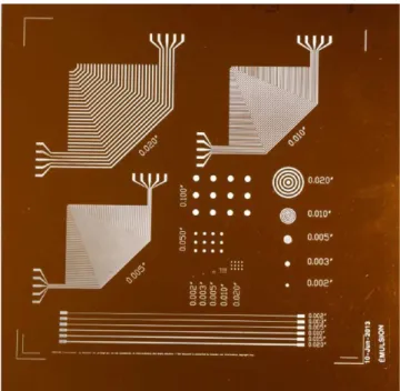
To take full advantage of printing some parts of electronic components with sufficient quality of printed traces sintering of the printed traces has to be well examined and