Publisher’s version / Version de l'éditeur:
Microelettronica e Beni Culturali, 2001
READ THESE TERMS AND CONDITIONS CAREFULLY BEFORE USING THIS WEBSITE. https://nrc-publications.canada.ca/eng/copyright
Vous avez des questions? Nous pouvons vous aider. Pour communiquer directement avec un auteur, consultez la première page de la revue dans laquelle son article a été publié afin de trouver ses coordonnées. Si vous n’arrivez pas à les repérer, communiquez avec nous à [email protected].
Questions? Contact the NRC Publications Archive team at
[email protected]. If you wish to email the authors directly, please see the first page of the publication for their contact information.
NRC Publications Archive
Archives des publications du CNRC
This publication could be one of several versions: author’s original, accepted manuscript or the publisher’s version. / La version de cette publication peut être l’une des suivantes : la version prépublication de l’auteur, la version acceptée du manuscrit ou la version de l’éditeur.
Access and use of this website and the material on it are subject to the Terms and Conditions set forth at
Integrated Optical Sensor for 3D Vision Systems
Gonzo, L.; Simoni, A.; Gottardi, M.; Stoppa, D.; Beraldin, Jean-Angelo
https://publications-cnrc.canada.ca/fra/droits
L’accès à ce site Web et l’utilisation de son contenu sont assujettis aux conditions présentées dans le site LISEZ CES CONDITIONS ATTENTIVEMENT AVANT D’UTILISER CE SITE WEB.
NRC Publications Record / Notice d'Archives des publications de CNRC:
https://nrc-publications.canada.ca/eng/view/object/?id=43c33593-0552-46cc-bf61-1015d62ff209 https://publications-cnrc.canada.ca/fra/voir/objet/?id=43c33593-0552-46cc-bf61-1015d62ff209Integrated Optical Sensor for 3D Vision Systems *
Gonzo, L., Simoni, A., Gottardi, M., Stoppa, D., Beraldin, J.-A.
April 2001
* published in Proceedings of the Progetto Finalizzato MADESS II.
Microelettronica e Beni Culturali. April 19, 2001. Florence, Italy. pp. 84-91. NRC 45803.
Copyright 2001 by
National Research Council of Canada
Permission is granted to quote short excerpts and to reproduce figures and tables from this report, provided that the source of such material is fully acknowledged.
84
A
BSTRACT
ACTIVE THREE-DIMENSIONAL VISION IS CONCERNED WITH EXTRACTING INFORMATION FROM THE GEOMETRY AND THE TEXTURE OF THE VISIBLE SURFACES IN A SCENE, REASONING ABOUT THE DATA AND FINALLY, COM-MUNICATING THE RESULTS. RECENT ADVANCES IN MICROELECTRONIC TECHNOLOGIES AND INTENSIVE RESEARCH ON INTEGRATED OPTICAL SENSORS HAVE OPENED THE WAY THE REALISATION OF COMPLEX ACTIVE RANGE CAM-ERA SYSTEMS. THIS PAPER WILL PRESENT THE EFFORT ON THE DESIGN AND DEVELOPMENT OF INTEGRATED CMOS OPTICAL SENSORS FOR ACTIVE THREE-DIMENSIONAL SYSTEMS BASED ON THE OPTICAL TRIANGULATION PRIN-CIPLE, CARRIED OUT AT ITC-IRST, IN COLLABORATION WITH THE NATIONAL RESEARCH COUNCIL OF CANADA (NRC).
Lorenzo Gonzo*, Andrea Simoni*, Massimo Gottardi*, Stoppa David* and J-Angelo Beraldin+
* ITC-Istituto per la Ricerca Scientifica e Tecnologica , I-38050 Povo Trento
+National Research Council of Canada, Ottawa, Ontario, Canada, K1A 0R6
Integrated optical sensor
for 3D vision systems
1. I
NTRODUCTIONThe desire to capture shape by op-tical means dates back to the begin-ning of photography. In the 1860’s François Villème invented a process known as photo sculpture, which used 24 cameras [1]. After a few years, however, as it was realised that the photo sculpture technique still need-ed a lot of human intervention, the idea was abandoned. It is only with the advent of computers that the process of capturing shape by optical means has regained substantial in-terest, more than 100 years later.
In the last twenty years many ad-vances have been made in the field of solid-state electronics, photonics, computer vision and computer graphics which have allowed the de-velopment of compact, reliable and
high accuracy 3D vision systems [2,3]. In particular advances in VLSI tech-nology and integrated sensor’s devel-opment help to accelerate the de-ployment of 3D vision systems in many fields like visual communica-tion, industrial automation and cul-tural heritage preservation. This latter field is one of the most stimulating as museum objects, paintings, archaeo-logical site features, architectural ele-ments and sculpture can be digitised to provide a high-resolution 3D digi-tal record of the object or site. The dig-ital record or “digdig-ital model” should provide archival quality documenta-tion which can be used for a variety of research, conservation, archaeo-logical and architectural applications, for fabricating accurate replicas as well as for interactive museum displays and Virtual 3D Theatre applications.
[INTEGRATED OPTICAL SENSOR FOR3D VISION SYSTEM]
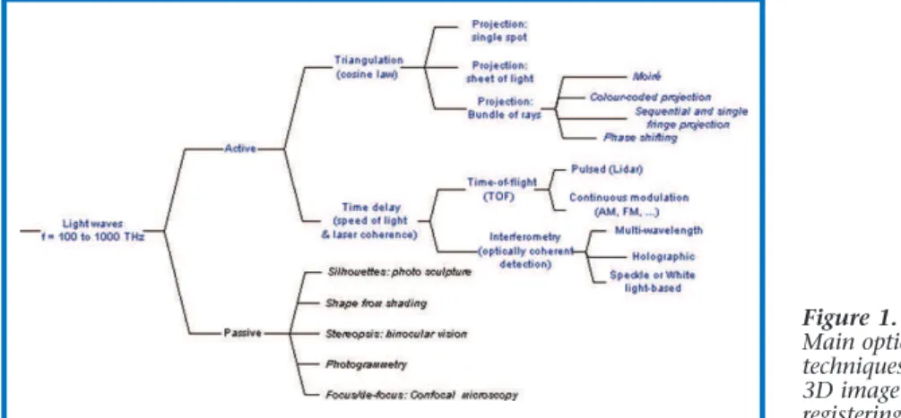
Figure 1 summarises all the known optical techniques that can be used to register three-dimensional im-ages. Depending on the measuring range, and on the required accuracy, some techniques may have advan-tages with respect to others. The clas-sification between active and passive techniques is due to the use or not of light sources helping the registration process. In our work we are mainly working with active techniques
which use coherent light sources like collimated laser or laser diode. As a rule of thumb long range applications (>5m) are better satisfied by time-of-flight (TOF) techniques, while trian-gulation is better for shorter ranges (5mm-5m). Within these latter, the development of integrated sensors for scanned single spot projection sys-tems is the subject of the work we present here.
The next section describes briefly
the measuring principle of a state of the art triangulator used to acquire depth maps with depth accuracy as high as 10mm over a depth of field of several centimetres. Section 3 deals with the description of the novel sen-sor we are proposing and whose ac-tual development stage is illustrated in Section 4. Conclusions follow in section 5.
2. T
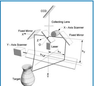
HE MEASURING PRINCIPLEA 3D surface map is captured by scanning a laser spot onto a scene, as shown in Figure 2, collecting the re-flected laser light, and finally
focus-ing the beam onto a linear laser spot
sensor. As the beam scans the scene
the spot moves continuously along the sensor, its position depending on the depth map. Geometric and pho-tometric corrections of the raw data give two images in perfect registra-tion: one with x, y, z co-ordinates and a second with reflectance data. In the figure the auto-synchronised scanner [2] is depicted schematically. Scan-ning of the laser beam is accom-plished by means of two high preci-sion electromechanical galvanome-ters each one supporting an appro-priate mirror. Notice that the mirrors are used both for projection and col-lection of the laser spot; this
Figure 1.
Main optical techniques for 3D image registering
86
[MICROELECTRONICS AND CULTURAL HERITAGE]
arrangement has the advantage of re-ducing the field of view and thus in-creasing the stray light immunity.
A laser beam composed of
multi-ple visible wavelengths might also be used for the purpose of measuring the colour map of a scene (reflectance map).
3. P
ROPOSED SENSORThe ITC-IRST and NRC groups are collaborating on a project that is tar-geted at the integration of key sensors used in the auto-synchronised scan-ner. These sensors include the
syn-chronisation photodiodes based on
bi-cells [4] which control the scanning pattern operated by the galvanome-ters, and laser spot position sensors [5] which detect the position of the spot as a function of the depth map. These sensors could become an integral part of future intelligent digitizers that will be capable of measuring accurately and simultaneously colour (re-flectance) and 3D. This, in turns, will accelerate the development of
hand-held 3D cameras [6] and multi-reso-lution random access laser scanners for fast search and tracking of 3D fea-tures [7]. All these digitizers will re-quire a thorough VLSI integration of basic laser camera functions to achieve size and cost reduction and most importantly, higher perform-ance.
Currently, commercial linear pho-todiode arrays used in 3D vision sen-sors are intended for 2D imaging ap-plications, spectroscopic instruments or wavelength division multiplexing in tele-communication systems. Their specifications change according to the evolution of their respective fields and not to digital 3D imaging. For in-stance, speckle noise dictates a large
Figure 2.Schematic
diagram of the NRC triangulator based on the auto-synchronised scanning technique.
[INTEGRATED OPTICAL SENSOR FOR3D VISION SYSTEM]
pixel size [8] that is not compatible with current 2D imaging develop-ments (where pixels are getting small-er). Many devices have been built or considered in the past for measuring the position of a laser spot more effi-ciently. Among those, one finds con-tinuous response position sensitive detectors (CRPSD) and discrete re-sponse position sensitive detectors (DRPSD) [9-10]. The category CRPSD includes lateral effect photodiode and geometrically shaped photo-diodes (wedges or segmented). A CRPSD
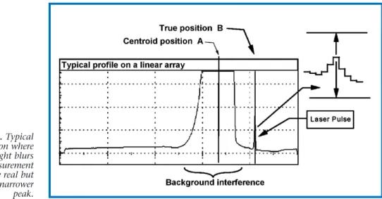
provides the centroid of the light dis-tribution with a very fast response time (in the order of 10 Mhz). DRPSD on the other hand comprise detectors such as Charge Coupled Devices (CCD) and arrays of photodiodes equipped with a multiplexer for se-quential reading. They are slower be-cause all the photo-detectors have to be read sequentially prior to the measurement of the location of the peak of the light distribution [7]. Fur-thermore, consider the situation de-picted on Figure 3, a CRPSD would
provide A as an answer. But a DRPSD can provide B, the desired response. This situation occurs frequently in re-al applications. The elimination of re-all stray light in an optical system re-quires sophisticated techniques that increase the cost of a system. Also, in some applications, background illu-mination cannot be completely elim-inated even with optical light filters.
We propose to use the best of both worlds. Theory predicts that a CRPSD provides very precise measurement of
the centroid versus a DRPSD [7]. By precision, we mean measurement
un-certainty. It depends among other
things on the signal to noise ratio and the quantization noise. In practice, precision is important but accuracy is even more important. A CRPSD is in fact a good estimator of the central lo-cation of a light distribution. On the other hand, DRPSDs are very accurate because of the knowledge of the dis-tribution but slow. Obviously, not all photo-sensors contribute to the
com-Figure 3.Typical
situation where stray light blurs the measurement of the real but much narrower peak.
88
[MICROELECTRONICS AND CULTURAL HERITAGE]
putation of the peak. In fact, what is required for the measurement of the light distribution peak is only a small portion of the total array. Hence the new smart detector. Once the perti-nent light distribution (after win-dowing around an estimate around the peak) is available, one can com-pute the location of the desired peak very accurately.
Figure 4 shows schematically the new smart position sensor for light spot measurement in the context of 3D and colour measurement. In a mono-chrome range camera, a portion of the reflected radiation upon entering the system is split into two beams (Figure 4.a). One portion is directed to a
CRPSD that determines the location of the best window and sends that infor-mation to the DRPSD. In order to meas-ure colour information, a different op-tical element is used to split the re-turned beam into four components, e.g., a diffractive optical element (Fig-ure 4.b). The white zero order compo-nent is directed to the DRPSD, while the RGB 1st
order components are directed onto three CRPSD which are used for colour detection (Figure 4.c). The CRPS-Ds are also used to find the centroid of the light distribution impinging on them and to estimate the total light in-tensity. The centroid is computed on chip for each colour with the well-known current ratio method i.e.
(I1-2 5 6 2 5 5 4 3 2 1 ....
Transmission grating or other splitting device DRPSD CRPSD a) Collecting lens Grating Red Green Blue White beam b) pb CDS control
Window start & pixel CDS Weighed average processor
control, registers, status DRPSD CRPSD pr pg Array reset Red spot Green spot Blue spot White spot c)
Figure 4.Description of the smart sensor for laser spot detection: a) in a monochrome system,
the incoming beam is split into two components, b) artistic view of a smart sensor with colour capabilities, and c) the proposed sensor.
[INTEGRATED OPTICAL SENSOR FOR3D VISION SYSTEM]
I2)/(I1+I2) where I1 and I2 are the cur-rents generated by that type of sensor [4]. The weighed centroid value is fed to a control unit that will select a sub-set (window) of contiguous photo-de-tectors on the DRPSD. That sub-set is lo-cated around the estimate of the cen-troid supplied by the CRPSD. Then, the best algorithms for peak extraction can be applied to the portion of interest.
4. I
MPLEMENTATIONAND EXPERIMENTAL RESULTS
We present here the architecture and preliminary experimental results of a first prototype chip of a DRPSD with selectable readout window. This is the first block of a more complex chip that will include all the compo-nents illustrated in Figure 4c. The prototype chip consists of an array of 32 pixels with related readout chan-nels and has been fabricated using a 0.8mm commercial CMOS process.
The novelties implemented consist in a variable gain of the readout chan-nels and an automatically selectable readout window of 16 contiguous pixels. Both features are necessary to comply with the requirements of 3D single laser spot sensors, i.e., a linear dynamic range of at least 12 bits and a high 3D data throughput. In the prototype, many of the signals, which, in the final system are sup-posed to be generated by the CRPS-Ds, are now generated by means of external circuitry. A diagram of the chip’s architecture is shown in Figure 5a. The array pitch is 50mm with each pixel having a sensitive area of
48 x 500 mm2
. The large dimensions of the pixel are required, on one side to cope with speckle noise [6] and, on the other side, to facilitate system alignment. Each pixel is provided with its own readout channel for par-allel reading. The channel contains a charge amplifier CA, and a
correlat-Figure 5.
Schematic diagram of the chip’s architecture
90
[MICROELECTRONICS AND CULTURAL HERITAGE]
ed double sampling circuit (CDS). To span 12 bits of dynamic range, the in-tegrating capacitor can assume five different values (CAP). In the proto-type chip, the proper integrating ca-pacitor value is externally selected. In the final sensor, however, the proper value will be automatically set by an on chip circuitry on the basis of the total light intensity as calculated by the CRPSDs. During normal opera-tion, all 32 pixels are first reset at their bias value and then left to integrate the light for a period of 10ms. With-in this time the CRPSDs and an ex-ternal processing unit estimate both the spot position and its total inten-sity and as calculated by the CRPSDs.
After that, 16 contiguous pixels, as addressed by the window selection logic, are read out in 52ms, for a total frame rate of 64ms. Future sensors will operate at full speed, i.e. an order of magnitude faster. The chip has been tested and its functionality proven to be in agreement with specifications.
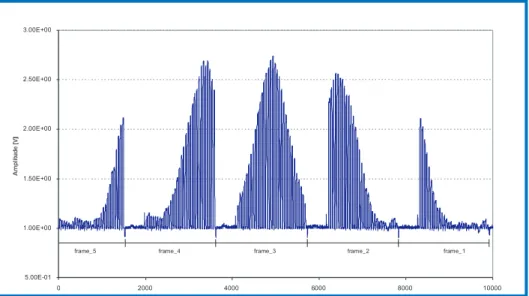
Figure 6 illustrates the functionality of the array as a laser spot is scanned on it. The scanning direction goes from right to left and progressive frames are read out from the sensor. The figure shows how the spot moves along the sensor and the good quality of the peak shape reproduction.
5. C
ONCLUSIONSThe results obtained in this work show the feasibility of integrated cus-tom optical sensors,Opto-ASICs, for complex applications like active 3D range cameras. The novel architecture of the linear sensor array proposed, when compared with the linear arrays currently used for such applications, introduces important improvements like fast readout through sub-win-dowing and high dynamic range (12 bits). Future developments concern the integration on chip of the DRPSD and the detection of colours.
5.00E-01 1.00E+00 1.50E+00 2.00E+00 2.50E+00 3.00E+00 0 2000 4000 6000 8000 10000 frame_1 frame_2 frame_3 frame_4 frame_5
Figure 6.Multi frame diagram of the chip response as a laser spot is scanner on the photosensitive
area.
[INTEGRATED OPTICAL SENSOR FOR3D VISION SYSTEM]
R
EFERENCES1. B. Newhall, “Photosculpture”, Im-age, 7(5), (1958), pp.100-105, 2. M. Rioux, “Laser Range Finder based
on Synchronized Scanners”, Appl. Opt., 23, (1984), pp. 3837-3844, . 3. J.-A. Beraldin, F. Blais, L. Cournoyer,
M. Rioux, S.H. El-Hakim, R. Rodella, F. Bernier and N. Harrison, “3D Digi-tal Imaging and Modeling on Re-mote Sites”, Proc. Second Intern. Conf. on 3D digital imaging and modelling, Ottawa, Canada, (1999). 4. L. Gonzo, M. Gottardi, A. Simoni,
and J.-A. Beraldin, “A novel optical bi-cell integrated readout circuitry,” Proceedings of the 1999 IEEE Inter-national Symposium on Circuit and Systems, Orlando, FL. May 30-June 2, (1999).
5. L. Gonzo, A. Simoni, M. Gottardi, D. Stoppa , “Smart Sensors for 3D
Digi-tization”, Proceedings IEEE
Instrumen-tation and Measurement Technology Conference (IMTC), Budapest,
Hun-gary, (2001).
6. Hébert, P. and Rioux, M., Toward a hand-held laser range scanner: inte-grating observation-based motion compensation, IS&T/SPIE’s 10th In-tern. Symp. Electronic Imaging, 24-30 Jan., (1998)
7. J.-A. Beraldin, F. Blais, M. Rioux, L. Cournoyer, D. Laurin, and S.G. MacLean, “Eye-safe digital 3D sens-ing for space applications,” Opt. Eng. 39(1), (2000), pp. 196-211 8. R. Baribeau, and M. Rioux,
“Influ-ence of Speckle on Laser Range Find-ers,” Appl. Opt., 30, (1991), pp. 2873—2878, .
9. A. Makynen and J. Kostamovaara, “ Linear and Sensitive CMOS position sensitive photodetector” El. Lett., 34, (1998), pp. 1255-1256.