HAL Id: hal-01843388
https://hal.archives-ouvertes.fr/hal-01843388
Submitted on 18 Jul 2018
HAL is a multi-disciplinary open access archive for the deposit and dissemination of sci-entific research documents, whether they are pub-lished or not. The documents may come from teaching and research institutions in France or abroad, or from public or private research centers.
L’archive ouverte pluridisciplinaire HAL, est destinée au dépôt et à la diffusion de documents scientifiques de niveau recherche, publiés ou non, émanant des établissements d’enseignement et de recherche français ou étrangers, des laboratoires publics ou privés.
Novel 3D back-to-back diodes ESD protection
Bertrand Courivaud, Nicolas Nolhier, G. Ferru, Marise Bafleur, Fabrice
Caignet
To cite this version:
Bertrand Courivaud, Nicolas Nolhier, G. Ferru, Marise Bafleur, Fabrice Caignet. Novel 3D back-to-back diodes ESD protection. Electrical Overstress/Electrostatic Discharge (EOS/ESD) Symposium , Sep 2014, Tucson, AZ, United States. 4p. �hal-01843388�
1
Novel 3D back-to-back diodes ESD protection
B.Courivaud (1,2,3), N.Nolhier (1,2), G.Ferru (3), M.Bafleur (1,2), F.Caignet (1,2)
(1) CNRS, LAAS, 7 avenue du Colonel Roche, F-31400 TOULOUSE, FRANCE tel.: +33561337840 , e-mail: rbeges@laas.fr
(2) Univ. de Toulouse, UPS, LAAS, F-31400, Toulouse, France (3) IPDIA, 2 Rue de la girafe, 14000 Caen, France
A 3D technology is used to design ESD protection devices. Based on back-to-back diodes, these devices are dedicated to first stage, external ESD protection. The main feature consists in using deep trenches, usually employed to build capacitors, to design 3D diodes. Specific trench configuration improves cumulative ESD stress robustness.
I. Introduction
Usually external ESD protection doesn't require a high surface area optimization as IC's ESD protection. But for applications where the protection and the device are reported on the same substrate, surface area should be minimized. The main goal of this study is to demonstrate the functionality of 3D diodes as ESD protection and to estimate the impact of surface reduction regarding conventional diodes. The technology process is based on an existing one developed by IPDIA [1][2] for the design of high values capacitors. During an etch step, some holes are drilled in the silicon and then filled with polysilicon. In this particular case, the deposited polysilicon is doped with high phosphorus active concentration. After a thermal diffusion, we obtain a three dimensional diode including several holes connected in parallel. Back- to-back diodes are obtained by duplicating the 3D diode as depicted in Figure 1.
Figure 1: Scheme of 3D back-to-back diodes.
The back-to-back configuration deviates the E S D current when the voltage at the protection electrode
exceeds their breakdown voltage. A typical electrical implementation scheme is shown on Figure 2. The component is fully symmetrical i. e. the device protection is guaranteed for positive and negative ESD discharge.
Figure 2: Typical implementation of external 3D back-to-back diode protection.
The clamping voltage could be tuned in the range of 10V to 80V by changing technological parameters.
II. Layout parameter variations
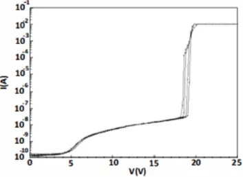
In order to optimize ESD protection robustness we have studied two layout parameters (Figure 1): the distance (DIP) between holes and the distance between the two diodes (DID). As we decided to keep the same active surface area for each diode, the smallest distance between holes increases their quantity per diode (from 310 to 5700). A first study was carried out to determine the impact of this parameter on the breakdown voltage. From Figure 3, we can see that regardless of the number of holes, the
2
leakage current is very steady and the breakdown voltage is roughly the same ( l9V).
The second parameter variation is the distance DID which has been varied from 35 to 165µm. We assumed that a trade-off has to be found between the current homogeneity during an ESD discharge and the device density impacted by a larger distance between diodes.
Figure 3: DC curves for several DIP lengths.
As in the previous case, for all these devices no significant breakdown voltage variations have been found.
III. TLP results
To study the device ESD robustness, we
performed a Transmission Line Pulsing
characterization (TLP). The TLP stresses are increased until the device exhibits a leakage current equal to lµA, corresponding to IT2. From the measured
results presented in Figure 4, we can observe that IT2
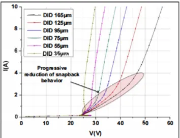
increases with the number of holes. For large DIP distance, each hole can be considered as an elementary diode, so when more and more holes are used, the current density in each hole is lowered, and the ESD robustness is improved. This behavior saturates when we reach 2100 holes because the holes diffusions touch each others, creating a mega junction. The results demonstrate that the interdiode distance DID is also impacting the structure ESD robustness. When DID is increased, the intrinsic resistance of the device is increased too which should degrade ESD robustness in terms of power dissipation. But, as this added resistance acts as a ballast resistance, the resulting on-resistance of the device during ESD is lowered because current flow distribution is more uniform. DID have an optimum value. A good trade- off between ESD robustness and surface area is found
for a device formed by 5700 holes with a 95µm DID length. IT2 is 22A, corresponding roughly to 33kV
HBM robustness. Total layout area of the structure is 160,000µm2.
Figure 4: TLP curves: IT2 versus number of holes for different DID values.
The hypothesis regarding the creation of mega junction has been verified. Cross sections of the devices have been prepared with a FIB setup and after a revelation step, the phosphorus diffusion behavior have been highlighted.
Figure 5: Cross section of holes with phosphorus diffusion view.
On the picture 5, the DIP distance is sufficiently large to form separated holes. But for lower DIP distance we found lower limit before holes touch each other. This distance is approximately twice the width of a hole. However in a specific combination of DID and DIP values, the device exhibits a surprising behavior. Figure 6 shows that at high current stress of l0A, a first hole is damaged. But as the holes are in parallel, this latter fuses, and the rest of the structure is still functional up to 16 A with a reasonable leakage current (below lilA). So, if the maximum leakage current allowed by the protected power ICs, is below
3
100µA, the device has a good reliability regarding cumulative ESD stress.
Figure 6: showing small impact of failed holes on the increasing leakage current.
IV. TCAD Analysis
To understand the behavior of the device investigated, a study has been carried out with TCAD simulation tools. Several assumptions were chosen for the simulator parameters. Thermal models have been neglected. In case of evaluating thermal breakdown this assumption should be critical but, in our case, we want only to highlight the difference in current distribution from a device to another. The purpose of the simulations is not to find IT2. The benefit is to
provide a good simulation convergence and avoid the limited thermal validity (600K-800K) of the impact ionization models [3].
Figure 7: Doping concentration distribution of studied device.
During TLP measurements, the I-V curve is constructed by extracting, for a given pulse, the current and voltage of device under test between 70 and 80 ns. We consider that during this time slot stationary regime is achieved. Based on this assumption high current simulations are performed using ACS technique [4]. A single current ramp (10A, l00ns) is applied to the device rather than using several TLP pulses. The numerical calculation exhibits a better convergence and a great computational time speed-up. The major drawback of this method is a possible overvoltage during device triggering that could not be detected [5]. The third
assumption has been chosen regarding the structure geometry. A complete structure description is very complex and would lead to a huge structure mesh. We chose to perform bi-dimensional simulation with a limited number of holes (10) for each diode, as shown on Figure 7. For the total current calculation, an area factor has been tuned to fit the real device configuration.
A. DC Analysis simulations
A first simulation set has been performed in DC analysis to extract the breakdown voltage and calibrate the simulator. The impact of DID distance have been also studied. As reported in Table 1 the breakdown voltage is roughly the same irrespectively of the DID distance. Its value is slightly higher than the DC measurement. This can be explained by a little mismatch on doping profile description.
Table I: DC curves simulation for several DID distances.
B. High current simulations
The measurement results in Figure 4 have shown that the ESD robustness is dependent on the DID distance between the two back-to-back diodes. When this distance increases, IT2 increases too but exhibits saturation for DID largest values.
Figure 8: Anodes current distribution for several DID lengths.
Even if it is not possible to extract IT2 from the simulations, the impact of DID values on the current distribution in all the holes have been studied.
Figure 8 shows the current distribution in each hole of the reversed biased diode for a total current of
4
10A. For the shortest DID distance, it is clear that the anode connected to the first hole, A I, carries the major part of the current because it is the closest hole to the forward biased diode that acts as a cathode, or an emitter if we consider the total device as a bipolar transistor with a floating base. This behavior remains for higher DID value but is attenuated. A higher DID distance induces, between the diodes, a higher serial resistance t h a t tends to attenuate the added current path from hole A1 to hole A10. This latter exhibits a surprising behavior. Even if it is located farther from the cathode, simulations show an increase of the current for this hole compared to neighboring holes (A9 or A8). This is due to the cylindrical junction created by the last trench. The current will predominantly flow towards the front anodes but will also be better distributed to the rear ones. This phenomenon must be taken into account to optimize the ESD robustness.
Figure 9: High I-V curves for several DID lengths.
High current versus voltage curves are presented in Figure 9. It shows that the on-resistance of the device in high current mode is increased with the DID distance, as discussed before. We can also notice that there is for each curve two different slopes. Roughly the device has two on-resistance values. Considering the lowest DID value, 35µm, the I-V curve presents a negative resistance between 200 mA and 600 mA. It is a snapback effect caused by impact ionization generated by the high electric field in the high concentration P layer. Due to this high electric field the electron hole pairs are drifted apart of the other direction. Consequently, the potential barrier height is reduced and the voltage drops too. This phenomenon appears when the P concentration is higher than 1017
at/cm3 [6]. If the DID distance increases, the higher series resistance between diodes compensate this
snapback effect. Of course, a trade-off must be found between ESD robustness, device surface area and ESD protection design window. As shown in Figure 9, if the DID distance is large, the sustained voltage for high current is very high, and the ESD protection would not be efficient.
V. Layout optimization strategy
A. Trench optimization
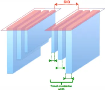
With the aim to optimize ESD structure robustness, a novel layout of our device has been designed. As seen previously, a specific DIP distance leads to holes touch each others with diffusion. Consequently, the emerging first idea has been to replace the holes by trenches along the length of the diode. The main advantage of trench is that we can benefit of more degrees of freedom for etching process. Then, with this particular feature, etching is deeper.
Figure 10: Scheme of 3D back-to-back Trench diodes.
Further, in the trenches, the doping concentration is the same at all point of this plan junction length and there is no more resistance variation.
5
Figure 11 shows the cross section of trench diode. All these trenches have the same depth. One can observe that the trenches are not completely filled with polysilicon. Actually, the top of the trench is filled faster than the middle, and a cavity is formed along it. But we assume that there is no electrical impact because the doping diffusion is continuously present from the top to the bottom of the trench. Furthermore, these cavities should not pose a reliability issue for the device because they are totally encapsulated.
B. Width trench modulation
We have observed in paragraph III that the weakness of the previous device is the first line of holes. TCAD results in paragraph IV have also shown for high current density, that the major part of current flow through first holes. All current is carried by them and consequently device is failed. This phenomenon is exactly the same for trench structure and a new design has to be found in order to achieve a better current homogeneity in the diode. To have a better current distribution along the width of the diode, we need to decrease progressively the resistivity of each trench and adapt it as a function of the distance. This can be done by gradually increasing the trenches width. This width modulation offers another benefit. During the etching step, chemical species have an easier condition to penetrate in trenches. Consequently trenches are deeper in silicon substrate as we can see in the figure 12.
Figure 12: Scheme of 3D back-to-back trench diodes with width and depth modulation.
This depth modulation of trenches will result in silicon intrinsically by a decrease of on-resistance.
Indeed, as trenches are deeper at the rear, the distance traveled by the current is smaller in comparison with last trench device and the on-resistance in substrate is reduced. The particularity of this component resides on the self-compensation of the resistance of the substrate as shown in Figure 13.
Figure 13: Schematic of conductivity compensation resulting into modulation of trench width.
Figure 14 shows a cross-section of a device with a trench modulation of 300nm. As expected last trench is deeper than the first one. But this variation of 5 urn is not very significant. However we can imagine that if we take larger trenches, the corresponding depth is significant. We cannot define a fixed step of this depth modulation because the relation between the trench width and depth is not linear.
Figure 14: Cross section of trench diode with 300nm step width.
C. High current simulations
To confirm the previous hypothesis on current distribution in the structure, a TCAD simulation was performed under the same condition as explained in paragraph IV. The number of trenches has been limited to 10 for mesh consideration as depicted in Figure 15. The current distribution in the trenches has been plotted in figure 16 vs several DID distances.
6
Figure 15: TCAD current density calculation in a 3D device for a fixed l0A TLP stress.
The simulation offers a trench width modulation of 0.5µm between two adjacent trenches. The injected TLP stress is fixed to l0A. We can compare TCAD results between figure 8 and figure 15. For the same total current injected in the component, a major part of the current is also carried by the first anode. However, for trenches A6 to A l0 we can see a different behavior.
Figure 16: Anodes current distribution for several DID lengths.
Whatever DID distance, the phenomenon is the same. The trench width modulation technique leads to a current distribution. If we look closely to DID 165µm curve, current in first anode is reduced (30%) and the current level in the rear trench is almost the same. The combination of ballast resistance due to large DID distance and the conductivity modulation induces current levels upstream and downstream positions in structure to be approximately the same.
VI. New TLP measurements
To demonstrate the efficiency of width modulation on ESD protection devices robustness, a study was carried out for different topology. For the
same surface diode area (S-diode) of 4032µm2, three
DID distance 55µm, 75um and 95um allow to have three corresponding total surface area (S-total) as above on the figure 17.
Figure 17: Layout view with the different surface diode.
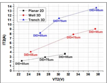
Figure 18: IT2-VT2 curves for Planar2D, Well3D and Trench3D back-to-back diode and for several DID lengths
This clearly shows that 3D technology is more robust than 2D's. Whatever DID distance Well3D robustness is approximately twice of Planar2D configuration, which is about 6kV HBM. If we focus now on 3D technology, we see directly than our first hypothesis on using simple trenches to improve surface junction area was a sound idea. We obtain a better robustness compared to well topology. IT2 is
13.7A corresponding of 20.5kV HBM robustness against 13.6kV for Well3D device. This increase is about 50%. The homogeneous doping concentration of first trench representing the main junction area gives a better current conductivity at on state.
7
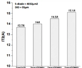
Figure 19: Bar-chart of IT2 for several step trench modulation
width.
However, like Well3D we wanted to know in the same figure, the impact of DID distance on IT2 for Trench3D device. The change curve slope indicates us there is also a limit of this distance where IT2 stop to increase. The phenomenon is exactly the same for Well3D structure but this time, for a different current level. As previous seen on simulation, it would appear that the trench width modulation has also non-neglect impact. The current density must be more homogenous along trenches and should increase ESD robustness. Furthermore, increased trench width with the distance should also improve on-state resistance RON thanks to the change of depth trench. In the results shown below we wanted to quantify the impact of this modulation for different modulation width step. This step goes 100 nm to 300 nm but does not at the moment permit to give information on corresponding depth.
Figure 20: IT2 versus S-diode for 100 nm step width modulation
and three DID distance.
From Figure 19, we see that a larger trench gives even better results in terms of ESD robustness. It is important to detail that V T2 is similar for all configurations (VT2=37 to 38V).
As seen on the Figure 20, for the same step width modulation about 100nm, doubling surface diode area gives better results. It's interesting to see that the evolution of robustness is the same whatever DID distance. This phenomenon should be kept up to a certain value of DID. When DID is 95um we can see there are not a large variation between the two diode's area. This hypothesis seems to be true.
VII. Conclusion
This work presented a novel 3D back-to-back diode ESD protection in a technology process dedicated to manufacturing high value capacitor. An etch step, necessary to form the capacitor, is used to produce three-dimensional elementary diodes. These elements are combined to form the back-to-back diode. This structure is appropriate to external, first stage, protection for high voltage ICs. Combining in the same component, high capacitors for filtering or decoupling, and efficient ESD protection, is a great challenge in system-level consideration. This study is based on experimental measurement on several test vehicles but also on TCAD simulations to better understand the device behavior in high current regime. The impact of layout variations on ESD robustness is also studied. The study has separated in three parts: first, 3Dwell back-to-back diode are investigated and two major parameters have been analyzed: the distance between the holes, and the distance between the two diodes. For a silicon surface area about 160 000um2, the best trade-off provides 33kV HBM robustness for the targeted ESD protection design window. For a surface silicon area of 30,000um2, Planar2D back-to-back diode robustness is low and doesn't exceed 6kV HBM robustness. Secondly, a new device configuration which replaces well by trench polysilicon has been investigated. This preliminary study has shown that for the same silicon surface area, device provides 20.5kV HBM robustness against only 13.6kV for Well3D device corresponding to an increase about 50%. Finally, to optimize this ESD protection device, a new emerging idea has been explored consisting to modulate trench width with many stepwise. The best configuration permits to have 22.7kV HBM robustness.
8
References
[1] F. Murray, "Silicon based system-in-package: a passive integration technology combined with advanced packaging and system based design tools to allow a breakthrough miniaturization", IEEE-BCTM, pp. 169-173, 2005.
[2] S. Gaborieau, C. Bunel, F. Murray, "3D Passive Integrated Capacitors Towards Even Higher Integration", IMAPS 2010.
[3] C. Salamero, N. Nolhier, M. Bafleur and P. Besse, "Accurate prediction of the ESD robustness of semiconductor devices through physical simulation", IEEE-IRPS, pp 115-8, 2005.
[4] Galy et al. "Numerical evaluation between Transmission Line Pulse (TLP) and Average
Current Slope (ACS) of a submicron gg-NMOS transistor under Electro-Static Discharge (ESD)", Workshop EOS/ESD/EMI, p. 15-22, 2002.
[5] A. Delmas, A. Gendron, M. Bafleur, N. Nolhier and C. Gill, "Transient voltage overshoots of high voltage ESD protections based on bipolar transistors in smart power technology", IEEE-BCTM, pp253-256, 2010.
[6] Yu Bin, King Ya-Chin, Pohlman J., "Punchthrough transient voltage suppressor for EOS/ESD protection of low voltage IC's", Electrical Overstress/Electrostatic Discharge (EOS/ESD) Symposium Proceedings, 1995, pp. 27-33.