Low-loss buried AlGaAs/AlOx waveguides using a quasi-planar process
Texte intégral
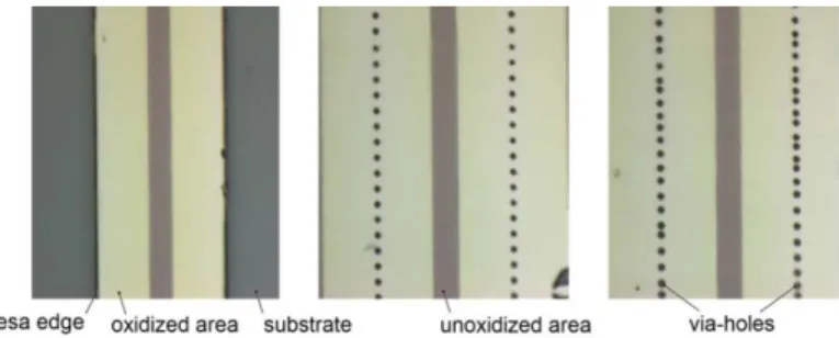
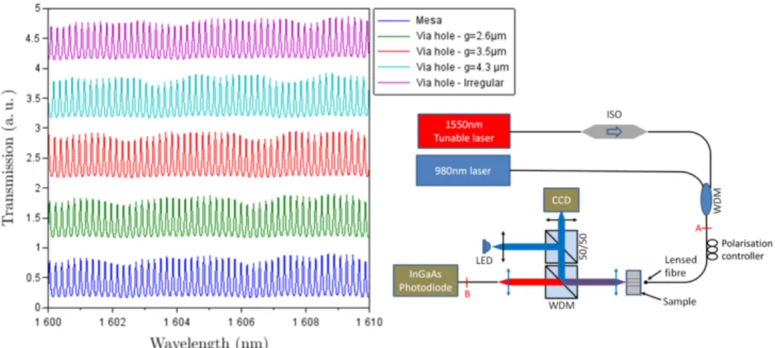
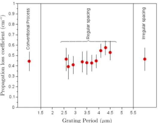
Figure
Documents relatifs
Achieving a secure federation of mobile devices calls for a framework and mechanisms that allow the specification and enforcement of security policies across different trust
Prompted by claims that garbage collection can outperform stack allocation when sucient physical memory is available, we present a careful analysis and set
Implicite- ment, le Traité de la CEDEAO sur la libre circulation des personnes a conféré un statut particulier aux res- sortissants ouest-africains qui émi- grent dans les
This document lists the various Voice Profile for Internet Mail (VPIM) email address formats that are currently in common use and defines several new address formats for
level), when an adjacency reaches the "UP" state, the starting router starts a timer T1 and transmits an IIH containing the restart TLV with the RR bit clear and SA
Because I was using Kerberos authentication, I was able to log into cfs without typing a password; instead, my telnet client obtained a service principal from the Ticket
New chapters include coverage of important topics like VoIP and EAP Coverage of cutting edge technologies like optical networking and storage Authored by Cisco Systems, worldwide
Allows input of an entire matrix from the teleprinter; a new working size may be specified, within the limits of the DIM statement on total number of
