Charge and Exciton Dynamics in Quantum Dot
Light-Emitting Diodes
by
Han Zhu
B.S.E., Electrical Engineering
Princeton University (2011)
MASSACETTNSTYTUTEOF TECHNOLOGY
JUL 24
2019
LIBRARIES
ARCHIVES
Submitted to the Department of Physics
in partial fulfillment of the requirements for the degree of
Doctor of Philosophy in Physics
at the
MASSACHUSETTS INSTITUTE OF TECHNOLOGY
June 2019
@
Massachusetts Institute of Technology 2019. All rights reserved.
Signature redacted
Author ...
Signature
De artment of Physicsredacted
24, 2019
C ertified by ...
...
Vladimir Bulovid
Professor of Electrical Engineering and Computer Science
S ig nature
red
acted
Thesis Supervisor
Certified by
...
Leonid Levitov
Professor of Physics
Thesis Supervisor
Accepted by...
Signature redacted
Nergis Mavalvala
Associate Department Head of Physics
Charge and Exciton Dynamics in Quantum Dot
Light-Emitting Diodes
by
Han Zhu
Submitted to the Department of Physics on May 24, 2019, in partial fulfillment of the
requirements for the degree of Doctor of Philosophy in Physics
Abstract
Colloidal quantum dot based light-emitting diodes (QD-LEDs) offer the possibility of bright, saturated, and tunable emission for the next generation of display and solid-state lighting technologies. In this thesis, we study how the interplay of charges and excitons in a QD-LED affect its operational behavior.
In order to construct a physical model of a QD-LED, we start by developing quantitative characterization methods that directly measure charge accumulation and electric field in an operating device. Comparison of measured internal device variables with observed electroluminescence and current density allows us to disentangle the deleterious effects of charge imbalance, electric field, and Joule heating on the external quantum efficiency. We also find that the magnitude of electron accumulation on the
QD film is sensitive to its interface with the neighboring hole transport layer (HTL)
and can reach nearly one electron per QD even in the best performing device. We next investigate how exciton formation is affected by the high charge density. Since the degree of electron charging of a nanocrystal shifts the energy barrier for hole injection, the kinetics of exciton formation are dependent on electron occupation statistics on the QD film. Using kinetic Monte Carlo simulations that explicitly incorporate both long and short range Coulomb interactions, we find that energetic disorder of the QD film strongly enhances the formation of negatively charged excitons
by increasing the population of two-electron occupied QDs.
Finally, we demonstrate that the photoluminescence yield of a QD film can be intentionally quenched by up to 99.5% in a QD-LED under reverse bias. This paves the way for a voltage-tuned optical down-conversion device using colloidal QDs. Thesis Supervisor: Vladimir Bulovid
Thesis Supervisor: Leonid Levitov Title: Professor of Physics
Acknowledgments
Sitting at the desk closest to Prof. Vladimir Bulovi6's office for past six years, I could
not help but be continuously affected by his joyous, resounding laughter that rebounds off my office door before travelling all the way down the building. I deeply appreciate his infectious enthusiasm for both scientific and engineering research, which always reinvigorated my own whenever my spirit was dampened by technical minutia. I am grateful not only for his patience as I only very gradually discovered focus on the projects that comprise this thesis, but also for the freedom he provided in allowing me to avoid device fabrication altogether through all these years. I would also like to thank Prof. Leonid Levitov, Prof. Marin Soljacic, and Prof. Janet Conrad for kindly serving on my thesis committee.
A majority of this thesis is made possible only by collaboration with other QD-LED team members in ONE Lab. I am especially indebted to Giovanni Azzellino,
Matthew Chua, Jonas Xie, and Melissa Li, who have all very promptly provided me with batches upon batches of devices to test as I continuously destroyed them in the optics lab. I also appreciate the discussions I had with Yasu Shirasaki and Geoffrey Supran when I first joined the group, whose ideas and earlier work on QD-LED device physics repeated show up in this thesis. I would also like to thank collaborators in Prof. Moungi Bawendi's group, Jason Yoo and Michel Nasilowski, for providing the
QD
and Zno nanoparticles for the devices.Beyond collaborators on QD-LED work, I want to give special acknowledgement to Tom Mahony, with whom I had many insightful discussions on either technical problems in the optics lab, or to flush out fledgling ideas that I often became con-fused about. Thank you for being a good friend and office mate, for installing the hangboard, for the climbing discussions, and the physical labor in building the MIT climbing wall! I also must give a shout out to the friendship and support by all the other members of ONE Lab and associates, especially Farnaz Niroui, Wendi Chang,
Joel Jean, Joel Yuen, Brian Modtland, Richard Swarthout and other former occu-pants of the Best Office, and Mengfei Wu and all of the fellow group meeting food Czars.
My first two years at MIT was spent in Quanta group, and I sincerely thank Prof.
Isaac Chuang for giving me the opportunity to work on ion trap projects, as well as instilling in me the willingness to take on unfamiliar hardware challenges. I would like to thank former Quanta members Helena Zhang, Guanghao Low, Theodore Yoder, and Michael Gutierrez for their friendship, game nights, and for allowing me to borrow lab equipment over the next six years!
Beyond the lab, I must thank Greg Dooley, who was a wonderful housemate for over five years. I also need to thank Aakash Ravi, Liane Bernstein, Hank Song, and Carlos Sandoval, who, through our climbing trips, injuries and sufferings, failures and successes, have enriched my grad school life and fueled an obsession.
And finally, thank you to my fiancee Amira Eltony: your love, support, patience as I struggled, tolerance as I vented, understanding as I obsessed, are all I could ever ask for. Thank meow to Molly and Batcat, whose fluff I have by now spread to every corner of the lab, and whose cuddles may or may not have slowed down the writing of this thesis. And thank you to my parents, whose care, support, and advice helped me every step of the way though the long graduate school days.
Contents
Cover page Abstract Acknowledgments Contents List of Figures 1 Introduction1.1 Quantum Dot Light Emitting Diodes . . . .
1.2 Thesis O utline . . . .
2 Colloidal Quantum Dots and Light Emitting Diodes
2.1 Colloidal Quantum Dots . . . . 2.1.1 Electronic Properties . . . . 2.1.2 Optical and Electronic Processes . . . . 2.2 Quantum Dot Light Emitting Diodes . . . .
2.2.1 Structure of QD-LEDs . . . .
2.2.2 Efficiency Loss Mechanisms . . . .
7 -A 1 3 5 7 11 15 17 18 19 19 19 25 30 30 32
3 Direct Measurement of Charge and Electric Field in a Quantum Dot Light Emitting Diode
3.1 Survey of Optical Characterization Techniques ...
3.2 Our Approach ...
3.3 Device Structure and Measured Quantities . . . .
3.4 Differential Absorption Spectroscopy . . . .
3.5 Measurement of Absolute Charging . . . . 3.6 Extraction of Charge and Field . . . . 3.6.1 Interpretation of differential absorption spectra
3.6.2 Systematic errors for extracted electric field . .
3.7 Time-resolved photoluminescence . . . . 3.8 Charge Transport and Charge Balance in QD-LED 3.9 Effect of Charging on External Quantum Efficiency 3.10 Effect of Electric Field on EQE . . . . 3.11 Conclusion . . . ... . . . .
4 Kinetic Monte Carlo Modeling of a QD-LED
4.1 Overview of Kinetic Monte Carlo Methods . . . . 4.2 Challenges to modeling devices with nanostructured material . . . . . 4.3 High level description of simulation . . . . 4.4 Lattice generation . . . .
4.4.1 Molecular Dynamics Simulation of Organic Thin Film
Morphol-ogy... ... 4.4.2 Morphology of QD films . . . . 4.5 Computational optimizations . . . . 4.6 V alidation . . . . 8 35 . . . . 36 . . . . 38 . . . . 40 . . . . 43 . . . . 47 . . . . 48 . . . . 48 . . . . 51 . . . . 53 . . . . 59 . . . . 63 . . . . 67 . . . . 70 73 73 74 77 80 81 82 83 84
5 Exciton Formation at Nanocrystal/Organic Semiconductor
Hetero-junction
Coulomb interactions and disorder . . . .
Equilibrium Thermodynamics near QD/organic Interface Kinetic Monte Carlo Methods . . . . Energetic Disorder . . . . Barrier height and Electric Field effects . . . . Interface Morphology . . . . Implication for Devices . . . . Conclusions . . . . . . . . 87 . . . . 92 . . . . 95 . .. .. . 99 . . . 103 . . . . 106 . . . . 108 . . . . 110
6 Electrically-Controlled Near Complete Quenching of Quantum Dot Photoluminescence 113 6.1 Introduction ... ... 113
6.2 Electric field effects in quantum dots .... ... 114
6.3 Our approach ... ... 117
6.4 Device Performance . . . . 118
6.5 Principles of Operation . . . . 124
6.5.1 Electroabsorption . . . . 124
6.5.2 Characterization of Quenching Mechanisms . . . . 125
6.5.3 Investigating Slow Charging Dynamics . . . . 129
6.6 Discussion and Conclusion 7 Summary and Outlook 7.1. O utlook . . . . 132 135 137 A Details on differential absorption and simultaneous electrolumines-cence/photoluminescence measurements 139 A.1 System Overview . . . . 139
9 -1 5.1 5.2 5.3 5.4 5.5 5.6 5.7 5.8 6.
A.2 Balanced Photodetector . . . 141
A.2.1 Power Supply . . . 149
A.2.2 Temperature Control . . . 150
A.2.3 DAC
/
Reference source . . . 151A.2.4 Other Noise Sources . . . 151
B QD-LED Fabrication Details 153 B.1 Colloidal quantum dot synthesis . . . 153
B.2 Synthesis of ZnO nanoparticles . . . 155
B.3 Device fabrication . . . 156
Bibliography 159
List of Figures
2-1 Electronic structure of bulk CdSe and photograph of colloidal QDs 20
2-2 Structure, photograph, and energy band diagram of QD-LED . . . . . 31
2-3 Schematic illustrations of different loss mechanisms in a QD-LED . . 34
3-1 Cross-sectional TEM, energy-band alignment, and spectrum of a QD-LED, as well as schematic of optical characterization setup. . . . . 39
3-2 Representative differential absorption spectra of a QD-LED under
for-ward and reverse bias, as well as of a capacitor structure under forfor-ward b ias. . . . . 4 2
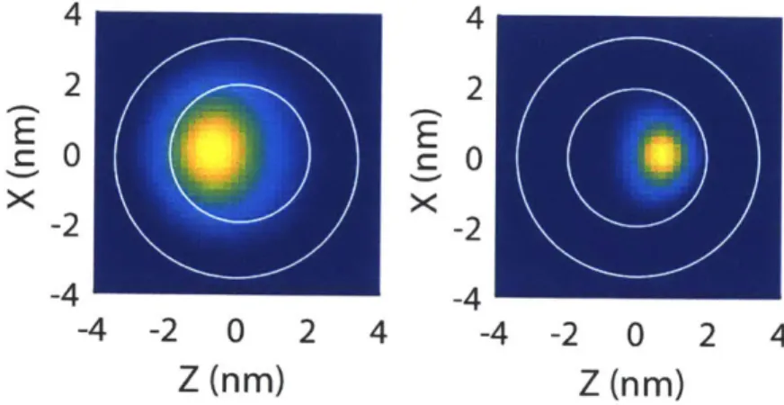
3-3 Stark spectrum amplitude vs QD thickness. . . . . 44
3-4 Calibration of absorption spectra bleach using capacitor structures. 46
3-5 Electron and hole wavefunctions in a QD-LED under electric field. . 52
3-6 Energy shift of neutral and negatively charged exciton under an electric
field . . . . 53 3-7 TRPL of QD-LED under forward bias. . . . . 54
3-8 Fitting of TRPL traces. . . . . 55 3-9 Simulated TRPL traces with different FRET rates and electron densities. 58 3-10 Electron occupation, electric field, voltage drop over the HTL, and J-V
curves of a QD-LED under forward bias. . . . . 61
3-11 EQE, charge-efficiency frontier, and EL spectra of QD-LEDs in operation. 64
3-12 Photoluminescence of QD-LEDs in operation. . . . . 68
3-13 Simulated PLQY of QD film at various electron occupancy. . . . . 70
4-1 Flow chart outlining the algorithm of a typical KMC simulation. . . . 78
4-2 Molecular structure and morphology of typical HTL materials. . . . . 81
4-3 Simulated mobility of amorphous organic molecular film. . . . . 85
5-1 Ratio of formation rate of negative trions to neutral excitons, as esti-mated from the non-interacting partition function. . . . . 91
5-2 Output of a typical KMC simulation. . . . . 96
5-3 Relative formation rate of charge excitons, extracted from KMC sim-ulations. . . . . 100
5-4 Effect of electric field on relative formation rate of negatively charged excitons. . . . . 104
5-5 Relative formation rate of negatively charged excitons for a rough QD/HTL interface. . . . . 107
6-1 Energy band alignment of QD-LED under reverse bias. . . . . 118
6-2 J-V, EQE, luminance, and EL spectra of QD-LED under forward bias. 119 6-3 PL spectra, intensity, and peak wavelength of under reverse bias.. . . 120
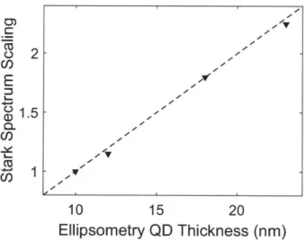
6-4 CCD images of PL quenching in a QD-LED under reverse bias. . . . 122
6-5 Transient behavior of PL quenching in a QD-LED on second and nanosecond time scales. . . . . 123
6-6 Electroabsorption spectrum of QD film, measured in a QD-LED under reverse bias. . . . . 124
6-7 TRPL curves of QD films in a QD-LED under reverse bias. . . . . 125
6-8 Normalized PL spectra of QD-LEDs under reverse bias. . . . . 127
6-9 Excitation energy dependence of PL quenching. . . . . 129 6-10 Differential absorption measurements of a QD-LED under reverse bias. 130
A-1 Schematic of photodiode and transimpedance amplifier power supply
and filtering. . . . 142
A-2 Schematic of voltage-tuned current splitter, transimpedance amplifier,
and temperature stabilization circuit. . . . 143
A-3 Schematic of voltage reference and DAC for outputing tuning voltages. 144
A-4 Schematic of power supply and filter for DAC. . . . 145
A-5 PCB layout for balanced photodetector. . . . 146 A-6 Noise characterization of balanced photodetector. . . . 148
B-1 Photoluminescence spectrum and absorbance of the quantum dots in solution. . . . 155 B-2 SEM images of a monolayer of QD film. . . . 156
Chapter 1
Introduction
In an era characterized by the exponential growth of information, visual displays present a crucial interface in the chain between knowledge creation and consumption. Rapid innovations in optoelectronic display technology allow visual information to be delivered to our everyday lives in novel ways. Besides their conventional uses in televisions, computers, and mobile phones, displays of various form factors are also used in novel applications ranging from heads-up displays in vehicles to wearable dis-plays and virtual reality glasses. In the quest for high efficiency and low cost, a new class of light emitting diodes (LEDs) based on optically active colloidal semiconductor nanocrystals has emerged as a leading candidate for the next generation of display technology. Compared to inorganic semiconductors or organic molecules, these nanos-tructured materials offer enormous tunability in their optical and electronic properties through modification of the size, shape, chemical composition, and internal structure of each constituent nanoparticle. While this flexibility enables a new generation of light emitting devices, it also requires novel device physics to describe the pathway from electric charges to photons.
Central to the operation of any photonic device comprising nanostructured semi-conductors is the exciton, a bound state between an electron and a hole. Electron and
hole wavefunctions are localized on individual nanocrystals due to energetic disorder, giving rise to strong Coulomb interactions between the two. This produces long-living excitons unlike those in conventional bulk crystalline semiconductors, which quickly dissociate into free charges at room temperature. They can be formed by op-tical pumping or from electrically injected charges, and their dynamics are controlled
by both internal photophysics of a single nanocrystal and by interactions between
neighboring nanocrystals. As mediators between free charges and photons, device performance is intricately linked to both the formation of excitons and their ultimate fate.
The photophysical properties of individual semiconductor nanocrystals have been extensively studied to support their incredibly diverse technological applications be-yond just light emitting devices, including: biomedical markers [WNS09], environ-mental sensors [RSS+15], photodetectors [BSC+11], optical up and down-converters
[CSLAS 13, WCW+ 15], and photovoltaics Carey2015. These studies address how the
lifetime and luminescence efficiency of an isolated exciton is affected by both intrinsic factors, such as size and heterostructure, and extrinsic factors, such as surface de-fects and external electric field. Assembling the nanocrystals into a solid state film introduces the possibility of exciton transport between different nanocrystals. Since excitons are electrically neutral, transport is not directly affected by the electric field but rather sensitively depends on the spatial morphology and energetic disorder. The dynamics of photo-generated excitons in nanocrystal films has been recently investi-gated.
The current understanding of excitons on semiconductor nanocrystal films in-volving photo-generated excitations at low charge carrier concentrations is directly applicable to photovoltaic or photodetector applications, but is not sufficient to de-scribe most light emitting devices where excitons are formed by electrically injected free charge carriers. Furthermore, bright LEDs or lasers typically operate at high cur-CHAPTER 1. INTRODUCTION 16
-A
1.1. QUANTUM DOT LIGHT EMITTING DIODES 17
rent density and bias. Both internal dynamics and transport properties of excitons can be modified in the presence of a large free carrier population or external electric field. Fundamental understanding of the interplay between excitons and charges can therefore provide key insight into the operation and optimization of light emitting devices. In this thesis, we address these questions using colloidal quantum dot LEDs (QD-LEDs) as the archetypal platform.
1.1
Quantum Dot Light Emitting Diodes
QD-LEDs incorporating approximately spherical colloidal semiconductor nanocrys-tals as luminescent emitters have experienced tremendous growth in efficiency and operating stability over the last decade. Quantum dots with photoluminescence effi-ciency of nearly 100% in solution have been synthesized. Using these nanocrystals, devices emitting in red, blue, and green have all demonstrated external quantum effi-ciency (EQE) approaching the theoretical out-coupling limited maximum of just over 20%. However, this high peak efficiency cannot be maintained over the entire range of operating brightness and current density. A number of factors are believed to re-duce the efficiency of a QD-LED, such as exciton quenching due to excess free charge carrier concentration, exciton quenching and dissociation by a large electric field, non-radiative recombination through defect states, and degradation by Joule heating [PPL+16]. These factors not only depend on the physics of the exciton-charge inter-action near the recombination zone of the device where photons are emitted, but also on details of electrical transport in the rest of the device that determine the spatial distribution of charge and field. Conventionally, this is described by drift-diffusion equations; however, the complexity and heterogeneity of nanostructured materials makes predictive modeling challenging. Direct measurement of charge and field in a nanostructured optoelectronic device is thus required for quantitative characteriza-tion.
-A
18 CHAPTER 1. INTRODUCTION
1.2
Thesis Outline
This thesis presents both experimental and theoretical investigations into exciton and charge dynamics on quantum dot films as applicable to device performance.
Chap-ter 2 will provide a brief survey of the photo-physical properties of colloidal quantum
dots, charge and exciton transport in disordered semiconductors, as well as aspects of the device physics of light emitting diodes as it affects luminescence efficiency.
Chapter 3 will present an experimental method to optically probe both charge
den-sity and electric field in a QD-LED under active operation. Using this technique, we determine the charge and field distribution in a series of devices and quantitatively relate these variables to efficiency loss mechanisms. The results reveal that both the formation rate of charged excitons and the radiative recombination efficiency at high field can impact device performance. Chapter 4 presents a kinetic Monte Carlo simulation framework that enables device scale simulation of nanostructured LEDs. This computational tool is used in Chapter 5 along with simple thermodynamics considerations to study the kinetics of exciton formation at a highly charged inter-face between a quantum dot film and an amorphous organic molecular film. This leads us in Chapter 6 to a novel mode of operation for a conventional QD-LED that circumvents the need for high charge density. By reverse biasing a QD-LED, we demonstrate an efficient electrically-modulated optical down-conversion device that relies on electric field driven exciton quenching to turn on and off the photolumines-cence of quantum dots with a contrast ratio of 200:1. This represents a record on-off ratio for field or biased controlled photoluminescence quenching of QD excitons and is a potential way to eliminate charge induced device degradation. Finally, Chapter 7 concludes with a summary of the work and some remarks on possible future directions of the research.
Chapter 2
Colloidal Quantum Dots and Light
Emitting Diodes
2.1
Colloidal Quantum Dots
This chapter presents fundamental concepts involving colloidal semiconducting quan-tum dots and the device physics of light-emitting diodes that are necessary to analyze the working mechanism of a state-of-art QD-LED in the rest of the thesis. First, the electronic structure and optical processes in individual QDs are presented. Next, we discuss ensemble properties, including charge and exciton transport in a closed-packed thin film of nanocrystals. We then briefly describe the basic operating principles of a typical QD-LED, as well as the possible mechanisms for efficiency loss.
2.1.1
Electronic Properties
Band Structure
Colloidal quantum dots used in light-emitting applications are semiconducting nanocrys-tals synthesized by "wet" chemical approaches. In particular, we focus on cadmium
CHAPTER 2. COLLOIDAL QUANTUM DOTS AND LIGHT EMITTING DIODES
Bulk CdSe bands (b)
Conduction band A B C Valence bands E j = 3/2 j = 1/2
Quantum dot levels
2S, 1D, 1ip---is 1P3/2 - - - - -- - - 3/2 1 P 1/ --- - S 3/ 1P1/ .-..- 2S, 2P3/2--- -i 1/2 2S 1/2 (c)
Decreasing QD size for each QD composition
Figure 2-1: (a) Band diagram of bulk CdSe near the F point. [Kli10] (b) Energy
levels of a CdSe quantum dot. The solid and dash lines represent states of different parity. (c) Photograph of colloidal QDs of various composition and size excited by a
UV light source [SSBB12].
20
I
2.1. COLLOIDAL QUANTUM DOTS
selenide (CdSe) based QDs due to the enormous body of research over the last two decades that has allowed their optical and electronic properties to be both well-understood and optimized for applications. These optimizations involve growing one or more semiconducting shells around the CdSe core, which serves the purpose of passivating electronic surface traps at the nanocrystal surfaces, isolating the charge carrier wavefunctions from the environment, and modifying the electronic structure of the nanocrystals. One can further adjust the organic ligands attached to the QD surfaces in order to precisely tune the inter-particle spacing in a solid-state film. While this plethora of modifications allow physical properties of the QDs to be al-most infinitely variable, their fundamental properties of spectral purity and spectral tunablility via size control are both derived from strong quantum confinement of the electron and hole wavefunctions.
In the simplest picture, the discrete electron and hole energy levels can be
un-derstood in a particle-in-a-spherical-box model, using effective masses from the k -p
method. If there are no degeneracies, such as the bottom of the conduction band at the F point in CdSe, we can use the parabolic band model and write the wavefunction of an electron as
IF(r) = Uk. (r)q0(r),
where Uk0 (r) is the Bloch wavefunction at the conduction band minimum and
0(r) is an envelope wavefunction satisfying the Schr6dinger-type equation
(2m& + VQD (r)) 0(r) - eq(r),
where megf is the effective mass, and VQD(r) is the nanocrystal confinement
po-tential. For the case of an infinite spherical quantum well with radius R,
CHAPTER 2. COLLOIDAL QUANTUM DOTS AND LIGHT EMITTING DIODES
0 r<R
VQD(r)={
oc r>R
the solution is well known. The wavefunctions and eigen-energies are
0 2ji(nir/R)
2meg2ff '
where (.1 is nth root of the lth order spherical Bessel function
j,
and Y' are spherical harmonics. The solution are labeled with the same quantum numbers as a hydrogen atom. The energies are measured from the bottom (top) of the conduction (valence) band.The above offers a good description for the conduction band of CdSe, but the valence band structure is more complicated due to the three-fold degeneracy (six-fold including spin) of Se 4p orbitals that constitute the band. A large spin-orbit coupling lifts the degeneracy and splits one band with total angular momentum J = 1/2 to approximately 0.4eV higher in energy than the other two bands with J = 3/2. These
two bands has effective masses of 1.1mo and 0.3mo, and are called the heavy-hole
(hh) and light-hole (lh) bands respectively.
Sufficiently close to the top of the valence band, the spin-orbit split off band can be ignored. The hole wavefunctions in a spherical QD can then be constructed from the hh and lb bands in a similar way to the conduction band electrons. However, the spherical confinement potential mixes the two bands, so that the envelope wave-function angular momentum L and Bloch wavewave-function angular momentum J are no longer separately good quantum numbers. In this case, the eigenfunction are labeled
by the principle quantum number n for the envelope wavefunction, the total angular momentum F = J + L, and the projection of the total angular momentum m = F. 22
A
2.1. COLLOIDAL QUANTUM DOTS 23
The standard spectroscopic notation is nQF, where
Q
= S, P, D, ... is the lowest valueof L occuring in the eigenfunction. The ground state hole is the 1S3/2 state, which is nominally four-fold degenerate. This degeneracy is lifted by the crystal field and ellipticity of the QD [EROO].
Dielectric Screening
On top of the crystalline band structure and quantum confinement energies, the inhomogeneous dielectric properties of a nanostructure also strongly affect the energy of carriers and their interactions. Free carriers induce polarization charges at the surface of a quantum dot embedded in a medium with a different relative permittivity. These polarization charges interact with both the source charge and other charges, giving rise to large corrections to the self energy and effective interaction energies. In a spherical quantum well, the potential energy V(r, r') of a charge q located at r induced by a charge q' located at r' is given by the sum of a direct term and
V(r,r' qq + qq, E (Ein - Eout )(n + 1)rr' Pn(cos 9) 4
lrEinEo I r - r I n=O 47in O (cout + n((in + out)) R2n+1
where R is the QD radius, Ein and cout are the relative permittivities inside and
outside the QD, and Pn is the nth Legendre polynomial. For a charge carrier with
1S envelope wavefunction in an infinite spherical potential well, the above expression
gives the self-energy of the charge as 1
1 1 e2 e2 _En-6u)
E~ =
0.466-2 cot Ein) 47eoR 441r Ein + out
in the limit eout
<
(in. To add a second charge of the same sign to the QD requires extra energy corresponding to the sum of direct Coulomb interaction between the two charges and the cross-polarization energy between each free charge and the induced24 CHAPTER 2. COLLOIDAL QUANTUM DOTS AND LIGHT EMITTING DIODES
surface charge from the other free charge. For IS wavefunctions, we have
A 1 0.79 C2
AU2e= - + .
Eout (in 147f0R
In general the electrostatic energy required to add one more electron to a QD
already occupied with N - 1 electrons is
AUNe = (N - 1) 1 + 0.79)
cout Ein 47cE R
Excitons in QDs
When the quantum confinement energy is sufficiently large compared to the bulk
exciton binding energy, the Coulomb binding energy between an electron and a hole in a nanocrystal can be treated perturbatively. Equivalently, this situation is realized when the nanocrystal radius is much smaller than the Bohr radius of a bulk exciton
aB, given by
aB- 2
where pi = (m;-1 + m 1 )1-- is the reduced mass of the electron-hole pair. In this
so-called strong confinement regime, the exciton wavefunction is simply the direct product of the electron and hole wavefunctions. The ground state exciton is labeled
as 1Se1S3/2, and is approximately eight-fold degenerate ignoring the fine structure
introduced by the electron-hole exchange interaction. Treating the Coulomb energy in first order perturbation, the binding energy is approximately
1 0.79) e2
cout Cin 47coR
A
2.1. COLLOIDAL QUANTUM DOTS 25
Eex = Eg+ --- +- -EB
2(2me mnh
where Eg is the bulk CdSe bandgap.
2.1.2 Optical and Electronic Processes
Absorption and Radiative Recombination
Optical transitions in a semiconductor QD involve momentum matrix elements be-tween Bloch wavefunctions. The absorption spectrum is given by
a (w) 0c 1 |(ile .pf)126(Ef
-Ei - &J),
i,f
where eis the optical electric field unit vector, and |i) and If) are the initial and final states. For interband transitions between two non-degenerate bands, the optical matrix element is given by
(ilpf) = (ucpluv) J *f dr.
Therefore, dipole transitions can only occur between two states containing the same envelope wavefunctions. This also shows that the absorption cross section for core-shell nanocrystals is reduced if one of the carrier wavefunctions can leak into the shell. In the case of CdSe, the exciton fine structure from the degenerate valence bands complicates the picture, but it is not important for this thesis. For details we refer the interested reader to
[EROO].
We only note that while the oscillator strength of a transition is closely related to the radiative lifetime of an exciton, in practice a one-to-one correspondence is rarely observed due to the exciton fine structure. In CdSe nanocrystals, the ground state exciton is in fact dipole-forbidden and therefore dark, so that radiative recombination can only occur through thermal excitation to aCHAPTER 2. COLLOIDAL QUANTUM DOTS AND LIGHT EMITTING DIODES
bright state. This leads to a drastic slowing of radiative recombination at cryogenic temperatures.
Non-radiative Recombination and Photoluminescence Quantum Yield In some cases, an exciton in a QD can recombine without emitting a photon. These
QDs therefore appear dark under photoluminescence. Often, the cause can be at-tributed to unpassivated electronic states at the surface of the nanocrystal or at the interface between the core and shell. These defects couple strongly to the electron and hole, thus acting as intermediate centers for recombination. Other non-radiative mechanisms will be described in Sec. 2.2.2.
Given the radiative recombination rate k, and all non-radiative recombination rates k,,,i, the photoluminescence quantum yield can be written as
PLQY =# photon emitted - =ex k
#
photon absorbed xckr + >ji knr,iThe coefficient Pexc is the probability of forming a band-edge exciton after photo-excitation. Typically in well-passivated nanocrystals, Pex = 1, since the rate of
hot-carrier relaxation occurs on the scale of picoseconds. However, in the presence of strong electron or hole quenchers, or in the presence of a large electric field where barriers for charge transfer is lowered, one can have Pexc < 1. The PLQY can be measured in an integrating sphere as discussed by de Mello [dMWF97].
In the presence of non-radiative channels, the observed exciton lifetime is given
by
kex = kr + knr,i
Exciton lifetime can be measured using the time-correlated single photon counting technique. For a single population of non-interaction nanocrystals, the time trace of 26
2.1. COLLOIDAL QUANTUM DOTS
photon emission after photo-excitation at t = 0 is given by
I(t) = Io exp(-kext) = Io exp(-t/rex),
where 10 oc Pok, is the initial emission intensity from the entire photo-generated exciton population P0, and Te, is the observed decay lifetime. In the case of multiple populations of non-interacting QDs with distinct lifetimes, multi-exponential curves will result.
Trions in QDs and Auger Recombination
In LEDs and lasers where very charge charge carrier densities on the QD films are likely to occur, we need to consider excited states involving multiple electrons or holes. The PL emission wavelength of the positive (X+) or negative (X-) trion is slightly shifted with respect to the neutral exciton (X0), depending on the specific band alignment of the core and shell wavefunctions. The sign and magnitude of the shift is an interplay between quantum confinement energy and Coulomb energy. The radiative recombination lifetime of a positive or negative trion is simply twice that of a neutral exciton, since there are now two pathways for recombination.
Beyond modification in emission energy and radiative lifetime, trions can also un-dergo non-radiative Auger recombination, whereby an electron-hole excitation energy is transferred to the extra carrier via Coulomb interactions, which then thermally re-laxes to the band-edge. The non-radiative Auger rate can be calculated using Fermi's Golden Rule as
I- = --- Mif 2p(Ef),
TA h
where p(Ef) is the density of final states for the extra charge carrier. Mif is the Coulomb matrix element given by
__j
28 CHAPTER 2. COLLOIDAL QUANTUM DOTS AND LIGHT EMITTING DIODES
Myf = ('Fi IV(ri, rf)| I ) ,
where V is a screened Coulomb potential, and TJ and If are the initial and final electron-electron-hole or electron-hole-hole wavefunctions.
Due to the much higher density of states for holes, we usually have TA,x- > TAX+
[PBPK14]. It has also been shown that that Myf is proportional to the Fourier component of the band-edge electron (for X-) or hole (for X+) wavefunction at the wavevector kf of the highly excited carrier after the Auger process [VLE13].
Since a large high frequency component of the wavefunction is caused by the abrupt confinement potential, this realization has led to alloying of the core/shell interface as a strategy to suppress Auger recombination.
Exciton Transport
When individual QDs are brought together to form a solid-state film, excitons and charges can hop between different nanocrystals. Excitons diffuse by dipole-mediated near field interactions known as F6rster resonance energy transfer (FRET). Given two neighboring QDs with an exciton on the first QD, dipole fluctuations associated with the exciton can induce dipole fluctuations on the second QD, scaling as 1/r3, where r is the separation between the two QDs. The interaction between the original dipole and the induced dipole leads to an energy transfer rate given by
kFRET = 6(RF
Tex 'r
where r is total exciton lifetime, and RF is the FRET radius, defined as
_6
9 C4h 2 0A (C)fD(6)
128 7 P5L4 f E4 d
2.1.COLLIDA OTS29 QUATUM 7
7PL is the QD PLQY, n is the local refractive index, fD is the normalized donor
QD
emission spectrum, and oA is the acceptor QD absorption cross section. Innanocrystals arrays, there may be high-order multipolar contributions to near-field energy transfer due to the large exciton dimensions relative to inter-QD separation. The diffusion length of an exciton in an nanocrystal ensemble also strongly depends on the degree of inhomogeneous broadening [APP+ 14] due to the overlap integral in the above equation.
Charge Transport
Since charge carrier wavefunctions are confined within individual nanocrystals, charge transport in a QD film occurs via hopping between localized states, similar to the physics in disordered molecular systems. The microscopic details of charge transfer can be described using Marcus theory. The disordered landscape leads to charge carrier mobility of the form
y = po exp T)2 exp ((T)\,)
where the constant A and the temperature dependence of -y depends on the spe-cific forms of energetic and spatial disorder in the nanocrystal film [TPRR09]. This expression is appropriate at room temperature, where most charge hops are between nearest neighbors.
At high charge densities relevant for an LED, the space charges inside a QD film will have the biggest impact on the observed current-voltage characteristics, leading to space-charge limited conduction (SCLC) [Lan156]. Each injected charge experience long-range Coulomb forces from all other injected charges, leading to a pile-up. For a trap-free unipolar film, one can solve the Poisson equation to arrive at
J Oc pV2IL , 2.1. COLLOIDAL QUANTUM DOTS
CHAPTER 2. COLLOIDAL QUANTUM DOTS AND LIGHT EMITTING DIODES
where J is the current density, V is the voltage across the film, p is the charge carrier mobility, and L is the film thickness. This expression has been successfully used to fit experimental data for organic thin films. However, for a QD film comprising only one to two discrete monolayers of QDs, the specific form of no longer applies. In that case, short-range Coulomb interactions become more important. In particular, Coulomb blockade effects have been observed as the electron density approaches two electron per QD and filling up the iSe level [YWGS03]. Stochastic Levy processes have also been used to describe Coulomb blockage within individual conducting channels in a thick nanocrystal film at lower charge density [NDL*05].
2.2
Quantum Dot Light Emitting Diodes
2.2.1
Structure of QD-LEDs
In order to obtain electroluminescence from the QDs, there must be efficient exciton formation from injected charges in a device. This requires both facile injection of charges onto the nanocrystal film, as well as prevention of the charges from contin-uing to the opposite electrode. This problem has seen generations of improvements, starting with the first generation polymer injection devices [CSA94], to later fully organic [CWBB02] and fully inorganic charge transport layers [CHW+08], to finally the modern architecture of hybrid organic-inorganic QD-LED [MSP+131.
In the hybrid structure, electrons are injected across an inorganic metal oxide transport layer, typically a solution processed ZnO-based material, which has a con-duction band that is well-matched with that of the QDs. Once injected into the
QD
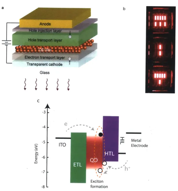
film, the electrons are impeded from further progress by an energy barrier from the hole transport layer. From the opposite side, holes are transported across a thin film of amorphous small organic molecules. Due to the larger hole injection barrier between the organic molecules and the QD film, holes accumulate on molecules next2.2. QUANTUM DOT LIGHT EMITTING DIODES a b
A
Transparent cathode Glass C LU -3 -4 -5 -6 -7 -8 h.e
ITO I Metal Electrode Exciton formationFigure 2-2: (a) Illustration of a hybrid organic-inorganic QD-LED (b) Photograph
of QD-LEDs used in this thesis (c) Energy band diagram of a typical hybrid QD-LED.
CHAPTER 2. COLLOIDAL QUANTUM DOTS AND LIGHT EMITTING DIODES
to the QD film. Because of this band alignment, excitons are on QDs at the interface with the hole transport layer. A schematic illustration of this structure is shown in Figure 2-2.
Using this structure, peak external quantum efficiencies of >20% have been achieved for red, green and blue devices. These efficiencies have reached the outcoupling limited ceiling of 20-25%, and approaches those of commercial phosphorescent OLEDs. The
brightness of these devices have also reached record levels of 460000cdm 2 [LZF+ 18].
Further improvements towards commercialization will require the full combination of high brightness, high efficiency, and long device operating lifespan.
2.2.2
Efficiency Loss Mechanisms
The external quantum efficiency ?7EQE of a QD-LED is defined as the ratio of the
number of photons emitted to the number of electrons injected. It can be can be
separated into the internal quantum efficiency TIQE and the out-coupling efficiency
r0C. That is,
?7EQE =
?7IQEr)0C-The out-coupling efficiency is the fraction of photons emitted that radiate into free space through the transparent substrate. For a planar device with a metallic electrode and glass substrate, Roc ~ 20%. The remaining photons either couple into waveguided modes or plasmonic modes of the electrode. Various approaches to
improving rboc include controlling the emitter dipole orientation [SKK+18],
textur-ing the transparent substrate or incorporattextur-ing microlens arrays [LHL+08], and ustextur-ing metallic nanostructures to modify the local density of states of the emitters [LRVG16].
These approaches can increase out-coupling efficiency to roc > 70%. In this thesis,
we only focus on the internal efficiency loss mechanisms and therefore do not employ these strategies. We simply position the QD film at a position with maximum optical 32
field intensity (near A/4 from the metal electrode), thereby obtaining rboc ~ 20%. The internal quantum efficiency can be further written as rIQE = 7rPL, where
97 is the fraction of injected charges that eventually recombine (rather than exiting
the device from the opposite electrode) and TPL is the average PLQY of the excitons that are formed. In the hybrid organic-inorganic QD-LED structure in Fig. 2-2, both electron and holes can be confined on the QD film by an energy barrier of > 1.5eV from the adjacent transport layers, and therefore leakage current is also typically small.
Therefore, the most significant efficiency loss mechanism in a QD-LED is due to rqPL. Even though near-unity solution PLQY QDs can be readily synthesized by carefully passivating defect states, there are still myriad of factors that can reduce TPL of a QD within a solid-state film in an operating LED. Here, we give a brief overview of these factors:
1. A large electric field can reduce the electron-hole wavefunction overlap of an
exciton, thereby decreasing the radiative recombination rate.
2. A large electric field can increase the coupling between delocalized carriers and localized defect states by changing the relative energies of these states. The defect states then act as intermediate centers for non-radiative recombination.
3. Excess charge accumulation can lead to the formation of charged excitons, which
typically have low PLQY due to non-radiative Auger recombination.
4. Joule heating can lead to the reduction of PLQY by changing the electron-phonon coupling strength, thereby modifying trapping rates of delocalized car-riers.
5. Energy transfer via FRET can funnel excitons to dark sites, which lowers the QD film PLQY relative to solution PLQY.
CHAPTER 2. COLLOIDAL QUANTUM DOTS AND LIGHT EMITTING DIODES (b) (c) ~~0~ (e) ~0~ ~0~ Cf)
Figure 2-3: Schematic illustrations of different loss mechanisms
Reduction of electron-hole wavefunction overlap in an electric field non-radiative recombination (c) Auger recombination (d) Joule coupling to defect states (e) Energy transfer to "dark" QDs (f) the electron transport layer.
ETL
in a QD-LED. (a)
(b) Defect assisted
heating enhanced Charge-transfer to
6. Charge transfer to mid-gap defect states in the metal oxide electron transport
layer can quench QD photoluminescence.
Detailed analysis of many of the above mechanisms will be provided in the rest of the thesis.
(a)
(d)
34
Chapter 3
Direct Measurement of Charge and
Electric Field in a Quantum Dot
Light Emitting Diode
Most of the existing experimental methods to probe the device physics in QD-LEDs involve an iterative process of modifying device structure or material set and observ-ing the effects in terms of the electroluminescence spectra, current-voltage curves, and luminescence efficiency. While this approach has lead to the identification of efficiency loss mechanisms and provided useful engineering guidelines, quantitative understand-ing of basic device physics remain scarce. Because the efficiency of a device results from the complex interplay between charge and electric field in each of the multiple transport/emissive layers and interfaces between them, even the modification of a single component in the system can lead to unexpected effects. Therefore, in order to obtain a unambiguous picture of QD-LED operational behavior, it is imperative to be able to directly measure internal variables such as charge and electric field of a device in operation.
CHAPTER 3. DIRECT MEASUREMENT OF CHARGE AND FIELD IN A QD-LED
electroluminescence (EL) efficiency and an unbalanced injection of electrons and holes into the QDs that result in non-radiative Auger recombination [BPL+13, SSDD18]. Other studies have demonstrated that a large electric field can reduce the spatial overlap of electron and hole wavefunctions, thereby lowering the rate of radiative re-combination [BYW13, SSTB13]. However, the deleterious nature of these two effects has neither been disentangled nor quantified. Moreover, a systematic understanding of how physical parameters such as charge carrier mobility and interfacial hopping rates govern charge and field distribution in a device is also highly desirable for ra-tional optimization of device efficiency.
3.1
Survey of Optical Characterization Techniques
Due to the requirement of in situ characterization, we are limited to using non-invasive optical methods. At the simplest level, EL and PL spectra of an operating
QD-LED can be used to deduce its internal state [BPL+13]. However, QD-LEDs
produce narrow spectra that shift or broaden by at most a few nm through the entire range of device operation. Given the multitude of physical effects that influence the spectral shift or broadening, including electric field, free charge carrier accumulation, temperature, charge trapping, and changes in emission zone, it is nearly impossible to say anything quantitative about any of these quantities. Time-revolved PL can help differentiate some of the effects, but it can be only used at very low bias when the EL does not overwhelm the PL [BPL+13, SSDD18].
Beyond these methods, a number of linear and nonlinear optical techniques have been developed for OLEDs in the past two decade. Linear optical techniques can all be broadly referred to as electro-modulation spectroscopy, where bias to the de-vice is modulated and the change in amplitude of an optical probe beam is detected via a lock-in method. This class of techniques include electroabsorption spectroscopy, which detects change in absorption spectrum due to the Stark effect caused by an
A
3.1. SURVEY OF OPTICAL CHARACTERIZATION TECHNIQUES 37
tric field [CJP95], and charge modulation spectroscopy, which measures the magni-tude of an induced near-infrared absorption band from charged molecules [MHYR14]. Nonlinear techniques rely on electric field induced changes in the nonlinear optical properties of a molecular film. For example, optical polarization of an intense laser pulse at the second harmonic can be written as
p2w = X E E + x E Ew Ef, (3.1)
where EO is the static electric field, E' is the optical field, and X and X are second and third order non-linear susceptibility tensors respectively. Changes in the efficiency of second harmonic generation can therefore be linked to a local static electric field. This is known as the electric-field induced second harmonic generation
(EFISHG) method [MI16].
Unfortunately, direct application of established techniques to QD-LEDs is chal-lenging. First of all, charge carrier trapping in a QD film leads to hysteretic behavior with respect to applied bias on a time scale ranging from milliseconds to hours, which makes electro-modulation signals frequency dependent and muddles the interpreta-tion. A further complication arise from the large physical size of nanocrystals as com-pared to molecules. For an OLED, only a minute fraction of molecules are charged during operation, so that the strength of the charge-induced absorption bleach signal is far weaker than the field-induced Stark shift of the absorption spectrum, which contain contributions from every single molecule in the film. On the other hand, the volume of a single nanocrystal (- 1000nm3) is equivalent to a volume containing
> 1000 molecules. A much larger fraction of QDs in the film become charged during
operation, which makes charge and field induced changes in absorption spectra of similar magnitude, thereby complicating the analysis. Nonlinear optical methods are equally difficult to apply to QD-LEDs. Again, hysteresis limits the rate at which signals from repeated optical pulses could be averaged to achieve sufficient
signal-to-CHAPTER 3. DIRECT MEASUREMENT OF CHARGE AND FIELD IN A QD-LED
noise ratio. The non-linear response also depends on both the bulk and surface of the nanocrystals [JBOO], making it difficult to analyze the result.
3.2
Our Approach
To overcome these difficulties, we present a method that we refer to as differential absorption spectroscopy to directly measure charge accumulation and electric field in the QD film in operating QD-LEDs. Differing from electro-modulated techniques, device bias is held constant during the acquisition of an absorption spectrum using a widely-tunable visible laser source. The method does not rely on electrical modulation and is thus applicable to devices exhibiting hysteresis. We use balanced detection to removed laser noise and low-frequency drift, which are general challenges to DC laser absorption measurements. A global fitting method is used to simultaneously extract charge density and electric field. By studying a series of devices with different QD film thickness, we develop a quantitative electrostatic model of charge transport that explains current-voltage characteristics of a device. This technique can be combined with simultaneous measurement of EL spectra, PL spectra, and time-resolved photo-luminescence (TRPL) to decouple the influence of charge and field on EL efficiency. Specifically, by comparing the EQE of a QD-LED to varying electron accumulation at the same electric field, we find that charge occupation statistics, in addition to total charge accumulation, is an important factor. Finally, analyzing the correlation between electron accumulation and PL quenching of the QD film under bias gives the surprising result that the PLQY of charged nanocrystals can actually improve under a large electric field.
3.2. OUR APPROACH 39 a b -3 Alk C0 CBP k -4 -2) c-6-Lu -7 -8 ITO 0K Al0 C d E 1 0 0.8 0.6 .E 0.4 00.2 LuJ 550 6 )0 650 700 750 800 Wavelength (nm)
Figure 3-1: (a) Cross-sectional TEM image of an QD-LED with a single monolayer
QD film (b) Energy band diagram of an QD-LED (c) Normalized photoluminescence
(PL) spectrum of an QD film inside an QD-LED at OV bias (blue) and normalized electroluminescence (EL) spectrum of the same device at 4V bias (red). (Inset: pho-tograph of an operating QD-LED showing uniform illumination). (d) Optical char-acterization setup that measures differential absorption spectrum, EL/PL spectrum, and time-resolved PL. to spectrometer 405nm laser balanced BS M001i PD BS spatial filter bias v QD-LED SuperK 3.2. OUR APPROACH 39 I 0
CHAPTER 3. DIRECT MEASUREMENT OF CHARGE AND FIELD IN A QD-LED
3.3
Device Structure and Measured Quantities
To begin, we fabricate a series of QD-LEDs with the inverted structure using col-loidally synthesized CdSe/ZnCdS core-shell QDs with peak emission at 625 nm [Fig. 3-1(c)]. Each device comprises an inorganic electron transport layer (ETL) and an organic hole transport layer (HTL) sandwiching one to two monolayers of emissive QDs (Fig. 3-1(a, b)). Under positive bias, electrons are injected into the QD film due to good conduction band (CB) alignment between ZnO and QDs. For devices with multiple monolayers of QDs, electrons then drift toward the QD/HTL interface where they accumulate due to the shallow lowest unoccupied molecular orbital (LUMO) of the HTL. Holes are injected from the Al anode and gather at the QD/HTL interface as a result of an - 0.5 eV energetic barrier between the highest occupied molecular
orbital (HOMO) of the HTL and the valence band (VB) of the QDs. An electric field assists the holes across this barrier to form excitons on the QD film, which recombine to yield photons. The absolute PLQY of an QD film on glass is measured to be 75% in an integrating sphere using the method of de Mello [dMWF97]. The high PLQY not only enables a peak device EQE of 14% but also simplifies the analysis of effi-ciency loss mechanisms by limiting the contribution of intrinsic non-radiative decay pathways. Four QD-LEDs with QD film thicknesses of 10nm, 12nm, 18nm, and 23nm are used in this study, which we refer to as D1 to D4 herein.
Studies [BPL 13, SSDD18] have qualitatively shown that this structure is prone to an oversupply of electrons due to facile electron injection and slow hole injec-tion, which enhances the probability of forming negatively charged excitons (X-) that exhibit significantly lower PLQY compared to neutral excitons (X0). The spa-tial distribution of electrons on the QD film is non-uniform, as an electric field of
1 - 2MV/cm, constituting an energy difference of > 1 V between neighboring QD
monolayers, drives all electrons to reside on the monolayer closest to the HTL. We therefore describe QD charging in terms of the mean number of electrons per QD 40
on this final monolayer, denoted by (Ne), which is divided into those occupying ISe states or localized defect states, denoted by (Nls) and (N,"C) respectively [Fig.
3-1(b)]. To precisely define the spatial extent of the above averaging and what is meant by "one monolayer" is tricky because our QDs do not form perfect integer number
of closed-packed monolayers when spun-cast on ZnO; in fact, the exact quantity of interest is not well-defined since the organic molecules of the HTL can penetrate into the gaps between QDs at the surface of the film and come into contact with the QDs underneath [PanlO]. We therefore use the working definition that "one monolayer" contains a density of QDs corresponding to the film in Dl, which is the thinnest possible in our QD-LEDs without noticeable leakage current under forward bias and is measured to have a thickness equivalent to one QD diameter by ellipsometry.
In the following sections, we embark to measure these quantities through three experiments. 1) Using differential absorption spectroscopy we extract a quantity proportional to (ANs(V)), the number of 1Se electrons per QD injected under bias
V, compared with zero bias; 2) the proportionality factor and (AN,"c(V)) is evaluated
using a capacitor structure, and 3) the mean iSe occupation per QD under OV bias, denoted by (Nis), is determined by TRPL. Together we have
(NeS(V)) = (Ns) + (ANis(V)) (3.2)
The absence of electrons in the bulk of the QD film due to the driving field means that most of the QDs experience the same field strength, which we denote by EQD and directly extract from the differential absorption spectra. Quantitative knowledge of both charge density and the electric field then allows us to construct a simple model of charge transport.
CHAPTER 3. DIRECT MEASUREMENT OF CHARGE AND FIELD IN A QD-LED b 10 5 0 -5' 500 5 WC V increasing re;s is 500 550 600 650 700 Wavelength (nm) 0.12 2S . 0.1 0.08 0.06 s 0.04 .0 1/2 2S1/2 0.02 3S12 50 600 650 700 velength (nm) 10 8 6 4 2 0 -2 x10⁻³
increasing forward bias
500 550 600 650 70 Wavelength (nm) 0 f 6 -3 4 0 -2 --- tRew Spectrum Fited Spctrum . --- Bleach Spectrum - Stark Spectrum 550 600 650 Wavelength (nm) 700
Figure 3-2: (a) Capacitance structure for calibrating the magnitude of the
differ-ential absorption spectra to 1Se electron occupation. (b) Representative differdiffer-ential absorption spectrum (blue) measured in the capacitor structure at 12V. For compar-ison is the linear absorption spectrum of an QD film on glass (solid red) as well as
its second derivative (dotted red). (c) Transitions bleached by ISe filling. (d)
Dif-ferential absorption spectra of a QD-LED under reverse bias of -4V to -20 V. (e) Differential absorption spectra of a representative QD-LED under forward bias. (f)
Decomposing a typical QD-LED differential absorption spectrum into an iSe bleach
spectrum and a Stark spectrum.
a d 10 5 0 -5 42 is 3Qi-. 2S 1ns-. -... -.... -.