HAL Id: hal-01900789
https://hal.archives-ouvertes.fr/hal-01900789
Submitted on 15 Mar 2019
HAL is a multi-disciplinary open access
archive for the deposit and dissemination of
sci-entific research documents, whether they are
pub-lished or not. The documents may come from
teaching and research institutions in France or
abroad, or from public or private research centers.
L’archive ouverte pluridisciplinaire HAL, est
destinée au dépôt et à la diffusion de documents
scientifiques de niveau recherche, publiés ou non,
émanant des établissements d’enseignement et de
recherche français ou étrangers, des laboratoires
publics ou privés.
Quantitative correlation between Flash and equivalent
transistor for endurance electrical parameters extraction
V. Della Marca, J. Postel-Pellerin, T. Kempf, A. Regnier, P. Chiquet, Marc
Bocquet
To cite this version:
V. Della Marca, J. Postel-Pellerin, T. Kempf, A. Regnier, P. Chiquet, et al.. Quantitative correlation
between Flash and equivalent transistor for endurance electrical parameters extraction.
Microelectron-ics Reliability, Elsevier, 2018, 88-90, pp.159 - 163. �10.1016/j.microrel.2018.06.116�. �hal-01900789�
Quantitative correlation between Flash and equivalent transistor
for endurance electrical parameters extraction
V. Della Marcaa,*, J. Postel-Pellerina, T. Kempfabc, A. Regnierb, P. Chiqueta, M. Bocqueta a Aix-Marseille Université, IM2NP, CNRS, UMR 7334, 13397 Marseille, France b STMicroelectronics, Rousset, France
c Polytech’Lab / Nice Sophia-Antipolis University, Biot, France
*Corresponding author, Tel.: +33(0)413554037; E-mail address: [email protected] Abstract
Nowadays, the study of physical mechanisms that occur during Flash memory cell life is mandatory when reaching the 40nm and beyond nodes in terms of reliability. In this paper we carry out a complete experimental method to extract the floating gate potential evolution during the cell aging. The dynamic current consumption during a Channel Hot Electron operation for a NOR Flash is a proper quantitative marker of the cell degradation. Here both drain and bulk currents are measured and monitored throughout the endurance tests. We coupled these characteristics with quasi-static measurements to correlate the cell degradation with an equivalent transistor. The final goal is to be able to split the physical effects of repetitive hot carrier and Fowler-Nordheim operations, typical of Flash memories, to extract the electrical parameters evolution on a simple equivalent transistor.
Keywords: Floating Gate, charge trapping, endurance degradation, equivalent transistor, NVM. 1. Introduction
In the semiconductor non-volatile memories world, we observe an increasing production of resistive switching devices [1-4], even if the floating gate Flash still share a large percentage of the market. The charge storage devices, for embedded applications, are today scaled toward the 40nm node and beyond [5-7]. The Flash programming scheme has been adapted to satisfy the new constraints imposed by the smart connected object application field, to remain competitive with respect to the new devices, very aggressive in terms of energy consumption and scaling [8, 9]. Last but not least, the cell architecture has been modified in a 2T memory and split gate (1.5T) [10-12] or even, using a FD-SOI technology [13]. This kind of improvements can decrease the cell energy consumption and leakages, in order to address the ultra-low power applications. One of the main issue in these new architectures is the coupling factor estimation to evaluate the Flash programming efficiency [14-17]. It is very complicated today to compute the effect of parasitic capacitances once the single cell is arranged in an array. In this paper we propose to adapt the experimental technique presented in [18] to the standard Flash processed by STMicroelectronics. In the first part we describe the measurement setup used for the electrical characterizations and endurance tests on the standard cell and its equivalent transistor. Thus, we show the importance to consider the dynamic source current during a Channel Hot Electron (CHE) operation, to find the real cell coupling factor. In this way it is possible to extract the real floating gate potential (VFG) variation during the programming time (tP), as qualitatively proposed in [19]. Moreover, in the second section, a smart test algorithm is presented to induce a quantitative degradation on the equivalent transistor corresponding to the memory cell during cycling. The dynamic current consumption will be used as a marker of tunnel oxide degradation for both devices. Thanks to the four fully arbitrary pulse generators, the floating gate potential will be adjusted during cycling. Hence, the drain and bulk current contributions are needed to understand the charge trapping localization. This technique can be useful to characterize equivalent transistor during the
parametric test phase, after wafer fabrication to quickly get the cell degradation information. In fact, the future aim is to correlate these results, that has a duration of several minutes, with DC stress measurements and find a way to get the outcome in a shorter time. Moreover, it will be possible to characterize the tunnel oxide using other techniques like charge pumping to make sure that the corresponding oxide degradation is applied. Finally, we will demonstrate the validity of our method, and we show the dynamic characteristics degradation not only in terms of source current but also as a contribution of bulk current that represents here 15% of the global consumption and cannot be
neglected. We compare the results of adaptive cycling with the non-adaptive experiment to validate our
evaluation of real cell degradation on an equivalent transistor for quantitative parameters analysis which cannot be directly performed on the memory cell.
2. Experimental details
2.1. Samples and measurement setup
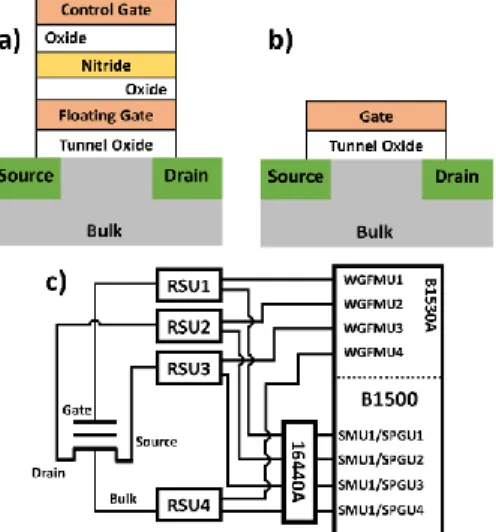
In this work the samples are taken from standard single Flash floating gate memory cells and the related equivalent transistors (dummy cells) are implemented on 200mm wafers. The cell dimensions are 0.07μm in width and 0.16μm in length. The tunnel oxide is a standard thermally grown SiO2 while the interpoly-dielectric is an
Oxide/Nitride/Oxide (ONO) tri-layer stack (Fig. 1a). The equivalent transistor has the same size, with the possibility to directly bias the floating gate (Fig.1b). A complete set of electrical characterizations have been carried out during the endurance test using the experimental setup shown in Fig. 1c. The block diagram represents the Keysight B1500 equipped with 4 WGFMUs (Waveform Generator Fast Measurement Unit, Keysight B1530A), 4 SPGUs
(Semiconductor Pulse Generator Unit) and 4 SMUs (Source Monitor Unit). The switching between SMUs and SPGUs made with the 16440A selector, limiting parasitic elements. We connected in series the RSU (Remote-sense and Switch Unit) modules that enable the link with the probes and the DUT (Device Under Test). In the case of dynamic current measurements, they switch to WGFMU position enabling the fast pulse generation. In this last case the connection between the B1530 and the DUT is fully adapted to reduce the parasitic effect due to the connections. With this method we were able to perform quasi-static (DC) and dynamic measurements to obtain threshold voltage kinetics, pulsed current/voltage characteristics and current consumption plots.
Fig. 1. Block diagram of a) memory cell and b) equivalent transistor. c) Measurement setup. 2.2. Coupling factor extraction methodology
The coupling factor (αG) is the main parameter needed to apply a stress on dummy cell oxide equivalent to the stress of memory cell through cycling. Indeed, it is well known how to compute the floating gate potential as a function of the control gate voltage (VCG) during programming operation [17]. Nevertheless, the calculation of αG can be complicated because of parasitic capacitances due to the cell environment. Several techniques are available and explained in literature [14-17], but they combine quasi-static measurements on memory and dummy cells and thus a large dispersion is obtained due to variations in the fabrication process. Finally, we implemented the detailed technique in [18]. The source current consumption has been characterized for the memory (IS(tP)) using WGFMU (dynamic measurements) with a sampling time of 10ns. The source current versus gate voltage (IS(VG))
characteristics of the equivalent transistor at high drain voltage (VD=4.2V), were measured using a fast ramp (5μs) for the gate bias, to avoid the dummy cell tunnel oxide damage. In Fig.2a we reported a source current consumption of memory that is combined with an IS(VG) curve (Fig. 2b) to extract a quantitative evolution of floating gate potential during the CHE programming (VFG_PR). This last (Fig. 2c) is combined with the threshold voltage programming kinetic (VT_PR(t)), presented in Fig. 2d, to obtain the full experimental extraction of αG, as shown in Fig. 2e. The VT_PR corresponds to the VG applied on the control gate terminal to reach an IS current of 8µA when VD=0.7V.
Fig. 2. a) Measured source current consumption of memory cell. b) Measured source current versus fast ramped gate voltage of dummy cell. c) Extracted floating gate voltage during the programming operation. d) Measured memory programming threshold voltage kinetic. e) Floating gate voltage versus threshold voltage characteristic used for the coupling factor (αG) extraction.
3. Endurance on Flash and equivalent transistor
In this section, the endurance correlation between the memory device and the dummy cell is studied. 3.1. Dynamic current variation
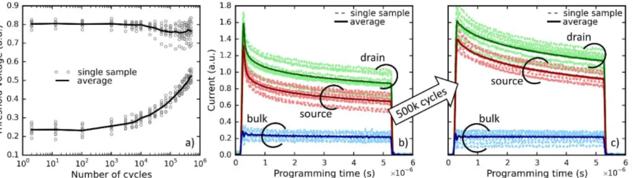
The floating gate memories are cycled up to 500k cycles with very stressful conditions, to highlight the parameters variations. For the CHE operation we used VCG=9V and VD=4.2V with tP=5μs, while the erase phase was performed using a 3ms square pulse (VCG=-16.5V). Moreover, for each cycling point shown in Fig. 3a (10 samples), we characterized the memory cell. In this way it will be possible to compute the VFG evolution during the cycling, to induce the same degradation on the equivalent transistor. In Fig. 3b and Fig. 3c we present the trend of drain, source, and bulk currents (ID, IS, IB) throughout the cell aging. We show the average evolution and the dispersion of ten samples. One can notice that the average bulk current slightly decreases after cycling stress while Is and Id increase is measured. This is due to the hot carrier degradation at the interface between the memory channel and the tunnel oxide. The drain and source current variation depends on the parasitic charge trapping close to the drain region [20], while the variation of bulk current indicates the tunnel oxide degradation in the middle channel region. The cell consumption is thus an indicator of endurance stress and can be used to refer to the tunnel oxide degradation of equivalent transistor.
Fig. 3. a) Endurance characteristics of 10 memory cells. Corresponding current consumption b) before and c) after 500k cycles (the average is highlighted).
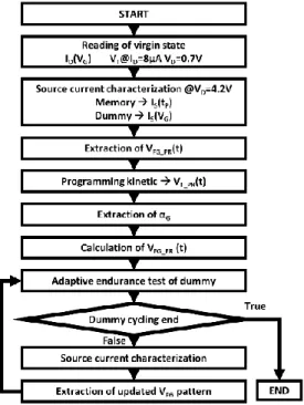
3.2. Adaptive cycling on dummy cell
In Fig. 4 we propose a smart algorithm used to generate the pulses for an equivalent transistor stress. After the initialization phase, reported in section 2.2, the dummy cell is cycled while the applied pulses on the gate terminal are adapted by using the parameters evolution of the memory cell. The new characteristics of the equivalent transistor are carried out during the dummy cycling test. Thanks to the wide panel of electrical characterizations carried out on memory and equivalent transistor, we can accurately compute the evolution of the floating gate potential.
The VFG_PR (Fig. 5a) is extracted from the measurements, as well as the coupling factor (αG), while the floating gate potential during the erase operation (VFG_ER) is computed applying the well-known formula presented in [17]. The results are reported in Fig. 5b. At the beginning of cycling we used the method presented in section 2.1 for the αG extraction. This coupling factor is kept constant during the endurance test and is used with the source current characteristics (Fig. 3) to calculate each time the updated VFG pattern to apply. It shows the importance to use the adaptive technique to emulate the degradation of tunnel oxide accurately. The parasitic charge trapping increases with the cell aging and this implies an alteration of electric field in the tunnel oxide that corresponds to an increase in the floating gate potential. It is interesting also to notice the changing of the VFG_PR shape with cycling that is linked to an increase of the cell current consumption Is(tP) (Fig. 3b and c).
Fig. 4. Flowchart of implemented smart algorithm for adaptive endurance test of dummy cell.
Fig. 5. Floating gate voltage a) extracted for the programming and b) computed for the erase operations, applied on dummy cell.
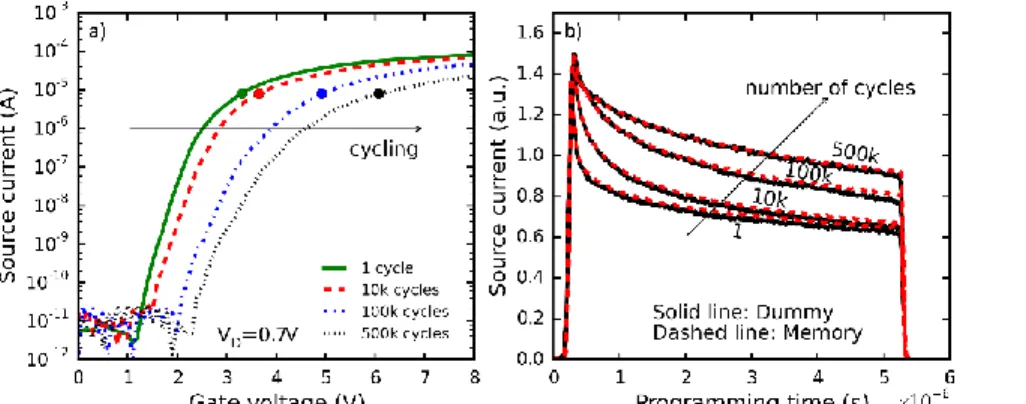
In Fig.6a a quantitative evolution of Is(VG) (VD=0.7V) dummy cell characteristics is thus representative of cell cycling degradation. The threshold voltage, the transconductance and the subthreshold slope can be extracted in order to show the charge trapping at the tunnel oxide/bulk interface. The points used to measure the threshold voltage evolution at IS=8µA are highlighted in Fig.6a. These characteristics are representative of the data presented in section 3.3 for the case of dummy cell cycling using an adaptive programming-erase pattern. The correlation between the extracted parameters on memory and dummy cell cannot ensure the good quantitative matching between the
degradation of both devices. Hence, we demonstrated the validity of our method using the dynamic source current as a marker of oxide degradation. Fig.6b shows Is(tP) before and after cycling test. This current is measured on the single cell applying VCG=9V and VD=4.2V (average source current from Fig.3b and c) and on the dummy cell using the extracted adaptive VFG from Fig. 5.
Fig. 6. a) Source current versus gate voltage reading characteristics of dummy cell during cycling. b) Source current during memory programming compared to the dynamic current of dummy cell measured applying the adaptive floating gate voltage.
The superposition of Is(tP) for both devices is the evidence of a good floating gate potential extraction. The source current that flows in the memory transistor channel depends on the floating gate potential [6, 17]. It indicates the programming efficiency loss and the charge trapping localization [20]. The current consumption monitoring is thus a marker of the memory cell degradation and it can easily be correlated with the tunnel oxide degradation of the equivalent transistor. Moreover, for low energy embedded applications this technique can be used to check the memory aging in order to improve the array reliability.
3.3. Discussion on equivalent transistor degradation
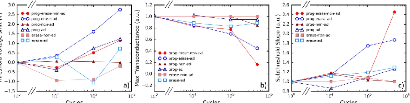
In this last section we present the evolution of the main electrical parameters of the equivalent transistor, under different stress conditions. In Fig. 7 we report respectively the threshold voltage shift (Fig. 7a), the maximum of transconductance (Fig. 7b) and the subthreshold slope variation (Fig. 7c). All these data are experimentally obtained applying the protocol presented in Fig.4 and varying the stress conditions. We cycled the dummy cell using either VFG_PR+VFG_ER complete pattern (prog-erase), only programming (prog) or only erasing (erase) VFG cumulative pulses. For these three stress schemes we applied both adaptive (ad) and non-adaptive (non-ad) algorithms to compare the experimental results. First, in Fig. 7a we show once again the importance of using the adaptive
technique to induce the real degradation on tunnel oxide. The threshold voltage shift in the case of prog-erase-non-ad VFG is underestimated. If we compare the erase threshold voltage evolution of memory cell in Fig. 3a with the results of Fig. 7a we can notice that the shift starts between 1k and 10k cycles as in the prog-erase-ad case. Moreover, stressing the dummy cell just with prog pulses, the threshold voltage variation disappears if a non-adaptive algorithm is used. Fig. 7b and Fig. 7c show the difference between unipolar stress (only prog or only erase) and bipolar stress. The highest stress is induced using the prog-erase cycling pattern. Once again, the difference between the two techniques is shown, revealing a larger degradation of electrical parameters in the case of adaptive cycling. Then, the highest variation is found in the last decade of endurance test.
Fig. 7. Evolution of main equivalent transistor parameters applying adaptive (ad) and non-adaptive (non-ad) stress conditions: a) threshold voltage shift, b) maximum of transconductance and c) subthreshold slope.
4. Conclusion
In this paper we used a fully experimental method to extract the coupling factor of an embedded Flash memory cell. By this way we computed the floating gate potential evolution during program/erase cycles. The aim was to be able to apply a quantitative adaptive gate potential on the equivalent transistor, in order to induce on the tunnel oxide the same endurance degradation as the memory cell. The main advantage of this technique is the possibility of using it for all charge storage device architectures: 1T, split gate, 2T with a select transistor. A complete set of dynamic and quasi-static (DC) electrical characterizations allowed us to obtain exhaustive results on the equivalent transistor. To demonstrate the reliability of our methodology, we used the dynamic source current as a marker of memory and dummy cell degradation. The electrical parameter extraction of dummy cell, using adaptive and non-adaptive stress, has shown the importance of implementing our smart algorithm to better understand the tunnel oxide degradation. This technique will improve the future characterizations of equivalent transistor to estimate quantitatively the degradation induced by hot carrier or Fowler-Nordheim stress. Moreover, it will be possible to combine this method to standard oxide characterizations like charge pumping or DC stress to make the manufacturing parametric test faster.
References
[1] C. C. Chou et al., "An N40 256K×44 embedded RRAM macro with SL-precharge SA and low-voltage current limiter to improve read and write performance," 2018 IEEE International Solid - State Circuits Conference - (ISSCC), San Francisco, CA, USA, 2018, pp. 478-480. doi: 10.1109/ISSCC.2018.8310392
[2] H. K. Yoo et al., "Engineering of ferroelectric switching speed in Si doped HfO2 for high-speed 1T-FERAM application," 2017 IEEE International Electron Devices Meeting (IEDM), San Francisco, CA, 2017, pp. 19.6.1-19.6.4. doi: 10.1109/IEDM.2017.8268424
[3] F. Pellizzer et al., "Novel μtrench phase-change memory cell for embedded and stand-alone non-volatile memory applications," Digest of Technical Papers. 2004 Symposium on VLSI Technology, 2004., 2004, pp. 18-19. doi: 10.1109/VLSIT.2004.1345368 [4] A. Belmonte et al., "Enhancement of CBRAM performance by controlled formation of a hourglass-shaped filament," 2017 17th
Non-Volatile Memory Technology Symposium (NVMTS), Aachen, 2017, pp. 1-5. doi: 10.1109/NVMTS.2017.8171281 [5] A. Dobri, S. Jeannot, F. Piazza, C. Jahan, J. Coignus, L. Perniola, F. Balestra, "Development and application of the Oxide Stress
Separation technique for the measurement of ONO leakage currents at low electric fields in 40nm floating gate embedded-flash memory," Microelectronics Reliability, Volume 69, 2017, Pages 47-51, doi.org/10.1016/j.microrel.2016.12.006.
[6] J. Coignus, G. Torrente, A. Vernhet, S. Renard, D. Roy and G. Reimbold, "Modelling of 1T-NOR flash operations for consumption optimization and reliability investigation," 2016 IEEE International Reliability Physics Symposium (IRPS), Pasadena, CA, 2016, pp. PR-1-1-PR-1-4. doi: 10.1109/IRPS.2016.7574630
[7] S. Tsuda et al., "Reliability and scalability of FinFET split-gate MONOS array with tight Vth distribution for 16/14nm-node embedded flash," 2017 IEEE International Electron Devices Meeting (IEDM), San Francisco, CA, 2017, pp. 19.3.1-19.3.4. doi: 10.1109/IEDM.2017.8268421
[8] C. Cagli et al., "Study of the Energy Consumption Optimization on RRAM Memory Array for SCM Applications," 2017 IEEE International Memory Workshop (IMW), Monterey, CA, 2017, pp. 1-4. doi: 10.1109/IMW.2017.7939106
[9] Y. K. Lee et al., "High-speed and logic-compatible split-gate embedded flash on 28-nm low-power HKMG logic process," 2017 Symposium on VLSI Technology, Kyoto, 2017, pp. T202-T203. doi: 10.23919/VLSIT.2017.7998171
[10] N. Do, "Scaling of split-gate flash memory and its adoption in modern embedded non-volatile applications," 2016 International Conference on IC Design and Technology (ICICDT), Ho Chi Minh City, 2016, pp. 1-4. doi: 10.1109/ICICDT.2016.7542072 [11] Y. Taito et al., "7.3 A 28nm embedded SG-MONOS flash macro for automotive achieving 200MHz read operation and
2.0MB/S write throughput at Ti, of 170°C," 2015 IEEE International Solid-State Circuits Conference - (ISSCC) Digest of Technical Papers, San Francisco, CA, 2015, pp. 1-3. doi: 10.1109/ISSCC.2015.7062961
[12] D. Shum et al., "Functionality Demonstration of a High-Density 1.1V Self-Aligned Split-Gate NVM Cell Embedded into LP 40 nm CMOS for Automotive and Smart Card Applications," 2015 IEEE International Memory Workshop (IMW), Monterey, CA, 2015, pp. 1-4. doi: 10.1109/IMW.2015.7150288
[13] J. M. Portal et al., "Design and Simulation of a 128 kb Embedded Nonvolatile Memory Based on a Hybrid RRAM (HfO2 )/28 nm FDSOI CMOS Technology," in IEEE Transactions on Nanotechnology, vol. 16, no. 4, pp. 677-686, July 2017. doi: 10.1109/TNANO.2017.2703985
[14] M. Wong, D. K. Y. Liu and S. S. W. Huang, "Analysis of the subthreshold slope and the linear transconductance techniques for the extraction of the capacitance coupling coefficients of floating-gate devices," in IEEE Electron Device Letters, vol. 13, no. 11, pp. 566-568, Nov. 1992. doi: 10.1109/55.192842
[15] B. Moison, C. Papadas, G. Ghibaudo, P. Mortini and G. Pananakakis, "New method for the extraction of the coupling ratios in FLOTOX EEPROM cells," in IEEE Transactions on Electron Devices, vol. 40, no. 10, pp. 1870-1872, Oct 1993. doi: 10.1109/16.277347
[16] K. Prall, W. I. Kinney and J. Macro, "Characterization and suppression of drain coupling in submicrometer EPROM cells," in IEEE Transactions on Electron Devices, vol. 34, no. 12, pp. 2463-2468, Dec 1987. doi: 10.1109/T-ED.1987.23336
[17] P. Pavan, R. Bez, P. Olivo and E. Zanoni, "Flash memory cells-an overview," in Proceedings of the IEEE, vol. 85, no. 8, pp. 1248-1271, Aug 1997. doi: 10.1109/5.622505
[18] W. L. Choi and D. M. Kim, "A new technique for measuring coupling coefficients and 3-D capacitance characterization of floating-gate devices," in IEEE Transactions on Electron Devices, vol. 41, no. 12, pp. 2337-2342, Dec 1994. doi: 10.1109/16.337446
[19] J. Coignus, A. Vernhet, G. Reimbold, G. Torrente, S. Renard and D. Roy, "Relaxation-free characterization of Flash programming dynamics along P-E cycling," 2015 IEEE International Integrated Reliability Workshop (IIRW), South Lake Tahoe, CA, 2015, pp. 119-121. doi: 10.1109/IIRW.2015.7437082
[20] V. Della Marca, J. Postel-Pellerin, G. Just, P. Canet and J.-L. Ogier, "Impact of endurance degradation on the programming efficiency and the energy consumption of NOR flash memories," Microelectronics Reliability, vol. 54, pp. 2262-2265, 2014.