HAL Id: hal-01578455
https://hal.archives-ouvertes.fr/hal-01578455
Submitted on 29 Aug 2017
HAL is a multi-disciplinary open access
archive for the deposit and dissemination of
sci-entific research documents, whether they are
pub-lished or not. The documents may come from
teaching and research institutions in France or
abroad, or from public or private research centers.
L’archive ouverte pluridisciplinaire HAL, est
destinée au dépôt et à la diffusion de documents
scientifiques de niveau recherche, publiés ou non,
émanant des établissements d’enseignement et de
recherche français ou étrangers, des laboratoires
publics ou privés.
Electronic properties of (Sb;Bi) 2 Te 3 colloidal
heterostructured nanoplates down to the single particle
level OPEN
Wasim Mir, Alexandre Assouline, Clément Livache, Bertille Martinez, Nicolas
Goubet, Xiang Zhen Xu, Gilles Patriarche, Sandrine Ithurria, Hervé Aubin,
Emmanuel Lhuillier
To cite this version:
Wasim Mir, Alexandre Assouline, Clément Livache, Bertille Martinez, Nicolas Goubet, et al..
Elec-tronic properties of (Sb;Bi) 2 Te 3 colloidal heterostructured nanoplates down to the single particle
level OPEN. Scientific Reports, Nature Publishing Group, 2017, 7, pp.9647 - 9647.
�10.1038/s41598-017-09903-w�. �hal-01578455�
www.nature.com/scientificreports
Electronic properties of (Sb;Bi)
2
Te
3
colloidal heterostructured
nanoplates down to the single
particle level
Wasim J. Mir
1,2, Alexandre Assouline
3, Clément Livache
1,3, Bertille Martinez
1, Nicolas
Goubet
1,3, Xiang Zhen Xu
3, Gilles Patriarche
4, Sandrine Ithurria
3, Hervé Aubin
3&
Emmanuel Lhuillier
1We investigate the potential use of colloidal nanoplates of Sb2Te3 by conducting transport on single
particle with in mind their potential use as 3D topological insulator material. We develop a synthetic procedure for the growth of plates with large lateral extension and probe their infrared optical and transport properties. These two properties are used as probe for the determination of the bulk carrier density and agree on a value in the 2–3 × 1019 cm−3 range. Such value is compatible with the metallic
side of the Mott criterion which is also confirmed by the weak thermal dependence of the conductance. By investigating the transport at the single particle level we demonstrate that the hole mobility in this system is around 40 cm2V−1s−1. For the bulk material mixing n-type Bi
2Te3 with the p-type
Sb2Te3 has been a successful way to control the carrier density. Here we apply this approach to the
case of colloidally obtained nanoplates by growing a core-shell heterostructure of Sb2Te3/Bi2Te3 and
demonstrates a reduction of the carrier density by a factor 2.5.
Bismuth and antimony chalcogenides (tetradymite group with formula such as (Sb;Bi)2(Se;Te)3) have attracted
great interest in the past for their thermoelectric properties1–5. The heavy mass of these materials leads to a large
spin orbit coupling which results in an inverted band structure. Over this past decade, it is the original electronic structure of bismuth and antimony chalcogenides which has driven most of interest in these compounds. Indeed they appear as model 3D topological insulator6–9, with conducting surface-states and an insulating core, as long
as the material can be obtained under an intrinsic form.
Sb2Te3 is a 0.3 eV band gap semiconductor. This material has common antisite defects10–12 where Sb atoms
replace Te atoms, which tends to result in a p-type doping13. Controlling the bulk carrier density in topological
insulator compounds is a key challenge since the Fermi level of the material needs to be close to its Dirac point for electronic transport to be dominated by topologically protected surface states. Moreover, the conductance of the material is the sum of the surface and bulk contribution. Because of the narrow band gap nature of these topolog-ical insulator materials and their deviation from stoichiometry, the bulk is generally not as insulating as desired. By reducing the bulk carrier density and the associated conductance, the weight of the surface contribution in transport is expected to increase and make the surface observation more likely to occur.
The Mott criterion can be used to estimate whether the material will behave as a metal or as an insulator. Metallic behavior is expected to occur if a n0 1/3> .0 2514, where n is the carrier density and =a πε ε⁎
h m e 0 r 2 0 2 the Bohr
radius with h the Planck constant, ε0 the vacuum permitivity, εr the material dielectric constant, m the effective ⁎
mass and e the proton charge. Due to large dielectric constant (ε > 50) of Sb2Te3, the Bohr radius is large which
1Sorbonne Universités, UPMC Univ. Paris 06, CNRS-UMR 7588, Institut des NanoSciences de Paris, 4 place Jussieu,
75005, Paris, France. 2Department of Chemistry, Indian Institute of Science Education and Research (IISER), Pune,
411008, India. 3Laboratoire de Physique et d’Étude des Matériaux, PSL Research University, CNRS UMR 8213,
Sorbonne Universités UPMC Univ Paris 06, ESPCI ParisTech, 10 rue Vauquelin, 75005, Paris, France. 4Laboratoire
de Photonique et de Nanostructures (CNRS- LPN), Route de Nozay, 91460, Marcoussis, France. Wasim J. Mir and Alexandre Assouline contributed equally to this work. Correspondence and requests for materials should be addressed to E.L. (email: [email protected])
Received: 9 May 2017 Accepted: 24 July 2017 Published: xx xx xxxx
www.nature.com/scientificreports/
makes the Mott criterion fulfilled even for low carrier densities. Typically the threshold carrier density is esti-mated to be ≈2 × 1016 cm−3 assuming an effective mass of 0.1 m
0 where mo is rest mass of an electron. As a result,
Sb2Te3 typically behaves as a metal6. Alloying n-type (Bi2Se3 and Bi2Te3) and p-type (Sb2Te3) materials is a possible
way to obtain a charge compensation and reduce the overall bulk carrier density. While this type of approaches have been extensively studied for bulk and thin film materials15–17 almost no work has been dedicated to
colloi-dally synthesized materials.
The tetradymites are layered 2D materials18, 19. Each layer is 1 nm thick and is composed of 5 atoms
(quintu-plet). So far, most of the efforts towards growth of these materials have been focused on physical methods such as molecular beam epitaxy20, chemical vapor deposition21, pulsed laser deposition and exfoliation22. Chemical
solvothermal methods have been proposed23, 24, however all these works were driven by the investigation of the
thermoelectric properties and very little work was dedicated to the understanding of the electronic and spectro-scopic properties of (Sb;Bi)2Te3 obtained under colloidal form. In this letter, we develop a colloidal synthesis of
Sb2Te3 nanoplates and investigate their transport properties from a thin film down to the single particle level. We
demonstrate that the material is indeed p-type. In the last part of the paper, we focus on the control of the carrier density within these plates by growing in solution a heterostructure combining an n-type (Bi based) and a p-type (Sb based) layer. We obtain by this way a decrease of the bulk carrier density by a factor ≈ 3. This work paves the way for the use of colloidal heterostructure as model 3D topological insulator.
Results and Discussion
Synthesis.
The chemical synthesis of Sb2Te3 nanoplates has been investigated using solvothermal methods inaqueous25–28, or polar organic solvents29–31. We see two main limitations to these approaches, which are (i) the risk
of oxidation of the material, and (ii) the final thickness of the nanoplate being limited to thick sheets (>50 nm26, 27).
Hot injection methods in organic solvents are well established and lead to high monodispersity. Synthesis of Sb2Te3 nanoparticles in organic medium has also been proposed32. The latter is based on the thermal
decomposi-tion of single precursor containing antimony and tellurium at high temperature33–35. In this report, we rather use
a bulky antimony precursor of antimony oleate, prepared from antimony acetate in presence of excess of oleic acid at a temperature where the acetic acid can be removed under vacuum (85 °C).
In a typical synthesis, the temperature is raised around 200 °C under Ar and the Te precursor (trioctylphos-phine complexed with Te) is quickly injected in the flask. The reaction is conducted in non-coordinating solvent such as octadecene since we observe that coordinating solvent such as oleylamine leads to the formation of oxide instead of the telluride. The solution rapidly darkens, and after 1 min a grey metallic appearance is observed. The product is cleaned via addition of polar solvent and by the help of centrifugation. The particles can be stored in non-polar solvents such as hexane and toluene, but typically an immediate precipitation of the suspension is observed. + ⟶ + ⟶ Sb OAc( ) OA C Sb OA( ) TOPTe Sb Te (1) vacuum C Ar 3 80 3 200 2 3
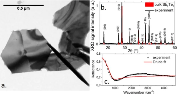
The obtained nanoplates typically present a hexagonal structure with lateral size ranging from 200 nm to 1 µm and a thickness from a few quintuplets (QL) up to 50 nm, see Figs 1a and S7. The detailed investigation of the effects of temperature, synthesis duration and stoichiometry on the final product is discussed in the SI, see Figs S1
to S5. The diffraction peaks from the XRD pattern are fully consistent with the trigonal phase (R 3 m) of Sb2Te3
Figure 1. (a) TEM image of Sb2Te3 nanoplates. (b) X-ray diffraction pattern for a film of Sb2Te3 compared with
www.nature.com/scientificreports/
(00-015-0874), see Fig. 1b. Energy dispersive X-ray (EDX) analysis (Fig. S6 and Table S1) confirmed the presence of both antimony and tellurium in the final compound and showed that the material is very close to stoichiometry Sb2Te3+x with x = −0.1 ± 0.05, but is systematically Te deficient, consistent with previous report of this
mate-rial10–12. This non stoichiometry of the compound is responsible for the metallic aspect of the solution and is
further confirmed by the reflectance measurement, see Fig. 1c. The IR spectrum in Fig. 1c is poorly structured which suggests that the absorption results from free electrons.
To confirm this hypothesis, we can model the reflectivity assuming a Drude model36, 37 for the free electrons.
In this case, the expression of the real ε( )1 and imaginary ε( )2 part of the dielectric constant are given by
ε ω ε ω ω γ = − + ∞ ( ) (2) p 1 2 2 2 and ε ω γω ω ω γ = + ( ) ( ) (3) p 2 2 2 2
where ε∞ is the dielectric constant at high frequency, ωp the plasmon frequency and γ the damping rate. The
reflectivity signal is given for a semi-infinite medium, by
ω = − + + + R n k n k ( ) ( 1) ( 1) (4) 2 2 2 2
with n and k respectively the real and imaginary part of the optical index. The latter can be related to the dielectric constant by ω = ε + ε +ε n( ) 2 (5) 1 12 22 and ω = ε +ε −ε . k( ) 2 (6) 12 22 1
We obtain a reasonable agreement with obtained experimental data, see Fig. 1c, assuming ω =2460cm−
p 1
and γ = fs1/ 14 . From the plasmon frequency, we can estimate the carrier density n from the equation
ω ε = ∞ ⁎ ne m (7) p 2
to be = . ×n 3 6 1019cm−3 which is consistent with the realization of the Mott criterion of metallic nature.
Transport in Sb
2Te
3nanoplates.
In the following section, we investigate the transport properties of thesingle Sb2Te3 nanoplate and correlate our observations with optical method of deducing the carrier density. We
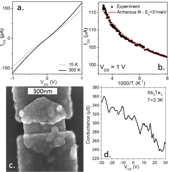
first start with ensemble measurements by conducting transport on nanoplates films. The films are conductive and present an ohmic behavior at room temperature, see Fig. 2a. The temperature dependence of the current pre-sents a small decrease of the conductance as the temperature is reduced, see Fig. 2b. between room temperature and 77 K, the temperature dependence is nicely fitted with the Arrhenius law, with a small activation energy of ≈30 meV. This is typical behaviour of thin films made of poorly coupled metallic grains38, 39.
Ultimately, the goal is to make single nanoparticle devices to observe the signature of surface states. In the next step, we switch from ensemble measurement to single particle measurement. Connecting a single nanocrystal can be especially difficult40–42, however the large lateral extension of the Sb
2Te3 nanoplate makes possible the
connec-tion of a single particle using careful e-beam lithography, see Fig. 2c.
After wire-bonding of the connections to the single nanoplate, the sample is immediately cooled down to low-temperature (2.3 K). The conductance at zero drain voltage is measured with a lock-in (IAC = 10 nA) as
func-tion of the gate voltage, Fig. 2d. We observe a p-type behavior with a rise of the conductance as holes (VGS < 0)
are injected in the nanoplate. The conductance as a function of gate voltage show reproducible fluctuations which are not simply due to electrical noise. These fluctuations are most likely related to Coulomb blockade or possi-bly universal conductance fluctuations41, 42. Indeed, while regular Coulomb peaks as a function of gate voltage
are usually observed in nano-sized devices weakly coupled to the electrodes, however, when the device is more strongly coupled to electrodes as in the measurement presented in this paper, the Coulomb peaks become fainter oscillations. Furthermore, because the conductance in a nanoplatelet is not averaged on a macroscopic number of disorder configurations, the conductance fluctuates with the gate voltage because of the changing electrostatic potential responsible for electron scattering.
www.nature.com/scientificreports/
= ∂ ∂ ∑ µ L WC V i V (8) DS GSwith L the inter electrode spacing (≈120 nm), W the width of the film (≈420 nm), C the sheet capacitance (11.5 ∑
nF.cm−2), V
DS the applied bias and ∂V∂i
GS the transconductance. We estimate the mobility in the single plane to be
in the 30–50 cm2V−1s−1 range which is only one decade below the typical values obtained for molecular beam
epitaxy (MBE) grown film43.
We can then use this mobility value to estimate the transport carrier density ntrans. The latter relates to the conductance (G) through the relation
= µ
n L
eWt G (9)
trans
where t is the nanoplate thickness (≈10 nm). We estimate the value to be 1.8 × 1019 cm−3 in good agreement with
our estimation based on optical measurements.
Control of carrier density.
Transport and optical measurement agree over a bulk hole carrier density in the 2–3 × 1019 cm−3 range. We can use this value to determine the position of the Fermi level with respect to the Diracpoint: −ED EF. The Fermi vector is estimated to be
Figure 2. (a) Current as a function of applied bias for a thin film of Sb2Te3 nanoplates. The measurement is
made in vacuum. (b) Current as a function of temperature for a thin film of Sb2Te3 nanoplates. (c) SEM image of
a single Sb2Te3 nanoplate connected to two Al electrodes. (d) Transfer curve (conductance as a function of gate
www.nature.com/scientificreports/
π
= = . −
kF (3 2 1/3n) 0 9nm 1 (10)
we can thus estimate
− = =
ED EF v kF F 295meV (11)
using vF the Fermi velocity7 taken as 5 × 10⁵ m.s−1. To reduce this energy shift between the Fermi level and the
Dirac point of this material we then investigate the mixing of the p-type Sb2Te3 nanoplate with n-type Bi2Te3
material. To do so, we conduct the same reaction as before and replace a part of the antimony oleate by bismuth oleate. The reaction leads to the formation of (Sb;Bi)2Te3 heterostructured nanoplates, see Fig. 3a–c. Their lateral
extension is reduced as the Bi content rises. Typically, 500 nm nanoplates are obtained for Sb rich material, while nanoplates with lateral extension below 200 nm are obtained with Bi rich condition. The lamellar aspect of the material is highlighted by conducting high resolution TEM on nanoplates lying on the side, see Fig. 3d.
We synthetize a series of (Sb;Bi)2Te3 nanoplates with various Bi content and then use the same fitting approach
as for the reflectance of the film of Sb2Te3 to determine for each Bi ratio the value of the plasma frequency and the
associated carrier density, see Figs 3e and S11, Table S3. As the Bi content is increased, we observe that the carrier density drops and passes by minimum around 30%. Here the carrier density is reduced by a factor 2.5 compared to pure Sb2Te3 nanoplates. The dependence of the carrier density with the Bi content is not simply a V shape curve
as it may have been expected while switching from a p-type to n-type material. This results because of combina-tion of carrier density change and effective mass change while estimating the carrier density from the plasmon frequency. We further confirm the reduction of the metallic character by measuring the transport properties of the film, see Fig. 3f,g. (Sb;Bi)2Te3 nanoplates present a stronger temperature dependence with a drop of the
con-ductance by a factor 10 between 300 K and 15 K, while the drop was only of 20% for pure Sb2Te3 nanoplates in the
same range of temperature. The high temperature activation energy extracted from the Arrhenius fit is typically twice larger and equal to 56 meV (compared to 30 meV for Sb2Te3).
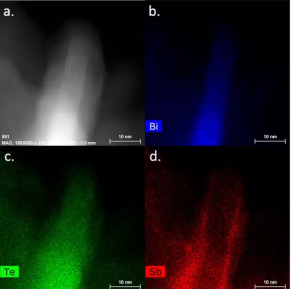
To unveil the exact nature of the formed (Sb;Bi)2Te3 nanoplates we use scanning transmission electron
micros-copy coupled with X-ray energy dispersive spectrosmicros-copy to combine nm scale resolution with chemistry com-position, see Figs 4, S12 and S13. The (Sb;Bi)2Te3 nanoplates are actually not forming an homogeneous alloy, but
rather from a core shell structure. The core is made of Bi2Te3, while the shell is made of Sb2Te3. This suggest a
higher reactivity of the bismuth compared to antimony towards tellurium, and is consistent with our observation that for similar growth conditions smaller nanoplates of Bi2Te3 are formed. Bi is more reactive towards Te which
favors the nucleation step and leads to the formation of lots of small seeds. Sb, which is less reactive than Bi will
Figure 3. TEM images of (a) Sb2Te3 nanoplates, (b) BiSbTe3 nanoplates, (c) Bi2Te3 nanoplates. (d) High
resolution TEM image of a Bi2Te3 nanoplate lying on the edge. (e) Optical carrier density as a function of
Bi content in (Sb;Bi)2Te3 heterostructure nanoplates. The error bars have been obtained by repeating the
measurement on several samples of a given composition. (f) Current as a function of temperature for a thin film of (Sb70;Bi30)2Te3 nanoplates. (g) Current as a function of applied bias for a thin film of (Sb70;Bi30)2Te3
www.nature.com/scientificreports/
react immediatelty with left over Te and grow a shell on the Bi2Te3 nanoplate, which behave as nucleation center.
The doping control which has been demonstrated here thus differs from the approach developed for bulk or thin film in this way that charge compensation occurs at the atomic scale in the heterostructure.
Conclusion
In this paper, we investigate the optical and transport properties of Sb2Te3 nanoplates with in mind their possible
use as nanosize topological insulator material. Both reflectance and transport measurement agree on the metallic character of these objects with a carrier density in the 2–3 × 1019 cm−3 range. We then demonstrate the feasibility
to conduct transport at the single particle level and determine the mobility to be between 30 and 50 cm2V−1s−1.
Finally we demonstrate that building an heterostructure of (Sb;Bi)2Te3 with a core shell structure can be reliably
used to tune the carrier density by a factor 2.5, down to the low 1019 cm−3 range.
Experimental Section
Chemicals.
Antimony acetate (Sb(OAc)3, 99.99% metal basis, Aldrich), bismuth acetate (Bi(OAc)3,99.999% metal basis, Aldrich), selenium powder (99.99% Strem Chemicals), tellurium powder (99.997% (trace metals basis), Alfa Aesar), Na2S nonahydrate (99,99%, Aldrich), Oleic acid (90% technical grade, Aldrich),
Trioctylphosphine (TOP 380, 98%, Cytec), octadecene (ODE, 90% technical grade, Aldrich), hexane (95% RPE-ACS, Carlo Erba), ethanol (anhydrous 99.9%, Carlo Erba), N-methyl formamide (NMFA, 99%, Alfa Aesar.)
Preparation of Sb(OA)
3.
In a 100 mL three neck flask, 1 g (3.35 mmol) of Sb(OAc)3 and 40 mL of oleic acidare loaded and put under vacuum at 85 °C for 30 min. The final solution is clear yellowish and used as a stock solution.
Figure 4. (a) HAADF STEM image of the (Bi,Sb)2Te3 nanoplate. The composition map of the Bi, Te and Sb of
www.nature.com/scientificreports/
Preparation of Bi(OA)
3.
In a 100 mL three neck flask, 0.5 g (1.3 mmol) of Bi(OAc)3 and 20 mL of oleic acidare loaded and put under vacuum at 85 °C for 30 min. The final mixture is used as a stock solution.
Preparation of 1 M TOPTe.
Trioctylphosphine complexed with tellurium is obtained by mixing 2.54 g of Te powder with 20 mL of TOP in a 50 mL three-neck flask. The solution is then degassed under vacuum for 30 min at 80 °C. The mixture is further heated under Ar at 270 °C until the powder gets fully dissolved. At this temperature the solution is orange and becomes yellow once cooled. The stock solution is kept in the glove box.Synthesis of Sb
2Te
3.
In a 25 mL three neck flask, 4 mL of the antimony oleate in ODE (0.33 mmol Sb) arediluted with 10 mL of additional ODE. The flask is degassed under vacuum at 85 °C for 30 min. Then the atmos-phere is switched to Ar and the temperature is raised to 200 °C. 0.5 mL of 1 M TOPTe is quickly injected and the solution rapidly turns metallic grey. The heating is continued for 5 min before the heating mantle is removed and air flow on the outside of the flask is used to cool the solution. The nanoparticles are precipitated by addition of ethanol and centrifuged for 3 min. The clear supernatant is discarded and the pellet is redispersed in hexane. The cleaning procedure is repeated two additional times.
Synthesis of Bi
2Te
3.
4 mL of the bismuth oleate solution (0.25 mmol Bi) and 10 mL of ODE are added to a25 mL 3 neck flask. The flask is degassed under vacuum at 85 °C for 30 min. The atmosphere is then switched to Ar and the temperature raised to 200 °C. 0.4 mL of TOPTe (1 M) are quickly injected and the solution rapidly turns metallic grey. The heating is continued for 5 min before the reaction is cooled down. The nanoparticles are precip-itated by addition of ethanol and centrifuged for 3 min. The cleaning procedure is repeated two additional times.
Material characterization.
Transmission electron microscopy (TEM) images were captured on JEOL 2010 and FEI Titan Themis microscopes. For X-ray diffraction (XRD), the nanoparticles were drop casted on a Si substrate from a hexane solution. Data was collected on a Philips X’Pert diffractometer equipped with Cu Kαline at 0.154 nm. Infrared spectra were measured on a Bruker Vertex 70 FTIR used in an ATR configuration with a ~700 °C globar source and a DTGS detector. The spectra were averaged 32 times with a resolution of 4 cm−1.
Energy dispersive X-ray analysis was conducted on an Oxford probe in a FEI Magellan scanning electron micro-scope at 10 kV and 100 pA.
Transport measurement.
For ensemble transport measurements, we prepared, using standard lithography methods, gold electrodes on Si/SiO2 wafers (400 nm of oxide). The electrodes are interdigitated and include 25pairs. Each electrodes is 2.5 mm long with a 20 µm spacing. Thin film of nanoplates over this interdigitated gold electrodes are subjected to ligand exchange with S2− ions by dipping the film of nanoplatelets within a solution
of Na2S in N-methylformamide44. The film is then rinsed in ethanol and dried. Measurements are made with a
Keithley 2400 source-meter, using a probe station operated in air at room temperature.
For single particle measurements, the solution of Sb2Te3 nanoparticle is first drop casted on a wafer. On this
wafer, the level of aggregation is high and prevents single particle connection. To obtain isolated single nano-plates, this film is transferred onto a Si/SiO2 wafer (300 nm of oxide) using a PDMS stamp. The film is then dipped
into a 1% Na2S in N-methyl formamide for 45 s. Two electrodes are deposited using standard e-beam approach.
Just before the metal deposition the surface is cleaned using Ar ion beam. Finally, 5 nm of titanium and 80 nm of aluminum are evaporated using an e-beam evaporator.
References
1. Poudel, B. et al. High-thermoelectric performance of nanostructured bismuth antimony telluride bulk alloys. Science 320, 634–638 (2008).
2. Talapin, D. V., Lee, J. S., Kovalenko, M. V. & Shevchenko, E. V. Prospects of colloidal nanocrystals for electronic and optoelectronic applications. Chem. Rev. 110, 389–458 (2010).
3. Venkatasubramanian, R., Colpitts, T., Watko, E., Lamvik, M. & El-Masry, N. MOCVD of Bi2Te3, Sb2Te3 and their superlattice structures for thin-film thermoelectric applications. J. Cryst. Growth 170, 817–821 (1997).
4. Jeon, H. W., Ha, H. P., Hyun, D. B. & Shim, J. D. Electrical and thermoelectrical properties of undoped Sb2Te3 and Bi2Te3-Sb2Te3-Sb2Se3 single crystals. J. Phys. Chem. Solids 52, 579–585 (1991).
5. Chatterjee, A. & Biswas, K. Solution-based synthesis of layered intergrowth compounds of the homologous PbmBi2nTe3n+m series as nanosheets. Angew. Chem. Int. Ed. 54, 5623 (2015).
6. Ando, Y. Topological Insulator Materials. J. Phys. Soc. Jpn. 82, 102001 (2013).
7. Zhang, H. et al. Topological insulators in Bi2Se3, Bi2Te3 and Sb2Te3 with a single Dirac cone on the surface. Nat. Phys 5, 438 (2009). 8. Hasan, M. Z. & Kane, C. L. Topological insulators. Rev. Mod. Phys. 82, 3045–3067 (2010).
9. Wei, Z., Rui, Y., Hai-Jun, Z., Xi, D. & Zhong, F. First-principles studies of the three-dimensional strong topological insulators Bi2Te3, Bi2Se3 and Sb2Te3. New J. Phys. 12, 065013 (2010).
10. Miller, G. R. & Li, C. Y. Evidence for the existence of antistructure defects in bismuth telluride by density measurements. J. Phys.
Chem. Solids 26, 173 (1965).
11. Horak, J., Cermak, K. & Koudelka, L. Energy formation of antisite defects in doped Sb2Te3 and Bi2Te3 crystals. J. Phys. Chem. Solids
47, 805 (1986).
12. Drasar, C., Lostak, P. & Uher, C. Doping and defect structure of tetradymite-type crystals. J. Electron. Mater. 39, 2162 (2010). 13. Horak, J., Drasar, C., Novotny, R., Karamazov, S. & Lostak, P. Non-stoichiometry of the crystal lattice of antimony telluride. Phys.
Status Solidi A 149, 549 (1995).
14. Mott, N. F. Metal-insulator transition. Rev. Mod. Phys. 40, 677–683 (1968).
15. Yang, F. et al. Top gating of epitaxial (Bi1-xSbx)2Te3 topological insulator thin films. Appl. Phys. Lett. 104, 161614 (2014). 16. He, X. et al. Highly tunable electron transport in epitaxial topological insulator (Bi1- xSbx)2Te3 thin films. Appl. Phys. Lett. 101,
123111 (2012).
17. Hong, S. S., Cha, J. J., Kong, D. & Cui, Y. Ultra-low carrier concentration and surface-dominant transport in antimony-doped Bi2Se3
topological insulator nanoribbons. Nat. Commun. 3, 757 (2012).
18. Nasilowski, M., Mahler, B., Lhuillier, E., Ithurria, S. & Dubertret, B. Two-dimensional colloidal nanocrystals. Chem. Rev. 116, 10934–10982 (2016).
www.nature.com/scientificreports/
19. Saha, S., Banik, A. & Biswas, K. Few-layer nanosheets of n-Type SnSe2. Chem. Eur. J. 22, 15634–15638 (2016).
20. Vidal, F. et al. Photon energy dependence of circular dichroism in angle-resolved photoemission spectroscopy of Bi2Se3 Dirac states.
Phys. Rev. B 88, 241410 (2013).
21. Lee, J., Brittman, S., Yu, D. & Park, H. Vapor-liquid-solid and vapor-solid growth of phase-change Sb2Te3 nanowires and Sb2Te3/ GeTe nanowire heterostructures. J. Am. Chem. Soc. 130, 6252–6258 (2008).
22. Teweldebrhan, D., Goyal, V. & Balandin, A. A. Exfoliation and characterization of bismuth telluride atomic quintuples and quasi-two-dimensional crystals. Nano Lett. 10, 1209–1218 (2010).
23. Konstantatos, G., Levina, L., Tang, J. & Sargent, E. H. Sensitive solution-processed Bi2S3 nanocrystalline photodetectors. Nano Lett.
8, 4002 (2008).
24. Scheele, M. et al. Synthesis and thermoelectric characterization of Bi2Te3 nanoparticles. Adv. Funct. Mater. 19, 3476 (2009). 25. Wang, W., Poudel, B., Yang, J., Wang, D. Z. & Ren, Z. F. High-yield synthesis of single-crystalline antimony telluride hexagonal
nanoplates using a solvothermal approach. J. Am. Chem. Soc. 127, 13792–13793 (2005).
26. Shi, W., Zhou, L., Song, S., Yang, J. & Zhang, H. Hydrothermal synthesis and thermoelectric transport properties of impurity-free antimony telluride hexagonal nanoplates. Adv. Mater. 20, 1892 (2008).
27. Shi, W., Yu, J., Wang, H. & Zhang, H. Hydrothermal synthesis of single-crystalline antimony telluride nanobelts. J. Am. Chem. Soc.
128, 16490–16491 (2006).
28. Zhou, N. et al. Size-controlled synthesis and transport properties of Sb2Te3 nanoplates. RSC Adv 4, 2427 (2014).
29. Zhou, B., Ji, Y., Yang, Y., F. Li, X. & H. Zhu, J. J. Rapid microwave-assisted synthesis of single-crystalline Sb2Te3 hexagonal nanoplates. Cryst. Growth Des. 8, 4394–4397 (2008).
30. Yang, H. Q. et al. Facile surfactant-assisted reflux method for the synthesis of single-crystalline Sb2Te3 nanostructures with enhanced thermoelectric performance. ACS Appl. Mater. Interfaces 7, 14263–14271 (2015).
31. Fei, F. et al. Solvothermal synthesis of lateral heterojunction Sb2Te3/Bi2Te3 nanoplates. Nano Lett. 15, 5905–5911 (2015). 32. Zhao, Y. & Burda, C. Chemical synthesis of Bi(0.5)Sb(1.5)Te3 nanocrystals and their surface oxidation properties. ACS Appl. Mater.
Interfaces 1, 1259–1263 (2009).
33. Gupta, G. & Kim, J. Facile synthesis of hexagonal Sb2Te3 nanoplates using Ph2SbTeR (R = Et, Ph) single source precursors. Dalton
Trans. 42, 8209 (2013).
34. Garje, S. S. et al. A new route to antimony telluride nanoplates from a single-source precursor. J. Am. Chem. Soc. 128, 3120–3121 (2006). 35. Schulz, S. et al. Synthesis of hexagonal Sb2Te3 nanoplates by thermal decomposition of the single-source precursor (Et2Sb)2Te3.
Chem. Mater. 24, 2228–2234 (2012).
36. Stepanov, N. P., Kalashnikov, A. A. & Ulashkevich, Yu. V. Optical functions of Bi2Te3-Sb2Te3 solid solutions in the range of plasmon excitation and interband transitions. Opt. Spectrosc. 109, 893–898 (2010).
37. Lucovsky, G., White, R. M., Benda, J. A. & Revelli, J. F. Infrared-reflectance spectra of layered Group-IV and Group-VI transition-metal dichalcogenides. Phys. Rev. B 7, 3859 (1973).
38. Moreira, H. et al. Electron cotunneling transport in gold nanocrystal arrays. Phys. Rev. Lett. 107, 176803 (2011). 39. Tran, T. B. et al. Multiple cotunneling in large quantum dot arrays. Phys. Rev. Lett. 95, 076806 (2005).
40. Kuemmeth, F., Bolotin, K. I., Shi, S. F. & Ralph, D. C. Measurement of discrete energy-level spectra in individual chemically-synthesized gold nanoparticles. Nano Lett. 8, 4506 (2008).
41. Wang, H. et al. Effects of electron-phonon interactions on the electron tunneling spectrum of PbS quantum dots. Phys. Rev. B 92, 041403 (2015).
42. Wang, H. et al. Transport in a single self-doped nanocrystal. ACS Nano 11, 1222–1229 (2017).
43. Kim, Y. et al. Structural and thermoelectric transport properties of thin films grown by molecular beam epitaxy. J. Appl. Phys. 91, 715 (2002).
44. Lhuillier, E., H. Liu, Guyot-Sionnest, P. & Heng, L. A mirage study of CdSe colloidal quantum dot films, Urbach tail, and surface states. J. Chem. Phys. 137, 15704 (2012).
Acknowledgements
We thank Emmanuelle Lacaze for AFM imaging. We thank Yves Borenstein and Paola Aktinson for fruitful discussions. We acknowledge the use of cleanroom facilities from the consortium “Salles Blanches Paris Centre - SBPC”. We thank Agence Nationale de la Recherche for funding through grant Nanodose and H2DH. This work has been supported by the Region Ile-de-France in the framework of DIM Nano-K via the grant dopQD. This work was supported by French state funds managed by the ANR within the investments d’Avenir programme under reference ANR-11-IDEX-0004-02, and more specifically within the framework of the Cluster of Excellence MATISSE. Wasim J. Mir acknowledges CEFIPRA for Raman-Charpak fellowship.
Author Contributions
W.M., S.I., N.G. and E.L. synthetized the material, W.M., C.L. and B.M. prepare the electrodes and conduct the ensemble transport measurements. A.A. and H.A. performed the single particle measurements. X.-Z.X. and G.P. did the T.E.M. imaging. All authors analyses the data and E.L. write the manuscript.
Additional Information
Supplementary information accompanies this paper at doi:10.1038/s41598-017-09903-w
Competing Interests: The authors declare that they have no competing interests.
Publisher's note: Springer Nature remains neutral with regard to jurisdictional claims in published maps and
institutional affiliations.
Open Access This article is licensed under a Creative Commons Attribution 4.0 International
License, which permits use, sharing, adaptation, distribution and reproduction in any medium or format, as long as you give appropriate credit to the original author(s) and the source, provide a link to the Cre-ative Commons license, and indicate if changes were made. The images or other third party material in this article are included in the article’s Creative Commons license, unless indicated otherwise in a credit line to the material. If material is not included in the article’s Creative Commons license and your intended use is not per-mitted by statutory regulation or exceeds the perper-mitted use, you will need to obtain permission directly from the copyright holder. To view a copy of this license, visit http://creativecommons.org/licenses/by/4.0/.