HAL Id: hal-01438634
https://hal.archives-ouvertes.fr/hal-01438634
Submitted on 2 Jul 2020HAL is a multi-disciplinary open access
archive for the deposit and dissemination of sci-entific research documents, whether they are pub-lished or not. The documents may come from teaching and research institutions in France or abroad, or from public or private research centers.
L’archive ouverte pluridisciplinaire HAL, est destinée au dépôt et à la diffusion de documents scientifiques de niveau recherche, publiés ou non, émanant des établissements d’enseignement et de recherche français ou étrangers, des laboratoires publics ou privés.
Selective Electrophoretic Deposition of CdSe
Nanoplatelets
Emmanuel Lhuillier, Patrick Hease, Sandrine Ithurria, Benoit Dubertret
To cite this version:
Emmanuel Lhuillier, Patrick Hease, Sandrine Ithurria, Benoit Dubertret. Selective Electrophoretic Deposition of CdSe Nanoplatelets. Chemistry of Materials, American Chemical Society, 2014, 26 (15), pp.4514 - 4520. �10.1021/cm501713s�. �hal-01438634�
Selective Electrophoretic Deposition of CdSe Nanoplatelets
Emmanuel Lhuillier1, Patrick Hease2, Sandrine Ithurria2, Benoit Dubertret2*1Nexdot, 10 rue Vauquelin, 75005 Paris, France 2LPEM, ESPCI 10 rue Vauquelin, 75005 Paris, France
ABSTRACT: In the fields of nanoparticle synthesis and application, the control of the particle size,
shape and composition is crucial. The tuning of these different parameters can be performed during the synthesis, but often, additional selection steps to improve the purity of a given nanoparticles’ population are necessary. These additional post-synthesis selection steps, that can include size selective precipitation, ultracentrifugation or liquid chromatography, are usually long and not well suited for a large quantity of materials. Here, we demonstrate that electrophoresis performed directly in organic solvent can be used to select and/or separate semiconductor nanoparticles according to their size and shape. In particular, we show that 2D nanoplatelets (NPL) can be very efficiently separated from spherical nanoparticles as the side product obtained during the NPL synthesis. The selectivity of the electrophoretic deposition we observe is mostly related to the nanoparticle surface charge. We show that centimeter scale, uniform film of nanoplatelets can be obtained even on non-conducting substrates. Compared to other methods this technique is fast, easy to implement and scalable, and should find various uses both in the fields of the nanoparticle synthesis and their applications.
KEYWORDS: electrophoretic deposition, selectivity, film formation, colloidal quantum dot,
nanoplatelets.
INTRODUCTION
The success of colloidal inorganic nanoparticles is in large part due to the ability to synthesize them with varying composition1, size2, shape3 and surface chemistry4. In spite of the continuous progresses
done in the field of nanoparticles synthesis, additional purification or selection steps are often required when nanoparticles with precise sizes, shapes, or compositions are desired. For example, in the case of quantum dots, the size, the shape, and the composition of the semiconductor nanoparticles have strong influences on their optical or electrical properties, and pure populations often mean better ensemble properties. Several post-synthetic purification methods have been developed. One of the first one is selective precipitation5. Although this technique can give
population with an exquisite control of the nanoparticle size and shape, it is time consuming and limited to small quantities of nanoparticles. Ultracentrifugation6 has also been used to select
nanoparticles with different sedimentation coefficient in a density gradient, but apart from a few examples7,8, this technique is mostly limited to water soluble nanoparticles. In addition, the recovery
of the different fractions after the centrifugation is not easy, and often involves the tubes’ puncture. Liquid chromatography has also been used both using high pressure9 and low pressure10, with
nanoparticles that have either hydrophobic11 or hydrophilic12,13 surfaces, but the columns are easily
polluted and tend to be clogged with the nanoparticles that have labile ligands. Gel electrophoresis14,15 has also been used as a post-synthetic sorting technique, but it can be used only
with water soluble nanoparticles. There is a need for a technique that could sort nanoparticle suspended in non polar solvent preferably without the use of a support such as a gel or a chromatographic column and that is both rapid and easily scalable. Electrophoresis shows great promise towards fulfilling these requirements.
Electrophoresis of nanoparticles in non polar or slightly polar solvents has been recently used as a deposition method to obtain homogeneous films of nanoparticles with controlled thickness16,17. It is
becoming a technique of interest for the assembly of devices such as LEDs18, or solar cells19,20 or for
the extraction of nanoparticles from their solvent after synthesis21. From a film deposition
perspective, the electrophoretic process offers a fast deposition and allows a large range of final thickness (from 10nm to 10µm). This method also offers the key advantage of considerably limiting the waste of material compared to spin coating while keeping good film homogeneity. Recently, the application of electrophoretic deposition (ED) has been extended to the deposition of anisotropic particles with a controlled orientation on the electrode22. A recent review has been proposed by
Dickerson et al23. In spite of this recent progress the mechanism of ED remains unclear since even the
electrodes on which cadmium chalcogenides nanocrystals get deposited seem to be dependent from experiment to experiment21,23
Among the nanocrystal family, 2D nanoplatelets24 (NPL) are offering exceptional optical properties
thanks to their atomically controlled thickness. This results in a narrow full width at half maximum (FWHM) of the photoluminescence (PL) emission, typically around the thermal energy, and well defined electronic transitions25. Such materials, which can be called nanoplatelets (NPL),
nanosheets26 nanoribbons27, quantum belts28 or nanodisks29, depending on their shape and lateral
extension30, can be grown with most cadmium chalcogenides. In addition to narrow excitonic
features the spectroscopic properties of NPLs have fast PL lifetimes31. Moreover this material has a
strong potential from a transport point of view and we recently demonstrated n-type conduction using solid electrolyte gated field effect transistors32,33. The colloidal growth of these 2D colloidal
nanoparticles relies on the anisotropic extension of a seed thanks to the presence of two sizes of carboxylic acid used as ligands. The synthesis of NPLs is now well established but 2D NPLs generally come with some by-products such as other populations of NPLs and/or spherical quantum dots (QD), see Figure 1a. Among the steps toward the industrial use of the NPL, the development of an efficient scalable method for their cleaning still needs to be developed. Here we demonstrate that ED is very efficient to select nanoparticles with different shapes and can be used as a fast large scale method to sort NPLs. We also address the film deposition of NPLs using electrophoretic procedure.
EXPERIMENTAL SECTION
• NPL synthesis CdSe 510
The nanoplatelets are made using a slightly modified procedure described previously in reference 24. Briefly in a 250mL three-neck flask, 0.96g of Cd(OAc)2(H2O)2 , 3g of oleic acid and 90ml of octadecene (ODE) are degased
under vacuum for 30min at 80°C and then for 30 min at 110°C. The flask is then cooled down and a mixture of 144mg of Se in 2ml of ODE is added to the flask. Under Ar the temperature is set at 240°C. Once the temperature reaches 200°C, 0.48g of Cd(OAc)2(H2O)2 is quickly added. The reaction is then performed for
40min at 240°C. The reaction is quenched by adding 2mL of oleic acid. Then the particles are precipitated by adding a similar volume of ethanol. After centrifugation (5min at 5000rpm) the supernatant is discarded and the solid pellet redispersed in fresh hexane. The procedure is repeated at least three times. The optical spectra exhibits a first excitonic feature at 510nm, see Figure 1a and Figure 2b. The obtained materials are rectangular shaped NPL with lateral dimension of 10nmx40nm, see Figure 2a.
Figure 1 a. Absorption spectrum of the crude mixture resulting from a NPL synthesis before
and after electrophoresis. b. is a scheme of the electrophoretic setup
• Big QD CdSe synthesis
In a 100mL three-neck flask, 170mg of Cd(Myr)2 and 7.5mL of ODE are stirred under vacuum at room
temperature for 30 minutes. Meanwhile 24mg of Se are mixed with 2ml of ODE. Under argon atmosphere at 240°C, 1 ml of the Se solution is quickly injected. The reaction is performed for 5 min. 0.2 mL of oleic acid are added and then the temperature is set at 260°C. 2mL of oleylamine are added and the reaction is continued for 10 min. Then a mixture of 2mL of Cadmium oleate (0.5M) and 10ML of Se ODE (0.1M) is prepared and then injected dropwise over 70minutes. The flask is cooled down and the nanoparticle cleaned using ethanol as
polar solvent and hexane as non-polar solvent. The particles show a first exitonic feature around 630nm, see Figure 2d and e.
• Small QD CdSe synthesis
The QD synthesis used follows a procedure by the Cao’s group34. In a 100mL three-neck flask, 174mg of
Cd(Myr)2, 12mg of Se and 16mL of ODE are stirred under vacuum for 30 minutes at room temperature. Under
Ar the temperature is set at 240°C and the reaction performed for 10min. Then 1mL of oleic acid is added to quench the reaction and the flask is cooled down to room temperature. The cleaning procedure is similar to the one used for the NPL. The final particles are spherical and show an excitonic feature at 543nm, Figure 2g and h. Small QD with feature at 530nm have also been tested and lead to similar result, see Figure 4.
• NPL synthesis CdSe 460
The CdSe nanoplatelets with an exciton peak at 460nm are made using a procedure inspired by reference 35. In a 100mL three-neck flask, 30mL of ODE is degased at room temperature for 30min. In a vial 0.19g of Cd(OAc)2(H2O)2 , 2mL of ethanol and 2mL of butanol are mixed with 6mL of Se:ODE (0.1M) and 100µL of oleic
acid. After stirring, this solution is introduced into a 10mL syringe. The atmosphere is switched to Ar and the temperature set to 220°C. The contents in the syringe is injected dropwise over 5 min into the flask at 220°C. After 1 minute of reaction, the reaction is quenched by adding 0.5mL of oleic acid. The flask is cooled down to room temperature. The cleaning procedure is the same as before. Particles are stored in fresh hexane. The optical spectrum shows a first excitonic peak at 460nm, see Figure S1.
• NPL synthesis CdTe 500
The procedure follows the one described by Pedetti et al in reference 36. In a first step Cadmium propanoate (Cd(Prop)2) is prepared by mixing 1.036g of CdO in 10ml of propionic acid under Ar for 1 hour. Then the flask is
opened to air and the temperature raised to 140°C until the volume gets divided by a factor two. The whitish solution is precipitated by addition of acetone. After centrifugation the solid is dried under vacuum for 24hours. In the glove box, 1M TOPTe is prepared by stirring 2.55g of Te pellets in 20mL of TOP for four days at room temperature. In a three-neck flask 0.13g of Cd(Prop)2 , 160µL of oleic acid and 10mL ODE are degased for
90 minutes at 95°C. Then the atmosphere is switched to Ar and the temperature raised to 210°C. 0.2mL of 1M TOPTe is quickly injected into the flask. After 20 minutes the reaction is quenched by adding 1mL of oleic acid and cooled down to room temperature. The cleaning process is done by adding ethanol to precipitate the CdTe platelets. The solid obtained after centrifugation is redispersed in hexane. This procedure is repeated three times. The optical spectrum shows a first excitonic peak at 500nm, see Figure S2.
• Setup for electrophoresis
For the electrophoretic deposition a Spellman high voltage DC supply is used as the voltage source. For selective cleaning we use two copper electrodes (5cm long and spaced by 3mm). For film deposition we used fluorine doped tin oxide coated glass slides as a conductive substrate, see Figure 1b. A U-shaped copper wire is used as the positive electrode and an aluminum grid is added for a better homogeneity of the electric field. We apply bias in the 200V to 2kV range which typically corresponds to electric field of some kV.cm-1. It is worth
mentioning that the nanoparticles are only deposited on the positive electrodes and no significant material deposition is observed on the negative electrodes.
• Characterization device
Absorption spectra are acquired using a Carry 5E UV-visible spectrometer. Transmission electron microscopy images are obtained on a JEOL 2010 microscope while scanning electron microscopy images are obtained from
a FEI Magellan. Thickness measurements are made using an optical profilometer (Fogale Nanotech). Dynamic light scattering (DLS) have been obtained using an ALV goniometer (ALV/CGS3) while ζ-potential measurements are conducted on a Malvernn zetasizer nanoseries
RESULTS AND DISCUSSION
Kinetic studies of the electrophoretic deposition
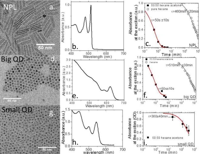
The first motivation of this work is the use of electrophoresis as a scalable and selective process for the cleaning of NPL. The achievement of selectivity will be based on the difference of electrophoretic mobility of the NPL compared to the other present species. As a first step we consequently conduct a kinetic study of the ED where pure populations of nanocrystals are used. We tested three populations of CdSe based particle: NPL, as well as small (3nm) and big (6nm) spherical quantum dots, see Figure 2a.b.d.e.g and h for TEM and absorption spectra. In particular, the small QD have been chosen as a model system of the side product resulting from the NPL synthesis, see Figure 1a.
Figure 2 a.b.c are respectively TEM image, absorption spectrum and kinetic studies (i.e.
absorption at the first exciton as a function of time) for CdSe NPL. d.e.f. are the same as
a.b.c. for CdSe big QD. g.h.i. are the same as a.b.c. for CdSe small QD.
The kinetic study of the ED is processed by dipping two copper electrodes in a solution of nanoparticles. The solvent is either hexane only or a mixture of hexane and acetone. The applied voltage is typically 400V for a 5mm spacing of the electrodes (equivalent electric field of 0.8kV.cm-1).
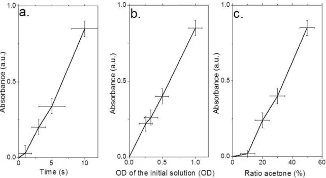
deposited material in the early stages of the ED a linear dependence can be seen of the amount of deposited material with time and concentration, see Figure 3a and b. On the other hand, the dynamic of deposition is strongly dependent on the presence of polar-solvent, see Figure 2c and Figure 3c. The exponential fit of the decay of the absorbance during the ED is 7.6h in pure hexane and is reduced to less than a minute in a 50:50 hexane:acetone mixture. The role of the polar solvent is not completely elucidated, but it is clear that its presence (i) tunes the dielectric constant of the medium, (ii) favors the presence of ions, in particular the dissociation of the carboxylic acid into carboxylate (iii) and leads to some aggregation of the nanoparticle as confirmed by the size change observed by the dynamic light scattering measurement see, figure S3. At low acetone concentration the film thickness slowly increases due to the rise of the dielectric constant of the solvent. Above 15% of acetone the slope gets stiffer which is related to the aggregation of the NPL.
Figure 3 Evolution of the thickness of the film of NPL made by electrophoresis as a function of
the time (a - applied bias is 400V, ratio acetone 50% and deposition time is 10s), initial
concentration of particle (b - applied bias is 400V, ratio acetone 50% and OD at the exciton
peak is 1), acetone ratio (c -applied bias is 400V, deposition time 10s and OD at the exciton
peak is 1).
We can relate the ED time constant to the electrophoretic mobility using the relation
, where A is the area of the electrodes, E the electric field between the electrodes, and V the volume of the solution. We estimate that the mobility is of the order of 1x10⁻⁴cm2V-1s-1 for the NPLs and large
QD in presence of non-solvent (50:50 hexane acetone mixture) while a value of 5x10⁻⁷cm2V-1s-1 is
obtained for the small QDs, in the same solvent. These estimations of the mobility are further confirmed within a decade while performing direct measurement of mobility using a ζ-meter, see table S1. The limited quantitative difference very likely results from the electric field dependence of the mobility which is much higher in our setup compared to the one applied in the ζ-meter.
V
E
A
µ
=
/
1
Our process is an electrophoretic deposition, performed with DC bias, and not a dielectrophoretic deposition31 that requires alternating current. The selection process is thus related to the charge of
the nanoparticles and not to their polarization. To be more precise, in a permanent electric field, the mobility µ, of nanoparticles with diameter a and a
z
-potentialz
, in a solution of dielectric constante
, and viscosityh
is given by the following equation32:(
)
D a f µ
/ 3 2 = , where f is the Henry’s
function37 which depends on a the diameter of the nanoparticles and on
l
D, the Debye length. For a
given solvent, the mobility of the nanoparticles, and thus the selectivity of the ED depends on the particles charge but also on the Henry’s function. Since f ranges between 1 and 1.5 while the ratio
D
a/
ratio is tuned, it is clear that the large change of mobility between big and small QD mostly results from a change ofz
value. The direct measurement of thez
-potential using az
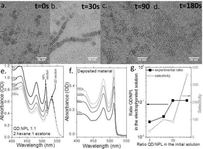
-meter confirms that indeed all particles have a slightly negative ζpotential ranging from 10mV for NPL to -2mV for small QD, see figure S3d and table S1.Figure 4 a-d are TEM images of mixtures initially made of small CdSe QD and CdSe NPL at
different time of the electrophoresis. The applied bias is 400V. The solvent is made of hexane
(66%) and acetone (33%). e and f are the absorption spectra made at different times
respectively from a mixture initially made of small CdSe QD and CdSe NPL and from the
redispersed material. g. Evolution of the ratio of QD over NPL population (measured by the
ratio of the optical density at the exciton peak) for the electrophoreted material (redispersed
in hexane) as a function of the ratio of QD and NPL in the initial solution. The selectivity of
the process is also plotted. The solvent is hexane:acetone 50:50. The applied bias is 400V.
Electrophoresis of a mixture
As a next step toward the selective cleaning of NPL, we perform the ED process on a mixture of NPL and small QD, which again have their size fitting with the side product obtained during the NPL synthesis. We start by a 1:1 (in absorbance) NPL:QD mixture. A TEM image of the mixture is given on Figure 4a. The absorption spectrum (Figure 4e) of the solution in particular displays two distinct features related to the QD (first absorption peak at 550nm) and to the NPL (first absorption peak at 510nm). We follow the ED process by TEM imaging and optical absorption, see Figure 4a-e and S4. As the ED occurs the peak related to the NPL decreases in magnitude, while the one related to the QD is barely affected. This is consistent with the fact that the NPL aggregate on the electrodes and little by little are removed from the initial mixture. This speculation is confirmed by redispersing the deposited material in pure hexane. The yield of the deposition is high (>95%), see figure Figure 4e and f and has been conducted successfully up to gram scale synthesis. The optical absorption of the deposited material, see Figure 4f, only shows the peaks related to NPL. Moreover the magnitude of the first absorption peak is consistent with a full extraction of the NPL from the initial mixture. We thus demonstrate that the ED can be used as a selective method to sort nanoparticles. We then tune the NPL:QD ratio and follow this ratio for the deposited material, see Figure 4g. The selectivity of the method is still observable even when NPL are introduced in minor quantity. Defining a selectivity as
, we obtain a value for S as high as 400, consistent with the ratio of
the deposition time observed on Figure 2.
We have also tested the ability to separate NPLs from QDs directly after the synthesis. In this case, the spherical QDs are a by product of the reaction performed to obtain a majority of NPLs. The reaction mixture may also contain unreacted precursors, excess ligands and a mixture of non-polar solvents. In spite of this complexity we have been able to obtain a pure deposition of NPLs, see Figure 1a. The fact that this method can be performed on the crude mixture of NPL synthesis is very promising to achieve upscaling of the NPL synthesis. The NPLs that are selected using ED remains photo-luminescent, see Figure S5. However, compared to the NPLs cleaned with the usual precipitation method we observe a loss of the PL signal and an increase of the deep trap emission. We attribute these observations to the fact that the ED process is non-neutral toward the capping ligands and probably remove them from the surface of the nanoparticles, leaving the surface charged and thus raising the absolute ζ-potential. This speculation is confirmed by the drop of the PL efficiency while cycling the electrophoresis step and the fastening of the deposition, see figure S5. Electrophoresis of NPL with different thicknesses is also possible but it is not very clear whether the difference result from thickness or lateral extension difference while doing the experiment with CdSe core only. Indeed NPL 510 typically have a 4 monolayers thickness with a lateral size of 10x40nm (see figure 2a) while NPL 460 have a 3 monolayers thickness but a lateral size of hundred nm (see figure
initial deposited
QD
of
amount
NPL
of
amount
QD
of
amount
NPL
of
amount
S
=
S1). Consequently the NPL 460 are not colloidally stable and are deposited much faster by electrophoresis. In order to check the possibility to use electrophoresis to sort NPL of different thicknesses we grow a CdS shell on CdSe NPL38 and we obtain NPL with different thickness and
similar lateral size. It appears that the thinner NPL tends to be deposited faster, see figure S6.
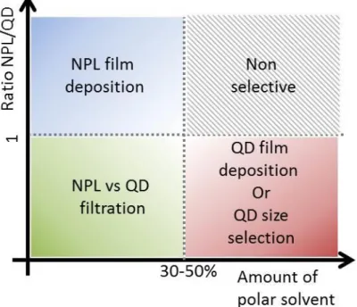
Figure 5 Phase diagram of the possible applications for electrophoresis of a NPL and QD
mixture as a function of polar solvent amount and ratio of NPL vs QD.
Phase diagram for the deposition of a QD:NPL mixture
In conclusion, for a given solvent, the difference in mobility between nanoparticles (and thus the selectivity during the ED process) depends on the product
z
f a /
(
l
D)
where gives the main modulation. The experiments we have performed with different types of nanoparticles and different solvents can be partially summarized in the phase diagram presented in Figure 5. When a mixture of QD and NPLs is electrodeposited, three different regimes can be identified. At low ratio of NPL/QD, and low amount of polar solvent efficient selection of NPL vs QDs can be achieved. At high ratio of NPLs, homogeneous deposition of NPLs films on large area can be rapidly obtained. When mostly spherical QDs are present in the solution, rapid ED of QDs can be performed when the solvent is highly polar. When the polar solvent is absent, QD size selection can be performed, but at the price of long deposition time.Electrophoresis for film deposition of NPL
The use of ED to obtain films made of spherical QDs and nanorods shaped materials have already been documented16-20. In the following we test the potential of NPL ED to achieve thick film
deposition (thickness of the order of 1µm).
Figure 6 (a) image of an electrophoreted film of NPL, the scale bar is in cm. (b) SEM image of
an electrophoreted (and scratched) film of NPL. Some thickness and roughness measurement
are added. The highlighted profiles correspond to the two lines on the image. The inset is an
SEM picture around the groove (c) Absorption spectrum of a film of NPL made of a layer of
CdSe NPL 460, CdSe NPL 510 and CdTe NPL 500.
In Figure 6(a), we show a film obtained with the ED of 40nmx10nm of CdSe NPLs on a substrate with centimeter scale. The quality of the film is probed using a profilometer and scanning electron microscopy imaging. The typical roughness of the film is around 40-60nm, see Figure 6 (b) and its insets. This value is a trade-off with the deposition time. Smoother films can be achieved at the price of a longer deposition time. We also use ED to grow a multilayer system made of three different materials: CdSe NPL 460, CdSe NPL 510 and CdTe NPL 500. By adjusting the thickness of each layer we have been able to achieve a high pass filter (in wavelength) with a sharp transition due to the narrow transition of the NPL and an almost flat response on the absorbing side, see Figure 6 (c).
CONCLUSION
We demonstrate that ED can be used as a selective method to sort nanoparticles as a function of their shape and size. Moreover ED can be used to sort complex mixtures such as the one obtained at the end of a colloidal synthesis. Compared to other existing preparative methods, ED offers an easier path for the post sorting use of the nanoparticles. The surface charge is the main parameter driving the selectivity of the ED far above the size. A phase diagram as a function of the ratio of non-solvent and ratio of the nanoparticles present describing the application of ED is also proposed. Finally we also point out the strong potential of ED for large scale and homogeneous film deposition. Possible application as a narrow cut-off wavelength filter is also demonstrated.
ACKNOWLEDGEMENTS
We are grateful to X. Xu for performing the TEM measurements. BD thanks the ANR agency for funding. This work has been supported by the Region Ile-de-France in the framework of DIM Nano-K.
Supplementary material
Supplementary material includes details about the precursor and the nanoparticles synthesis. It also includes DLS and ζ-potential measurement. The effect of the ED on the PL is also given. This information is available free of charge via the Internet at http://pubs.acs.org/.
REFERENCES
1 Reiss, P.; Protiere, M.; Li, L. Small 2009, 5, 154-168.
2 Murray, C. B.; Norris, D. J.; Bawendi, M. G. J Am Chem Soc 1993, 115, 8706-8715. 3 Yin, Y.; Alivisatos, A. P. Nature 2005, 437, 664-670.
4 Morris-Cohen, A. J.; Malicki, M.; Peterson, M. D.; Slavin, J. W. J.; Weiss, E. A., Chem Mater 2013, 25,
1155-1165.
5 Chemseddine A., Weller H., Ber. Bunsenges, Phys. Chem. 1993, 97, 636-638.
6 Arnold, M. S.; Green, A. A.; Hulvat, J. F.; Stupp, S. I.; Hersam, M. C. Nat. Nanotechnol. 2006, 1, 60-65. 7 Stürzl, N.; Hennrich, F.; Lebedkin, S.; Kappes, M. M. J. Phys. Chem. C 2009, 113, 14628-14632.
8 Mastronardi, M. L.; Hennrich, F.; Henderson, E. J.; Maier-Flaig, F.; Blum, C.; Reichenbach, J.; Lemmer, U.;
Kubel, C.; Wang, D.; Kappes, M. M.; Ozin, G. A J Am Chem Soc 2011, 133, 11928-11931.
9 Fischer, C. H.; Weller, H.; Katsikas, L.; Henglein, Langmuir 1989, 5, 429-432.
10 Fischer, C. H.; Weller, H.; Fojtik, A.; Lumepereira, C.; Janata, E.; Henglein, A. Ber Bunsen Phys Chem 1986, 90,
46-49.
11 Shen, Y.; Gee, M. Y.; Tan, R.; Pellechia, P. J.; Greytak, A. B. Chem Mater 2013, 25, 2838-2848. 12 Pinaud, F.; King, D.; Moore, H. P.; Weiss, S. J Am Chem Soc 2004, 126, 6115-6123.
13 Sperling, R. A.; Liedl, T.; Duhr, S.; Kudera, S.; Zanella, M.; Lin, C. A. J.; Chang, W. H.; Braun, D.; Parak, W. J. Size
J. Phys. Chem. C 2007, 111, 11552-11559.
14 Eychmuller, A.; Katsikas, L.; Weller, H. Langmuir 1990, 6, 1605-1608.
15 Mamedova, N. N.; Kotov, N. A.; Rogach, A. L.; Studer, J. Nano Letters 2001, 1, 281-286. 16 Islam, M. A.; Herman, I. P Appl Phys Lett 2002, 80, 3823-3825.
17 Ahmed, S.; Ryan, K. M. Adv Mater 2008, 20, 4745-4750.
18 Song, K. W.; Costi, R.; Bulovic, V., Adv Mater 2013, 25, 1420-1423.
19 Benehkohal, N. P.; Gonzalez-Pedro, V.; Boix, P. P.; Chavhan, S.; Tena-Zaera, R.; Demopoulos, G. P.; Mora-Sero,
I. J. Phys. Chem. C 2012, 116, 16391-16397.
20 Santra, P. K.; Kamat, P. V. J Am Chem Soc 2013; 135, 877–885
21 Bass, J. D.; Ai, X.; Bagabas, A.; Rice, P. M.; Topuria, T.; Scott, J. C.; Alharbi, F. H.; Kim, H. C.; Song, Q.; Miller, R.
D., Angew Chem Int Edit 2011, 50, 6538-6542.
22 Singh, A.; English, N. J.; Ryan, K. M. J Phys Chem B 2013, 117, 1608-1615.
23 Dickerson, J. H., Electrophoretic Deposition of Nanocrystals in Non-polar Solvents. In Electrophoretic
deposition of nanomaterials, Springer 2012, 131-155.
24 Ithurria, S.; Dubertret, B. J. Am. Chem. Soc. 2008, 130, 16504-16505.
25 Ithurria, S.; Tessier, M. D.; Mahler, B.; Lobo, R. P. S. M.; Dubertret, B.; Efros, A. L. Nat. Mater. 2011, 10,
936−941.
26 Son, J. S.; Wen, X. D.; Joo, J.; Chae, J.; Baek, S. I.; Park, K.; Kim, J. H.; An, K.; Yu, J. H.; Kwon, S. G.; Choi, S. H.;
Wang, Z. W.; Kim, Y. W.; Kuk, Y.; Hoffmann, R.; Hyeon, T. Angew Chem Int Edit 2009, 48, 6861-6864.
27 Joo, J.; Son, J. S.; Kwon, S. G.; Yu, J. H.; Hyeon, T. J Am Chem Soc 2006, 128, 5632-5633.
29 Li, Z.; Peng, X. G. J Am Chem Soc 2011, 133, 6578-6586.
30 Bouet, C.; Mahler, B.; Nadal, B.; Abecassis, B.; Tessier, M. D.; Ithurria, S.; Xu, X. Z.; Dubertret, B. Two- Chem
Mater 2013, 25, 639-645.
31 Tessier, M. D.; Javaux, C.; Maksimovic, I.; Loriette, V.; Dubertret, B. ACS Nano 2012, 6, 6751-6758.
32 E. Lhuillier, S. Pedetti , S. Ithurria, H. Heuclin, B. Nadal, A. Robin, G. Patriarche, N. Lequeux and B. Dubertret, ,
ACS nano 2014, 8, 3813-3820.
33 E. Lhuillier, A. Robin, S. Ithurria, H. Aubin, B. Dubertret, Nano Lett 2014, 14, 2715-2719. 34 Yang Y.A.; Wu H.; Williams K.R.; Cao Y.C. Ang. Chem. 2005,117, 6870–6873.
35 Bouet C. ; Mahler B. ; Nadal B. ; Abecassis B. ; Tessier M.D. ; Ithurria S. ; Xu X. ; Dubertret B Chem. Mater.
2013, 25, 639–645.
36 Pedetti S.; Nadal B. ; Lhuillier E. ; Mahler B. ; Bouet C. ; Abécassis B. ; Xu X. ; Dubertret B., Chem. Mat 2013,
25, 2455–2462.
37 Henry, D. C.,. Proc. R. soc. Lond. Ser. A-Contain. Pap. Math. Phys. Character 1931, 133, 106-129.