HAL Id: hal-01122582
https://hal.archives-ouvertes.fr/hal-01122582
Submitted on 4 Mar 2015HAL is a multi-disciplinary open access archive for the deposit and dissemination of sci-entific research documents, whether they are pub-lished or not. The documents may come from teaching and research institutions in France or abroad, or from public or private research centers.
L’archive ouverte pluridisciplinaire HAL, est destinée au dépôt et à la diffusion de documents scientifiques de niveau recherche, publiés ou non, émanant des établissements d’enseignement et de recherche français ou étrangers, des laboratoires publics ou privés.
Passivation of InP(100) substrates: first stages of
nitridation by thin InN surface overlayers studied by
electron spectroscopies
Matthieu Petit, Christine Robert-Goumet, Luc Bideux, Bernard Gruzza, V
Matolin, S Arabasz, B Adamowicz, D Wawer, M Bugajski
To cite this version:
Matthieu Petit, Christine Robert-Goumet, Luc Bideux, Bernard Gruzza, V Matolin, et al.. Passi-vation of InP(100) substrates: first stages of nitridation by thin InN surface overlayers studied by electron spectroscopies. Surface and Interface Analysis, Wiley-Blackwell, 2005, 37 (7), pp.615-620. �10.1002/sia.2045�. �hal-01122582�
Passivation of InP (100) substrates: first stages of nitridation by thin InN
surface overlayers studied by electron spectroscopies.
M. Petita* C. Robert-Goumeta, L. Bideuxa, B.Gruzzaa, V. Matolina,b
S. Arabaszc, B. Adamowiczc, D. Wawerd, M. Bugajskid.
aLASMEA UMR CNRS 6602, Blaise Pascal University, 63177-Aubière Cedex, France
bDepartment of Electronics and Vacuum Physics, Charles University, V Holesovickach 2, 180
00 Prague 8, Czech Republic
cDepartement of Microelectronics, Institute of Physics, Silesian University of Technology,
Krzywoustego 2, 44-100 Gliwice, Poland
dInstitute of Electron Technology, Al. Lotnikow 32/46, 02-668 Warsaw, Poland
*corresponding author: tel +33 4 73 40 51 62, fax +33 4 73 40 73 40 e-mail: petit@lasmea.univ-bpclermont.fr
Abstract: This article investigates the nitridation effect of InP(100) semiconductor surfaces performed by a glow discharge cell (GDS). Electron spectroscopies (AES, ESCA) were used to understand the different steps of this process. An important point is the initial quantity of metallic indium on the InP(100) surfaces. Indeed the indium droplets, created in well known quantity, play the role of precursor. At a relatively low temperature T = 523 K, the system undergoes surface restructuration which includes removal of the In droplets and the elaboration of two InN monolayers. P-N bonds and In-N bonds have been detected by the analysis of PLMM and InMNN Auger peaks and In4d ESCA peak. However, the presence or not of
metallic indium inside this InN overlayer is crucial for the passivation of the substrate. Ex-situ photoluminescence measurements correlated to the electron spectroscopies results have put in
evidence the good passivation effect of the InP(100) surfaces by InN overlayers for 40 minutes of nitridation.
PACS: 68.49Uv ; 68.55Jk ; 79.60Dp ; 61.46.+w ; 78.55.-m
Keywords: indium nitride, indium phosphide, nitridation, electron spectroscopies, AES, ESCA, photoluminescence, passivation.
INTRODUCTION
III-V compound semiconductor surfaces and interfaces have been intensively investigated in the past decades because of both fundamental and technological interest. Among them indium phosphide is known to have a high carrier mobility : this material have a strong potential use in integrated optoelectronic devices [1].
Treatments of indium phosphide surfaces will improve temporal and thermal stability of devices developed on the base of this semiconductor. Designed technology of III-V nitridation can have considerable importance for modern electronics, optoelectronics, quantum devices and other devices with nanometer sizes.
However the nitridation of III-V semiconductors is quite difficult because of the small sticking probability of nitrogen on the surface [2]. For InP, several kinds of nitridation process have been used to produce nitridated films: among them, alkali metals promoted nitridation which lead to the formation of mainly InPNx layers [3,4], direct nitrogen ion beam nitridation
resulting in nitridated layers showing In-N, In-N-P and P-N bondings [2] and plasma nitridation which entails the creation of In-N and P-N bonds [5].
In this article, we are focused on the first steps of InP (100) nitridation following at a low scale by electron spectroscopies (AES, ESCA). The reactive nitrogen beam was produced by a high voltage glow discharge source (GDS) with two incident angles : normal and grazing to the normal of the surface. Results by photoluminescence ex-situ method obtained on the InN/InP ended structures are also reported. The InP(100) surfaces have been firstly bombarded by argon ions to remove contamination layers but this cleaning produce a preferential phosphorus desorption which entails the creation of metallic indium droplets (coverage rate 25%, average height : 4 monolayers) [6]. This method based on an indium precursor state has been fruitfully used to create InN atomic layers. Clearly passivation of the InP substrates was observed underlining the efficiency of the process.
EXPERIMENTAL
Two ultra vacuum chambers (10-7 Pa) have been used for this study. One was equipped with
ESCA spectroscopy using the MgK radiation (1253,6 eV) and the analysis were performed
on ended InN/InP(100) structures. The other UHV chamber, having Auger electron spectroscopy (AES) and nitrogen source, was devoted to samples elaboration. During the nitridation process, Auger peaks can be recorded in real time.
Loading of the InP(100) substrates (S doped, n = 4,7 1016 cm-3) were done after ex-situ
chemically cleaning [7, 8]. This cleaning is based on successive baths of H2SO4, a solution of
3% bromine in methanol and deionised water. The sample surface is controlled by Auger electron spectroscopy with a retarding field analyser.
a) Indium based precursor state.
After introduction of the samples in UHV chamber, a low level contamination by carbon and oxygen was detected. These impurities were removed in situ by Ar+ ions bombardment using
a low energy (E0 = 300 eV, ion current = 2 A cm-2 , t = 15 min). This first treatment induces
P depletion and well controlled metallic indium islands formation [9,10]. These nano-droplets on the surface have been extensively studied in the past by authors using mainly electron spectroscopies and simulation for a good understanding of the phenomenon [6,10,11]. It has been shown that roughly each crystallite contains about ten In atoms and the whole quantity of metallic indium is equivalent in coverage to one monolayer [6]. Atoms of V element as antimony deposited on this In rich surface induce 3D 2D transformation and the formation of thin InSb overlayers [12,13].
Under heating (T = 573 K) one also clearly observes the vanishing of In droplets [10,14] which would appear again if the temperature decreases up to 300 K.
In this study we have advisedly used the indium rich InP(100) surfaces and the heating effect to include nitrogen atoms in the overlayer region.
b) Nitridation process.
The reactive nitrogen beam was produced by a high voltage glow discharge source (GDS). This kind of source mainly creates nitrogen atoms, with some N+, N2+ and N
2 species in very
low amount. Two directions of the nitrogen flow were possible: a grazing incidence or a normal one to the surface sample. Time was a fundamental parameter of the nitridation. Another one was the temperature fixed equal to T = 523 K which was optimal for the process because the decomposition temperature of InP is around T = 573 K.
RESULTS AND DISCUSSIONS.
a) A.E.S. analysis :
The nitridation of the In rich InP surface was followed by recording the Auger peaks of the three atomic elements:
- P LMM (E = 117 eV) - N KLL (E = 383 eV)
- In MNN (E = 403 eV and 411 eV)
The RFA apparatus gives best results for low electron kinetic energies. For this reason phosphorus Auger peak has been well observed. On the other hand, the evolution of intensities gives important information along the duration of the process. Concerning the knowledge on the environment of indium atoms, better results were obtained with XPS spectroscopy and are presented in the following part of this article.
In the figure 1 one has reported the ratio N P I
I of the Auger signal intensities of nitrogen and phosphorus atoms respectively. Clearly for a grazing incidence flow the nitridation seems better because of the increase of the N Auger peak and the decrease of the phosphorus signal.
Really the mode of preparation with a liquid indium layer on the surface acting as a precursor plays an important role. In the literature [15,16] we can find opposite results concerning influence of the beam direction on other initial kind of InP surface. In their case, the nitridation process is performed by ion gun method. As regard us, the explanation is simply due to the longer path trajectory of incident N atoms in the indium overlayer.
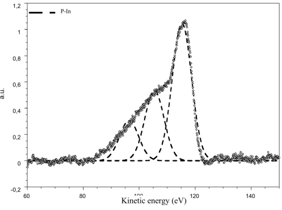
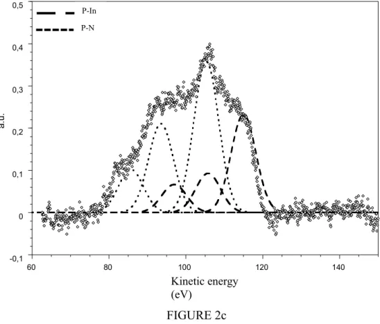
In the figures 2 (a, b, c) the Auger spectra of phosphorus are presented for several nitridation times (t=0, 20 and 40 min) with the decomposition into three components which represent the Auger transitions LMM [17]. These transitions, including the valence atomic level L, are very sensitive to the surrounding of P atoms. During the nitridation, the Auger peak shape is changing and one observes the contribution of nitrogen surrounding (P-N bonding). The figure 2c (t = 40 min) indicates a more important contribution of P-N in comparison to that of P-In. Following this idea we have reported in the figure 3 the ratio:
ons contributi In P of Total ons contributi N P of Total R
which gives information on the proportion of created P-N bonds compared to P-In bonds. Three areas are observed for the two nitridation angles:
- the region 1: the beginning of the nitridation
- the region 2: the optimisation of the nitridation (the maximum for R) - the region 3: a decrease of the factor R
From this graph one can deduce the time to create a complete InN overlayer, which must be equal to 40 minutes for both the two possible directions of the N beam. Considering the evolution of these two lines it is more continuous in the case of grazing incidence, one must also have in mind the figure 1 indicating more nitrogen adsorption in this case. Moreover in spite of a smaller maximum the curve is above the other one. For these reasons we can consider a better efficiency for grazing incidence N flux.
Concerning the indium M4N45N45 one remarks an energy shift of the peak which is maximum
(E = 2 eV) for t = 40 min and also with the use of a grazing nitrogen beam. This result must be correlated to the optimisation of the nitridation of the sample.
b) ESCA results :
Looking at the photoelectron spectra of In4d level presented in the figure 4, a shift of this peak
is observed versus the nitridation time. This shift is equal to 0.8 eV for t = 20 min and maximum (2 eV) for t= 40 min. Prolonged time of nitridation (t = 60 min) implies a diminution of this shift (1 eV). In fact these results must be compared to those from the figure 3 where three steps for the nitridation process have been put in evidence.
More precisely, the XPS analyses are reported in the spectra series of the figures 5. Remembering that indium 4d peak is due to a double contribution (4d3/2, 4d5/2) it is possible to
decompose each experimental peak recorded at different times of nitridation. The contributions of oxides –present on the surface since the samples have been exposed to the atmosphere during the transfer from one UHV chamber to the other to perform XPS analysis-were not included in the figure for a readable question.
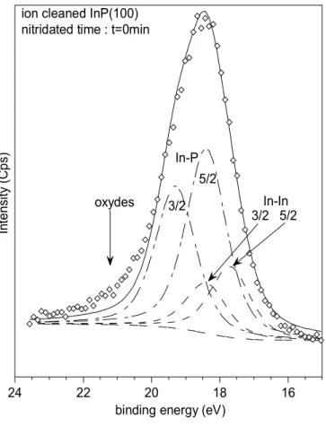
At the beginning (t = 0 min) only In-P contribution (18.5 eV and 19.5 eV) and In-In contribution due to the initial droplets (17.5 eV and 18.5 eV) are present (figure 5a). After 20 minutes of nitridation, we observe a decrease of the In-In peaks and the apparition of a new contribution at E = 19.5 eV and 20.5 eV characteristic of the In-N bonds [17] (figure 5b). The time t = 40 minutes corresponds to the time for a complete nitridation of the substrate, no more metallic indium is present on the surface (figure 5c). When the experiment is prolonged (t = 60 min) one observes again the presence of In-In peaks (figure 5d).
c) Interpretation attempt
From the previous results one can deduce that nitridation experiment follows two steps. In the first times, we observe the nitridation of the surface up to a complete consummation of initial quantity of free indium which is liquid on the surface at T = 523 K. Then the correct time of
the process is close to 40 minutes for which a maximum of two InN monolayers have been condensed on the surface. The initial state of In crystallites on InP is well known: mean sizes 4 monolayers and coverage 25%. The two nitrided monolayers are corresponding to the maximum of possible stacking layers with an initial quantity of metallic indium equal to one monolayer.
At this time the nitridation is stopped due to the lack of free indium atoms. An irreversible process is observed coming with the apparition of In-In bonds. A possible satisfying explanation can be a low desorption of InN at this temperature and a damage of the surface. This phenomenon is comparable to the evaporation of InP substrate (congruence temperature 573 K) [18]. The schematic figure 6 summarises the nitridation process in time.
EX-SITU PHOTOLUMINESCENCE EXPERIMENTS :
Room temperature ex-situ photoluminescence measurements upon different excitation light intensities from InP samples after nitridation were carried out at the Institute of Electron Technology (Warsaw, Poland). The green line (514.5 nm) of Ar+ laser was used as an
excitation source. The photoluminescence signal was collected by an optical fibre and analysed by a spectrometer equipped with a CCD camera.
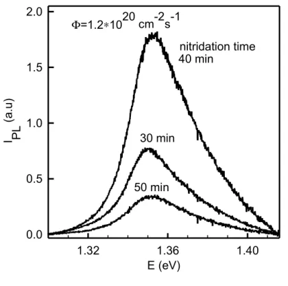
A set of near-band edge PL spectra for 30, 40 and 50 minute nitrided InP(100) surfaces is shown in Fig. 7a. It is clear that PL intensity (IPL) varies markedly after different nitridation
times although no change in spectrum shape was observed. The strongest photoluminescence was found for the sample after 40 min nitridation. Recently, we proved that PL is affected by highly complicated surface recombination processes [19] and is a strongly nonlinear function of both excitation light intensity, and surface state distribution [20]. Thus, in order to assess the recombination properties of InN-InP interface, PL measurements at different excitation light intensities () were performed. The results, in terms of a PL quantum efficiency, i.e. ratio YPL=IPL/ for various nitridation time are summarised in Fig. 7b. The significant
increase of YPL (by about half an order of magnitude upon high ) is observed for 40 minutes
nitridation in comparison to 30 and 50 minutes processing. We attribute this increase to the decrease of interface recombination rate, probably due to the reduction of interface state density. This hypothesis is additionally supported by the fact that the largest dynamics of YPL
changes upon increasing is also noticed for 40 minutes nitridation. It is well explained in terms of the gradual saturation of interface states as non radiative interface recombination centers [20]. Apparently, the smaller interface state density coincides with the faster saturation, and thus with better-marked YPL changes. So that, nitridation for 40 minutes yields
the best passivation effect of InP substrate by InN overlayer.
It should be emphasised that the PL-based characterisation of InN-InP interface is well consistent with the analysis of electron spectroscopy results. From comparison of Fig. 7b and Fig.3 it is clear that the YPL behaviour follows the amount of nitrogen content at the interface,
indicating different mechanism of nitridation. Therefore the correlation between the electronic properties and the chemical composition of the interface is evident.
CONCLUSION
The formation of metallic indium on the InP(100) by Ar+ bombardment is a precursor for
formal elaboration of InN monolayers on the substrate. Experimental choices of parameters are crucial. The temperature T = 523 K seems the best one and well allows the inclusion of nitrogen atoms. Time around 40 minutes is really optimal, all metallic indium is consumed and the process must be stopped. Better efficiency is obtained when the nitrogen beam has grazing incidence. Electron spectroscopies (AES, ESCA) give quantitative results at the nano-scale, the knowledge of the structure InN/InP(100) is absolutely necessary to well understand ex-situ analysis. Optical measurements are well correlated to the quality of sample nitrided overlayer. Passivation of the semiconductor surface has been really put in evidence by such kind of experimental results. Some complementary experiments (LEED) must be performed
to conclude on the crystallinity of the InN overlayers. Such sort of heterostructures is promising substrates for optoelectronics and nanoelectronics. One of the future objectives is the use of an indium evaporation source in order to have also the possibility to increase the thickness of InN overlayer.
ACKNOWLEDGEMENTS
This work was partially performed within the V FPEC Project of Centre of Excellence in Physics and Technology of Semiconductors Interfaces and Sensors (CESIS) under the contract G6MA-CT-2002-04042. One of the author (S.A.) acknowledges the Marie Curie Host Fellowship funded by the European Commission.
REFERENCES
1. S. M. Sze, « Physics of Semiconductor Devices », 2nd Ed (Wiley, New York 1981)
2. Y. Suzuki, H. Kumano, W. Tomota, N. Sanada, Y. Fukuda, Appl. Surf. Sci. 2000; 162-163: 172
3. P. Soukiassian, H.I. Starnberg, T. Kendelwicz, Appl. Surf. Sci. 1992; 56-58 : 772 4. H.I. Starnberg, P. Soukiassian, T. Kendelwicz, Surf. Sci. 1992; 269/270: 915 5. M. Losurdo, P. Capezzuto, G. Bruno, E.A. Irene, J. Vac. Sci. Technol. A 1999; 4:17 6. B. Gruzza, C. Pariset, Surf. Sci. 1991 ; 247 : 408
7. D. Gautard, J.L. Laporte, M. Cadoret, C. Pariset, J Crystal Growth 1985; 71:125 8. L. Bideux, B. Gruzza, A. Porte, Surf. Interface Anal., 1993 ; 20 : 803
9. J.C. Tsang, A. Khan, P. Mark, Surf. Sci., 1980 ; 97 : 119
10. S. Abdellaoui, B. Gruzza, C. Pariset, M. Bouslama, C. Jardin, D. Robert, Surf. Sci. Lett. , 1989 ; 208 : L21
11. B. Gruzza, A. Porte, L. Bideux, C. Jardin, J. Miloua, Act. Phys. Polonica A 1992 ; 81 : 223 12. B. Gruzza, C. Pariset, S. Abdellaoui, Surf. Interface Anal. 1990 ; 16 : 54
13. P. Soukassian, P. S. Mangat, Y. Huttel, Z. Hurych, B. Gruzza, A. Porte, J. Vac. Sci.
Technol. B 1993; 11 : 1603
14. B. Gruzza, Thesis of Blaise Pascal University, Clermont-Ferrand II N° 389 (1987)
15. J. D. Hecht, F. Frost, T. Chassé, D. Hirsch, H. Neumann, A. Schindler, F. Bigl, Appl. Surf.
Sci. 2001; 179: 196
16. J.S. Pan, A.T.S. Wee, C.H.A. Huan, K.I. Tan, J. Phys. D Appl. Phys., 1996; 29: 2997 17. Y. Ould-Metidji, L. Bideux, V. Matolin, B. Gruzza, C. Robert, Vacuum, 2001; 63 : 229 18. R.F.C. Farrow, J. Phys. D Appl. Phys. 1974; 7: L121
19. B.Adamowicz, H. Hasegawa, Jpn.J.Appl.Phys., 1998; 37:1631 20. B. Adamowicz, H. Hasegawa, Thin Solid Films 2002; 367: 180
FIGURE CAPTIONS
Figure 1: Ratios of Auger signals of nitrogen and phosphorus atoms versus nitridation time and for two positions of the N beam.
Figure 2a: Phosphorus Auger transition after in-situ cleaning of the InP substrate.
Figure 2b: Phosphorus Auger transition after 20 minutes of nitridation. The decomposition in series of triplets indicates the presence of P-N bonds.
Figure 2c: Phosphorus Auger transition after 40 minutes of nitridation. The decomposition in series of triplets indicates the presence of P-N bonds.
Figure 3: Ratio of the intensities of P-N and P-In Auger signals, showing the influence of the nitrogen beam direction. Versus time of nitridation, three regions are put in evidence
Figure 4: The indium 4d peak for different times of nitridation and the associated energy shift. Figure 5a: The decomposition of the In4d ESCA peak after the Ar+ cleaning showing the
metallic indium on the surface.
Figure 5b: The decomposition of the In4d ESCA peak after 20 minutes of nitridation. In-N bonds are apparent.
Figure 5c: The decomposition of the In4d ESCA peak after 40 minutes of nitridation. No more metallic indium detected.
Figure 5d: The decomposition of the In4d ESCA peak after 60 minutes of nitridation. A decrease of the In-N signal, a detection of metallic indium.
Figure 6:A schematic representation of the surface nitridation along duration of the process. Figure 7a: Room temperature photoluminescence spectra obtained on different nitrided InP substrates (constant light intensity = 1.2 1020 cm-2s-1)
Figure 7b: Quantum efficiency for various nitrided InP samples obtained with different light intensities .
FIGURE 1 0 5 10 15 20 25 30 0 8 16 24 32 40 48 56 64 N/P normal N/P grazing I N /I P
FIGURE 2a -0,2 0 0,2 0,4 0,6 0,8 1 1,2 60 80 100 120 140 a. u. eV P-In
FIGURE 2b -0,1 0 0,1 0,2 0,3 0,4 0,5 0,6 0,7 60 80 100 120 140 a. u. eV P-In P-N Kinetic energy (eV)
FIGURE 2c -0,1 0 0,1 0,2 0,3 0,4 0,5 60 80 100 120 140 a. u. eV P-In P-N Kinetic energy (eV)
FIGURE 3 0 0,4 0,8 1,2 1,6 0 10 20 30 40 50 60 70 Grazing flow Normal flow
nitridation time (min) P-N > P-In
P-N < P-In
Region 1 Region 2 Region 3
FIGURE 4 16 18 20 22 24 0 min 20 min 40 min 60 min In te n si ty ( C p s)
FIGURE 5a 16 18 20 22 24 In te ns ity ( C ps )
binding energy (eV) In-P 5/2 3/2 In-In 5/2 3/2 oxydes
ion cleaned InP(100) nitridated time : t=0min
FIGURE 5b 16 18 20 22 24 In te ns ity ( C ps )
binding energy (eV) In-N
In-P
In-In nitridated InP(100)
FIGURE 5c 16 18 20 22 24 In te ns ity ( C p s)
binding energy (eV) InP
InN
nitridated InP(100) t=40min
FIGURE 5d 16 18 20 22 24 In te ns ity ( C p s)
binding energy (eV) nitridated InP(100)
t=60min
InP
In-In In-N
FIGURE 7a =1.21020 cm-2s-1 E (eV) 1.32 1.36 1.40 I PL ( a. u) 0.0 0.5 1.0 1.5 2.0 50 min 40 min 30 min nitridation time
FIGURE 7b
nitridation time (min)
30 40 50