HAL Id: tel-03212304
https://tel.archives-ouvertes.fr/tel-03212304
Submitted on 29 Apr 2021HAL is a multi-disciplinary open access
archive for the deposit and dissemination of sci-entific research documents, whether they are pub-lished or not. The documents may come from teaching and research institutions in France or abroad, or from public or private research centers.
L’archive ouverte pluridisciplinaire HAL, est destinée au dépôt et à la diffusion de documents scientifiques de niveau recherche, publiés ou non, émanant des établissements d’enseignement et de recherche français ou étrangers, des laboratoires publics ou privés.
laser deposition
Yannick Bleu
To cite this version:
Yannick Bleu. Graphene and doped graphene elaborated by pulsed laser deposition. Materials Science [cond-mat.mtrl-sci]. Université de Lyon, 2020. English. �NNT : 2020LYSES033�. �tel-03212304�
N° ordre NNT: 2020LYSES033
THESE de DOCTORAT DE L’UNIVERSITE DE LYON
Opérée au sein du
Laboratoire Hubert-Curien
Ecole Doctorale N° 488
Sciences Ingénierie Santé SIS Spécialité: Science des matériaux
Soutenue publiquement le 09/10/2020 par :
Yannick Mexon BLEU
Graphene and doped graphene
elaborated by pulsed laser deposition
Devant le jury composé de :
Yann BATTIE Professeur, Université de Lorraine Rapporteur
Patrice MELINON DR CNRS, ILM – Université Claude Bernard Lyon 1 Rapporteur Anastasia TYURNINA Research Fellow, Brunel University London, UK Examinatrice Florence GARRELIE Professeur, Université Jean-Monnet Saint-Etienne Présidente de Jury Vincent BARNIER Ingénieur de Recherche, Ecole des Mines Saint-Etienne Invité
Florent BOURQUARD Maître de Conférence, Université Jean-Monnet Saint-Etienne Invité
José AVILA Ingénieur de Recherche, Synchrotron SOLEIL, Paris Co-directeur de thèse Christophe DONNET Professeur, Université Jean-Monnet Saint-Etienne Directeur de thèse
1 Remerciements ... 4 Warning ... 5 List of abbreviations ... 6 List of figures ... 8 List of Tables ... 14
Résumé de la thèse en français ... 15
General Introduction ... 20
Chapter 1: Graphene synthesis using pulsed laser deposition: State of art ... 25
I. Background on graphene ... 25
1. Graphene crystalline structure ... 25
2. Properties and potential applications ... 29
3. Graphene synthesis methods ... 32
II. Focus on Pulsed Laser Deposition (PLD) for graphene synthesis ... 39
1. General considerations ... 39
2. PLD graphene synthesis using a metal catalyst ... 42
3. Doped graphene synthesis using the PLD method ... 48
III. Conclusions ... 50
References ... 52
Chapter 2: Experimental methodology for graphene synthesis & characterization ... 64
I. Nickel catalyst and carbon precursor deposition process ... 64
1. Nickel thin film deposition by thermal evaporation ... 64
2. Amorphous carbon thin film deposition by laser ablation ... 65
II. Post deposition annealing: Rapid Thermal Annealing (RTA) ... 75
III. Physico-chemical and structural characterization methodologies ... 75
1. Profilometer ... 76
2. Raman spectroscopy ... 77
3. X-Rays photoelectron spectroscopy (XPS) ... 82
4. Ultraviolet-Visible spectrophotometry ... 84
5. Scanning Electron Microscopy (SEM) ... 85
6. Atomic Force Microscope (AFM) ... 86
7. Transmission Electron Microscopy (TEM) ... 87
2
Chapter 3: Mechanism of graphene growth by carbon diffusion-segregation through
nickel catalyst: an in situ XPS study ... 95
I. Experimental protocol ... 96
II. Morphology and microstructure analysis of the film after annealing ... 98
III. Carbon and nitrogen chemistry after diffusing across the nickel layer ... 99
IV. Carbon diffusion kinetics across the nickel catalyst film ... 103
V. Modeling of carbon diffusion and segregation through the nickel thin film ... 109
1. Modeling background ... 109
2. Modeling results ... 111
VI. Summary ... 113
References ... 115
Chapter 4: Parametric studies for the optimization of graphene synthesis by PLD and RTA ... 118
I. Effect and choice of suitable substrate, deposition sequence and annealing condition for the graphene synthesis ... 119
1. Substrate effect on the graphene growth ... 119
2. Effect of catalyst / amorphous carbon deposition sequence on graphene synthesis 129 II. The effect of the starting thickness of the amorphous carbon on graphene synthesis 132 1. Graphene layer number distribution through I2D/IG ratio mapping, as a function of the initial thickness of a-C and annealing temperature ... 132
2. Defects density distribution through ID/IG ratio mapping as a function of the initial thickness of a-C and annealing temperature ... 134
3. The optimal synthesis conditions and further analysis ... 135
III. The effect of the starting thickness of the nickel catalyst on graphene synthesis ... 141
1. Effect of rapid thermal annealing on the morphology of nickel thin film ... 143
2. Nickel thickness influence on the transformation of PLD amorphous carbon into graphene after thermal annealing at 900°C ... 148
3. The optimal synthesis condition and further characterizations ... 156
IV. Summary of the parametric study for graphene synthesis by PLD and RTA ... 160
References ... 163
Chapter 5: Boron doped graphene synthesis and electrochemical characterization ... 168
I. Introduction: why boron doping? ... 168
II. Experimental protocol to synthetize BG layers from a-C:B films ... 169
III. Structural and chemical analysis of the synthesized films ... 170
3
1. Cyclic voltammetry measurements of the as-grown graphene and boron-doped
graphene ... 176
2. Evaluation of the stability of the Boron doped graphene with 2.5 at. % ... 178
V. The relation between graphene nanostructures and their electrochemistry response . 180 VI. Summary ... 180
References ... 182
General conclusions and perspectives ... 184
4
Remerciements
Le travail présenté dans ce mémoire a été réalisé au sein du Laboratoire Hubert Curien (UMR 5516) de l’Université Jean Monnet de Saint-Etienne.
Cette thèse a été dirigée par M. Christophe Donnet et M. José Avila. Elle a été co-encadrée par Anne-Sophie Loir, Florent Bourquard et Vincent Barnier. Je les remercie vivement pour leur choix, leur aide et leur encadrement que j’ai beaucoup appréciés. J’exprime ici toute ma gratitude à l’ensemble de ce corps de direction et d’encadrement pour leurs compétences scientifiques, techniques, et leur dynamisme qui ont permis de mener à bien cette étude. Ils m’ont toujours soutenu tout en m’offrant beaucoup de liberté.
Je remercie Messieurs Yann Battie et Patrice Mélinon pour l’intérêt qu’ils ont accordé à mon travail en acceptant d’être rapporteurs, ainsi que Mme Anastasia Tyurnina et Mme Florence Garrelie qui m’ont fait l’honneur de faire partie de mon jury.
J’exprime toute ma gratitude au LABEX MANUTECH SISE qui a soutenu financièrement ma thèse. J’ai bénéficié de l’aide et des conseils de très nombreuses personnes au sein du Laboratoire Hubert Curien. Je tiens donc à remercier spécialement Jean-Yves Michalon qui m’a formé à l’utilisation de la machine de dépôts par évaporation ainsi qu’au spectromètre Raman. J’en profite pour remercier vivement Stéphanie Reynaud qui m’a formé à l’utilisation des microscopes MEB et AFM, sans oublier Yaya Lefkir pour les belles images HRTEM. Je voudrais également remercier Nicolas Faure pour son aide sur l’utilisation des lasers, le microscope optique et parfois au MEB. J’adresse également mes remerciements à Fred Celle pour sa disponibilité et sa formation à l’accès à la salle blanche ainsi qu’à l’utilisation du spin coater. Je remercie aussi Frédéric Christien (Mines St-Etienne) pour son modèle de diffusion qui a contribué largement au chapitre 3. Je tiens également à remercier Carole Chaix et Carole Farre de l’institut de sciences analytiques de Lyon pour les mesures d’électrochimie.
Ces 3 ans auraient été moins agréables sans la présence des autres doctorants du laboratoire. Je voudrais donc remercier Mathilde Prudent, Leïla Ben Mafhoud, Djaffar Iabbadden, Erieta Katerina Koussi, Yohan Bousset, et Maria Usuga. Je n’oublie pas non plus l’équipe informatique et le personnel administratif pour leur disponibilité.
5
Warning
Au cours de la 3ème et dernière année de ce travail de recherche doctoral, est survenue la pandémie liée au COVID-19. Cette situation s’est traduite par une fermeture des laboratoires de recherche entre mars et mai 2020, suivie par une période pendant laquelle les moyens expérimentaux ont été très progressivement rendus accessibles, mais selon des règles sanitaires limitant leur utilisation.
Cette période a coïncidé avec les derniers mois de nos travaux, ce qui a empêché de conduire certaines expériences prévues, en particulier l’optimisation du protocole de transfert des couches de graphène qui aurait permis de réaliser des images de microscopies électroniques par transmission dans des conditions idéales, ainsi que des mesures de propriétés de conduction électronique de nos échantillons de graphène pur et dopé au bore.
During the third and last year of this research work, the COVID-19 pandemic occurred. This situation resulted in a closure of the research laboratories between March and May 2020, followed by a period during which the experimental tools were very gradually made available, but according to health rules limiting their use.
This period coincided with the last months of our work, which prevented certain planned experiments from being carried out, in particular the optimization of the graphene transfer protocol which would have made it possible to perform more and better transmission electron microscopy images under conditions ideal, as well as measurements of electronic properties of our obtained graphene and boron doped graphene.
6
List of abbreviations
a-C: Amorphous Carbon ... 40
a-C:B: Boron doped amorphous carbon ... 73
a-C:N: Nitrogen doped amorphous carbon ... 69
AFM: Atomic Force Microscope ... 24
ASE: Amplified Spontaneous Emission ... 70
BG: Boron doped graphene ... 170
BLG: Bilayer Graphene ... 30
BSE: Backscattered Electron ... 87
CMOS: Complementary Metal Oxide Semiconductor ... 37
CNT: Carbon Nanotubes ... 22
CPA: Chirped Pulse Amplification ... 69
CV: Cyclic voltammetry ... 78
CVD: Chemical Vapor Deposition ... 23
DLC: Diamond-Like Carbon ... 22
EBSD: Electron Backscatter Diffraction ... 78
EDS: Energy Dispersive Spectroscopy ... 88
EG: Epitaxial Graphene ... 36
FCVA: Filtered Cathodic Vacuum Arc ... 39
FeCl3: Iron (III) Chloride ... 142
FET: Field Effect Transistor ... 33
FHWM: Full Half-Width Maximum ... 81
FLG: Few-layer Graphene... 30
FTO: Fluorine doped Tin Oxide ... 31
G: undoped graphene ... 179
GNPs: Graphene nanoplatelets ... 31
GRM: Graphene and related materials ... 22
HOPG: Highly Oriented Pyrolytic Graphite ... 27
HRTEM: High Resolution Transmission Electron Microscope ... 24
ISO: International Organization for Standardization ... 30
ITO: Indium Tin Oxide ... 31
KrF: Krypton Fluoride ... 69
LIBs: Lithium ion Batteries ... 33
LPE: Liquid Phase Exfoliation ... 38
MBE: Molecular Beam Epitaxy ... 39
MC: Mechanical exfoliation ... 34
NMP: N-methylpyrrolidone ... 38
ORR: Oxygen Reduction Reaction ... 51
PAPD: Pulse Arc Plasma Deposition ... 39
PECVD: Plasma Enhanced Chemical Vapor Deposition... 36
PLD: Pulsed Laser Deposition ... 23
PVD: Physical Vapor Deposition ... 39
7
RTA: Rapid Thermal Annealing ... 23
SEM: Scanning Electron Microscope ... 24
SiC: Silicon Carbide ... 34
SLG: Single Layer Graphene ... 30
STM: Scanning Tunneling Microscope ... 27
TEM: Transmission Electron Microscope ... 89
UHV: Ultra-High Vacuum ... 37
8
List of figures
Figure 0. 1 Illustration of the organization of the contents of this Ph.D. manuscript. ... 23 Figure 1. 1 Illustration of graphene as a mother of carbon allotropes and can be converted to fullerenes, carbon nanotubes, and graphite. Adapted from reference7. ... 26
Figure 1. 2 Illustration of the carbon sp2 hybridization: (a) its electronic structure comprises an s orbital and three p orbitals. (b) The sp2 hybridization consists of three sp2 orbitals and one pz orbital perpendicular to the other three, (c) triangular planar geometry, (d) π, and σ orbitals leading to the graphene lattice. ... 27 Figure 1. 3 (a) Graphene lattice representation: the two inequivalent atoms of the unit cell are highlighted with blue and red colors. (b) Graphene energy bands close to the Fermi level: the conduction and valence bands touch at K and K’ points. Adapted from11. ... 28
Figure 1. 4 Schematic stacking order for trilayer graphene with (a) Bernal or ABA stacking and (b) Rhombohedral or ABC stacking order. ... 28 Figure 1. 5 Applications of graphene and graphene-based materials in various industrial sectors. Adapted from28–31. ... 30
Figure 1. 6 A schematic illustration of the most used graphene synthesis methods and the less used PVD technique, Adapted from83–85. The percentage represents the rate of published papers
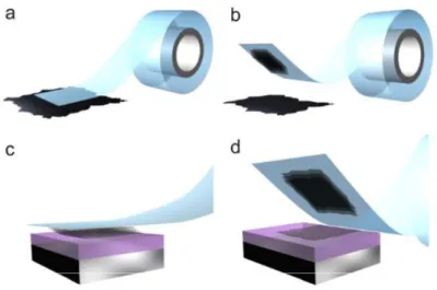
on the different synthesis methods among 15 000 representative selected articles taken from Web of Science (accessed 31/01/2020). ... 32 Figure 1. 7 Micromechanical exfoliation of 2D crystals. (a) Adhesive tape is pressed against a 2D crystal so that the top few layers are attached to the tape (b). (c) The tape with crystals of layered material is pressed against a surface of choice. (d) Upon peeling off, the bottom layer is left on the substrate87. ... 33
Figure 1. 8 Growth mechanism of graphene sheets on different types of metal catalysts. (a) Inhomogeneous multilayer graphene tends to grow on Ni and Co, which has high C solubility. (b) Uniform single-layer graphene can be grown on low C solubility metal, like Cu92. ... 34
Figure 1. 9 Growth of epitaxial graphene on silicon carbide wafer via sublimation of silicon atoms95. ... 35
Figure 1. 10 A Liquid-phase exfoliation of graphene adapted from106. ... 36
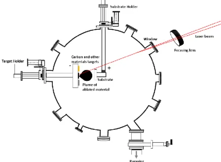
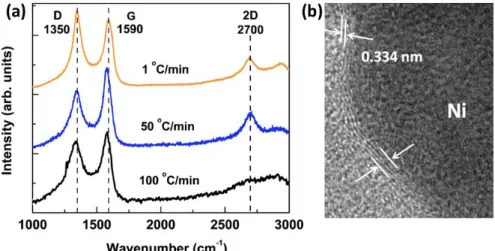
Figure 1. 11 Synthesis of graphene using various PVD methods: deposition of amorphous carbon using PVD and transformation into graphene by thermal annealing. ... 37 Figure 1. 12 Schematic of the illustration of the pulsed laser deposition technique. ... 40 Figure 1. 13 A schematic description of the different steps for PLD graphene synthesis using a metallic catalyst thin film. ... 42 Figure 1. 14 (a) Raman spectra of samples cooled at different rates (b) Cross-section TEM showing at the graphene layers above Ni adapted from ref132. ... 47
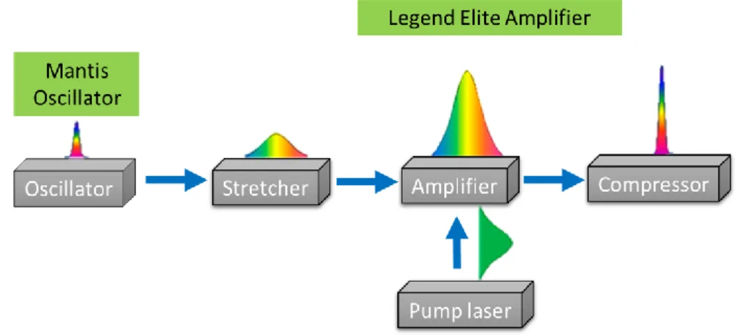
Figure 1. 15 Energy dispersion of graphene around the Dirac point, indicating a change in the Fermi level. Blue indicates levels filled with electrons while orange indicates empty levels. (a) Undoped graphene. (b) Nitrogen-doped graphene (n-type). (c) Boron-doped graphene (p-type). ... 49 Figure 2. 1 (a) Schematic illustration of pulsed laser deposition vacuum chamber, (b) Photo of the used vacuum chamber machine. ... 66 Figure 2. 2 Schematic of chirped pulse amplification (CPA) of the femtosecond laser system. ... 67 Figure 2. 3 The optical assembly of the KrF excimer laser ... 67 Figure 2. 4 Radial distribution of the laser fluence ... 68
9
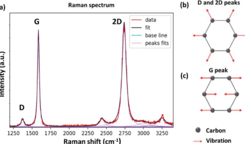
Figure 2. 5 Linear regression performed on the surfaces of ablation craters. The target is made of silicon and each crater is obtained from 10 shots. ... 69 Figure 2. 6 A schematic illustration of the synthesis of nitrogen-doped graphene film from amorphous carbon nitride (a-C: N). ... 71 Figure 2. 7 A schematic illustration of pulsed laser co-deposition (PLD) of carbon and boron (a-C:B), and its conversion into boron-doped graphene via thermal treatment. ... 72 Figure 2. 8 SEM image of the cross-section of boron film used to calibrate the ablation rate on Si substrate. ... 72 Figure 2. 9 (a) Photograph of AS-One 100 furnace, fabricated by Annealsys; (b) Schematic illustration of Rapid Thermal Annealing RTA system. ... 75 Figure 2. 10 (a) Photograph of DektakXT stylus profilometer from our lab (b) Schematic of a stylus profilometer. ... 77 Figure 2. 11 Schematic of a Raman spectrometer ... 77 Figure 2. 12 (a) Raman spectrum from our synthesized graphene with the three major characteristic peaks. (b) Representation of the vibrational mode related to D and 2D peak. (c) Representation of the vibrational mode associated with the G peak. ... 78 Figure 2. 13 (a) Raman spectra of ABA and ABC trilayer graphene; (b) Optical image and (c) corresponding spatial map of the spectral width of the Raman 2D‐mode feature for trilayer graphene samples25. ... 81
Figure 2. 14 (a) Scheme of the XPS process, showing photoionization of an atom by the ejection of a 1s electron. ... 83 Figure 2. 15 (a) Schematic of the signals resulting from the interaction of the electrons with the sample in SEM analysis. (b) The excitation volume for the generation of each signal. ... 85 Figure 2. 16 (a) A typical cyclic voltammetry potential. (b) Voltammogram of the reversible reduction of a 1 mM Fc+ solution to Fc, at a scan rate of 100 mV s−150. ... 89 Figure 3. 1 The synthesis process of N-doped graphene films, by thermal heating of a Ni/a-C:N/SiO2 with in situ XPS analysis. ... 96 Figure 3. 2 SEM images of a) the as-deposited Ni/a-C:N/SiO2 before annealing b) after annealing at 300 °C and c) after annealing at 500 °C performed in the ultrahigh vacuum in the XPS chamber. Electron backscattering diffraction (EBSD) orientation map along the sample’s Z-direction of d) sample annealed at 300°C and e) 500°C2. ... 98
Figure 3. 3 N1s peak recorded at the end of the annealing treatment at 500 °C before cooling2.
... 100 Figure 3. 4 XPS analysis of C1s at the end of annealing treatments with adjustments of C1 peaks using the four components: a) at 200 °C; b) at 300 °C ... 100 Figure 3. 5 Angle-resolved XPS analysis of C1s at the end of annealing treatment at 500 °C before cooling: a) adjustments of C1 peaks at two photoelectron escape angles using the four components, b) relative depth plot based on the logarithm of the ratio of intensities at ϴ=35° and ϴ=65°, and indicating the relative sensitivity to the surface of each component used to adjust C1s, c) Schematic in-depth distribution based on the relative depth plot results of the carbon species: graphene weakly interacting with Ni “component CGr”, graphene strongly interacting with Ni “component CB”, carbide “component Ccarbide” and carbon dissolved “component Cdis”2. ... 101
Figure 3. 6 a) Raman spectra of the N-doped graphene films after heat treatments at 300 °C and 500 °C in an ultrahigh vacuum; b) Raman mappings (10 x 10 µm²) of the I2D/IG and ID/IG intensity ratios related to the N-doped graphene film synthesized at 500°C. The white mark corresponds to the location of the spectrum depicted in (a). The values 0.30 and 0.23 correspond to the mean values of the I2D/IG and ID/IG intensity ratios respectively over the mapped area; c) Raman characteristics deduced from the spectra depicted in Figure a and b. ... 102
10
Figure 3. 7 Changes in the function of the square root of the time of surface sensitive components CGr and CB of C1s core level expressed as a fraction of the monolayer using Eq.3.2 and bulk sensitive components Ccarbide and Cdis expressed in atomic percent units using Eq.3.3.2
... 105 Figure 3. 8 a ratio of the fraction of the CGr to the CB component as a function of dissolved carbon based on the kinetics data at 200, 300 and 500 °C (Figures 3.7 a, b and d). The sketches a,b,c, and d indicate the effect of C dissolved on the growth of graphene strongly catalyst interacting with nickel (purple) and weakly catalyst interacting graphene layer (purple) for the ranges delimited by dotted lines2. ... 107
Figure 3. 9 Schematic illustration of the diffusion-segregation model used to fit the experimental kinetics measured using XPS. Ci is considered constant over time at a given temperature (Dirichlet boundary condition). Meshing: one hundred slices in the 150 nm nickel film. ... 109 Figure 3. 10 (a) Surface segregation kinetics of carbon during annealing at 200, 300 and 500 °C using the bulk diffusion coefficient of carbon in nickel; (b) Time dependence of dissolved carbon concentration just below the segregated layer during annealing at 200, 300 and 500 °C using the bulk diffusion coefficient of carbon in nickel; (c) Surface segregation kinetics of carbon during annealing at 200 and 300 °C using an accelerated diffusion coefficient of carbon in nickel; (b) Time dependence of dissolved carbon concentration just below the segregated layer during annealing at 200 and 300 °C using an accelerated diffusion coefficient of carbon in nickel. ... 112 Figure 4. 1 Description of the three parts of this chapter: section I: substrate effect on graphene growth, choice of deposition sequence, and annealing condition. Section II: influence of the thickness of amorphous carbon on the graphene growth. Section III: impact of the nickel catalyst thickness on graphene synthesis. ... 118 Figure 4. 2 Synthesis route of graphene obtained by combining pulsed laser deposition and rapid thermal annealing on both Si(100) and SiO2 substrates. The formation of nickel silicides with the Si(100) substrate is detailed in the following paragraphs. ... 119 Figure 4. 3 (a) ID/IG and La Raman mapping of as-grown graphene at temperatures ranging from 600-1000°C on Si(100) with their mean values, (b) ID/IG and La Raman mapping of as-grown graphene at temperatures ranging from 600-1000°C on SiO2 with their mean values. ... 121 Figure 4. 4 Plots showing dependence on growth temperature as a function of the average value of ID/IG ratio, crystallite size (La), I2D/IG ratio and the FWHM (2D) for the synthesized graphene: (a) on Si (100); (b) on SiO2. ... 122 Figure 4. 5 I2D/IG and 2D (FWHM) Raman mapping of as-grown graphene at temperatures ranging from 600-1000°C, with their average values (a) on Si (100), (b) on SiO2. ... 122 Figure 4. 6 Typical experimental (black) and fitted (blue) Raman spectra of the synthesized graphene films at temperatures ranging from 600-1000°C: (a) on Si (100), (b) on SiO2 (the red insert corresponds to the deconvolution of the 2D peak of the spectrum of graphene at 1000°C on SiO2). ... 123 Figure 4. 7 (a) Histogram of the I2D/IG intensity ratio measured by Raman spectroscopy of 400 graphene films of (a) G-Si-600 sample, (b) G-SiO2-1000 sample. ... 124 Figure 4. 8 Raman spectra at 633 nm for as-grown graphene with various growth temperatures from 600 to 1000°C (a) On Si(100) substrate, (b) On SiO2 substrate. ... 125 Figure 4. 9 (a) D, G, and 2D positions Raman mapping of as-grown graphene at temperatures ranging from 600-1000°C, with their average values (a) on Si (100), (b) on SiO2. ... 126 Figure 4. 10 D, G, and 2D peak positions depending on growth temperature for graphene grown (a) on Si(100), (b) on SiO2. ... 127 Figure 4. 11 (a) Raman mapping of I2D/IG and ID/IG ratios over 20 × 20 μm² region for the
11
synthesized graphene using Ni/a-C stacking order. (b) Raman mapping of I2D/IG and ID/IG ratios over 20 × 20 μm² region for the synthesized graphene using a-C/Ni stacking order. (c) Extracted Raman spectra of the graphene in both Raman mapping. ... 130 Figure 4. 12 (a) Raman mapping of I2D/IG and ID/IG ratios over 20 × 20 μm² region for the synthesized graphene using a-C/Ni deposition order with 60 nm of Ni and annealing conditions (Condition 1: 900°C, 10 min, 15°C/s and -1°C/s). (b) Raman mapping of I2D/IG and ID/IG ratios over 20 × 20 μm² region for the synthesized graphene using a-C/Ni deposition order with 50 nm of Ni and annealing conditions (Condition 2: 900°C, 7 min, 15°C/s and -0.5°C/s). (c) Extracted typical Raman spectra of the graphene in both Raman mapping (black circle). ... 131 Figure 4. 13 (a) Raman spectroscopy maps of I2D/IG of all samples; (b) plot of the influence of the initial a-C thickness on the average I2D/IG values as a function of growth temperature. . 134 Figure 4. 14 (a) Raman spectroscopy maps of ID/IG of all samples; (b) plot of the influence of the initial a-C thickness on the average ID/IG values as a function of growth temperature. ... 135 Figure 4. 15 Raman mapping statistics: 3D plot of percentage graphene layer number distribution as a function of the initial a-C thickness (top) and the coverage percentage values (bottom). (a) 800 °C; (b) 900 °C; (c) 1000 °C. ... 136 Figure 4. 16 Raman mapping of a large 100 ×100 μm² region, of sample a-C (2 nm – 900 °C): (a) Mapping of I2D/IG ratio with an average value of 1.06; (b) Mapping of ID/IG ratio with the average value of 0.12; (c) spectra of the graphene with different numbers of layers in Raman mapping of graphene on a SiO2 substrate; (d) Statistical histogram of the Raman mapping of I2D/IG ratio showing the predominance of bilayer; (e) Fitting of the 2D band in the Raman spectrum of bilayer graphene showing an asymmetric shape and four Lorentzian peaks corresponding to AB stacking; (f) table showing the other Raman mapping parameters of the sample. ... 137 Figure 4. 17 AFM and SEM images of sample a-C (2 nm – 900 °C): (a) SEM image after graphene synthesis showing different contrast and the nickel residual nodules; (b) SEM image after nickel removal with FeCl3 treatment. Inset shows the EDS spectrum indicating the absence of Ni; (c) AFM image after graphene growth showing the surface morphology with a RMS value of 182 nm; (d) AFM image after nickel removal showing the surface morphology with lower roughness RMS value of 61 nm. ... 138 Figure 4. 18 XPS spectra of sample a-C (2 nm – 900 °C) before FeCl3 treatment: (a) XPS survey spectrum; (b) XPS C 1s spectrum; (c) XPS O 1s spectrum32. ... 139
Figure 4. 19 (a) Transmittance curves as a function of wavelength for both: as-deposited sample (bottom) and the synthesized bilayer graphene after thermal annealing and FeCl3 etching and the blank fused silica (top). (b) Raman mapping of I2D/IG ratio of the bilayer graphene after Ni etching, (c) an extracted spectrum from the mapping depicting the bilayer graphene feature. ... 140 Figure 4. 20 Synthesis route for A) rapid thermal annealing of Ni thin films and B) free-transfer graphene films obtained by pulsed laser deposition of carbon on Ni thin films followed by rapid thermal annealing and Ni etching. The substrate is SiO2 in both cases. ... 142 Figure 4. 21 Summary of the solid-state dewetting behavior for nickel thin films deposited on fused silica SiO2 substrate: SEM images of the dewetting of the nickel thin film of 25 nm (a-e), 50 nm (f-j) and 150 nm (k-o), as a function of annealing temperature (500-900°C range). The three stages related to the Ni dewetting mechanism, described in the text, are superimposed on the SEM images. ... 143 Figure 4. 22 Particle size distribution corresponding to the 3rd stage of the Ni dewetting process, obtained by using ImageJ software on the SEM images in Fig.2, and related to the 25 nm thick Ni film after thermal annealing at 700, 800 and 900°C, and the 50 nm thick Ni film after thermal annealing at 900°C. ... 146 Figure 4. 23 Comparison of the solid-state dewetting behavior for nickel thin films deposited
12
on fused silica SiO2 substrate in the presence and absence of graphene at 900°C. (a-c) SEM images of the dewetting of nickel thin film of 25, 50, and 150 nm at 900°C in absence of carbon. (d-f) SEM images of the dewetting of nickel thin film of 25, 50, and 150 nm at 900°C in presence of carbon. (g) Histogram of particle size distribution extracted from the SEM image in Figure 4.23d. (h) Histogram of particle size distribution extracted from the SEM image in Figure 4.23e. The insets in both figures are the values of the mean perimeter, surface coverage, and interparticle spacing of the nickel particles. ... 147 Figure 4. 24 Raman analysis of the synthesized graphene using 25 nm thick of nickel catalyst : (a) Raman mapping of ID/IG ratio in a 20 ×20 μm² region with the average value of 0.25 ; (b) Raman mapping of I2D/IG ratio in a 20 ×20 μm² region with the average value of 0.62; (c) A representative spectrum from the mapping of the synthesized graphene, its position corresponds to the white mark in the Raman mappings ; (d) Statistical histogram of the Raman mapping of I2D/IG ratio showing the few-layer predominance. ... 150 Figure 4. 25 (a) SEM image of the as-synthesized graphene using the 25 nm thick of nickel catalyst, after annealing at 900°C; (b) EDS spectra of two different regions of the samples, the grey-black zone (on the top) and the white islands zone (below); (c) SEM image of the treated graphene with FeCl3 for nickel particles removal leading to the appearing of the interfacial graphene; (d) EDS spectra of two different regions of the samples, the zone with traces of islands (on the top) and the grey-black zone (below), both showing the absence of nickel; (e) Raman mapping of I2D/IG ratio in a 20 ×20 μm² region with an average value of 0.58 of the interfacial graphene after FeCl3 treatment. The inset shows a representative spectrum from the Raman mapping; (f) HRTEM image of resulting graphene edges showing five layers, after FeCl3 treatment. The inset is the intensity profile image. ... 151 Figure 4. 26 Raman analysis of the as-synthesized graphene using 50 nm of nickel catalyst film: (a) Raman mapping of ID/IG ratio in a 20 ×20 μm² region with the average value of 0.26; (b) Raman mapping of I2D/IG ratio in a 20 ×20 μm² region with the average value of 1.08; (c) Statistical histogram of the Raman mapping of I2D/IG ratio showing the bilayer graphene predominance. (d) Representative spectra from the mapping of the as-grown graphene, their positions are highlighted with the corresponding number of the layer in the Raman mappings. ... 152 Figure 4. 27 (a) SEM image of the as-synthesized graphene using the 50 nm of nickel catalyst film. (b) EDS spectra of two different regions of the samples, the white islands zone (on the top) and the grey-black zone (below). (c) SEM image of the treated graphene with FeCl3 for nickel particles removal leading to the appearing of the interfacial graphene (d) EDS spectra of two different regions of the samples, the zone with traces of islands (on the top), and the grey-black zone (below), both showed the absence of nickel. (e) Raman mapping of I2D/IG ratio in a 20 ×20 μm² region with the average value of 0.91 of the treated graphene with FeCl3. The inset shows a bilayer graphene spectrum from the Raman mapping of the Fecl3 treated graphene. (f) HRTEM of resulting graphene edges from 50 nm of nickel, showing two layers after FeCl3 treatment. The inset is the intensity profile image. (g – h) HRTEM of resulting graphene from 50 nm of nickel, showing a “one monolayer” area (red circle) and the hexagonal atomic resolution of the monolayer graphene. The purple dots in the inset of Figure. 4.27h highlights the hexagonal structure of graphene. ... 153 Figure 4. 28 (a) SEM image of the as-synthesized graphene using the 150 nm of nickel catalyst film, showing a dark and bright contrast for thicker and thinner graphene respectively. (b) EDS spectra of two different regions of the samples, the grey-black zone (on the left) and the white islands zone (right). (c) Representative spectra from the sample of the as-grown graphene, their positions are illustrated with the corresponding number of the layer in the Raman mapping. (d) Raman mapping results of G peak intensity with the sample area of 20 ×20 μm². (e) Raman mapping results of 2D peak intensity with the sample area of 20 ×20 μm². ... 155
13
Figure 4. 29 A schematic illustration of graphene growth at the top surface of nickel film and in the interface between the Ni and SiO2 substrate along with the nickel dewetting process. (a) The stage with carbon diffusion and segregation through nickel for the initial graphene formation before the start of the nickel dewetting (low temperature, e.g. 500°C) (b) The stage related to the beginning of the nickel dewetting (c) The stage with the end of nickel dewetting process. During stages (b) and (c), the initially formed graphene undergoes certainly further evolution in terms of nanostructures. ... 157 Figure 4. 30 Transmittance curve as a function of wavelength for both: derived graphene from 25 nm nickel (bottom) and the synthesized graphene derived from 50 nm nickel (top) (middle) after thermal annealing and FeCl3 etching and the blank fused silica (top). The inset at the bottom figure shows the appearance of both samples after graphene growth and Ni etching. ... 159 Figure 4. 31 Description of the different sections of this chapter, the conditions colored in red are those used for obtaining our best free transfer continuous graphene. ... 160 Figure 5. 1 The synthesis process of B-doped graphene films, by PLD and thermal heating of an a-C:B/Ni SiO2(300nm)/Si. ... 169 Figure 5. 2 (a) XPS-B1s, (b) XPS-C1s spectrum, (c) XPS-O1s spectrum. All of a-C:B (9 at.%). ... 171 Figure 5. 3 High resolution XPS spectra of BG (2.5 at.%): (a) C1s, (b) B1s, (c) O1s. High-resolution XPS spectra of BG (1 at. %): (d) C1s, (e) B1s, (f) O1s. ... 172 Figure 5. 4 ID/IG, I2D/IG, 2D (FWHM), La, G, and 2D positions Raman mappings of (a) undoped graphene, (b) boron-doped graphene 1%, (c) boron-doped graphene 2.5%, with their average values. ... 173 Figure 5. 5 Plots showing the dependence on boron doping level as a function of the average value of (a) ID/IG ratio, I2D/IG ratio, (b) crystallite size (La), the FWHM (2D), and (c) G and 2D peaks positions for the synthesized undoped and boron-doped graphene (1, 2.5 at%). (d) Typical experimental (black) and fitted (blue) Raman spectra of the synthesized undoped and boron-doped graphene films (1, 2.5 at.%). ... 174 Figure 5. 6 Cyclic voltammetry curves measured in a 0.5 M 1, 1’ ferrocene-dimethanol solution of 0.1 M NaClO4 with the scan rate of 50 mV/s. (a) CV of undoped graphene. (b) CV of BG1%. (c) CV of BG2.5%. (d) All the CV curves together. ... 176 Figure 5. 7 Plot of Ψ against ν-1/2 enabling the estimation of the kinetic rate of interfacial electron transfer constant ko. ... 178 Figure 5. 8 Cyclic voltammetry on BG20 in a 0.5 M 1, 1’ferrocene-dimethanol solution of 0.1 M NaClO4 (a) for 0 min (red), 5 min (blue), 10 min (green), and 30 min (black); (b) for 0 min (red) and 24 hours (purple). The scan rate is 50 mV/s. ... 179 Figure 5. 9 The correlation between the kinetic rate of interfacial electron transfer (ko) and the average intensity ratio of the D-peak over the G-peak (ID/IG) of the G, BG1% and BG2.5%. ... 180
14
List of Tables
Table 1. 1 The most exceptional properties of single-layer graphene compared to other materials such as ITO (Indium-Tin Oxide), FTO (Fluorine-doped Tin Oxide), Silicon, Copper, carbon
nanotubes, and steel. ... 29
Table 1. 2 Summary of graphene grown on different substrates using PLD method without a metallic catalyst layer ... 43
Table 1. 3 Summary of graphene grown on different substrates using the PLD method with a metallic catalyst layer ... 46
Table 2. 1 Carbon, nitrogenated amorphous carbon, boron deposition rate as a function of the used fluences. ... 70
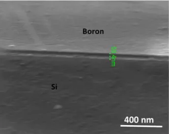
Table 2. 2 Parameters of the elaboration of boron-doped amorphous carbon using the co-ablation of carbon and boron. ... 74
Table 2. 3 Summary of all the investigation techniques used in this thesis and relating accessible results. ... 76
Table 2. 4 Summary of I2D/IG ratio used for the estimation of the graphene layer number in this thesis. ... 80
Table 3. 1 Experimental conditions for thermal heating of Ni/a-C:N/SiO2 films, with in situ XPS during heating and ex-situ complementary experiments. ... 97
Table 4. 1 The samples and their growth conditions. RTA annealing was performed in a low vacuum at 5×10⁻² mbar for 600 s, preceded by a +15°C/s heating ramp and followed by cooling limited to -1°C/s. ... 120
Table 4. 2 Average values and their standard deviations of the Raman characteristics resulting from the 400 Raman spectra performed on representative areas of the synthesized graphene and presented as Raman mappings in the following paragraphs. ... 120
Table 4. 3 Summary of the conditions of graphene synthesis. ... 132
Table 4. 4 Summary of the average values of each I2D/IG and ID/IG maps respectively. ... 133
Table 4. 5 Summary of growth conditions. ... 142
Table 4. 6 Summary of the statistical values of the average perimeter, surface coverage, and interspacing of nickel particles extracted from the SEM images in Figure 4.21 and Figure 4.23. ... 145
Table 4. 7 Summary of the different characteristics of the resulting graphene from the synthesis process using 25, 50, and 150 nm thick of nickel film. ... 156
Table 5. 1 Average values and their standard deviations of the Raman characteristics resulting from the 400 Raman spectra performed on representative areas of the synthesized undoped and boron graphene. ... 173
Table 5. 2 Results of electrochemical measurements on BG and undoped graphene films... 176
Table 5. 3 Results of electrochemical measurements on BG2.5% for a different time duration in ferrocene dimethanol with the scan rate of 50 mV/s. ... 179
15
Résumé de la thèse en français
Le graphène est, par définition, un matériau bidimensionnel, cristallin, constitué d’un réseau d’atomes de carbone en nid d’abeilles répartis sur une monocouche atomique. Le graphène est la « brique élémentaire » du graphite. Cependant, une évolution sémantique dans la communauté scientifique ne limite pas seulement le terme « graphène » à une monocouche de carbone, mais jusqu'à une dizaine de couches1, ce qui représente une épaisseur de l’ordre de 3
à 4 nanomètres. En outre, de nos jours, la littérature scientifique utilise le terme « graphène et matériaux associés » (Graphene and Related Materials) pour dénommer toute variante de ce matériau élaboré par divers procédés de synthèse2.
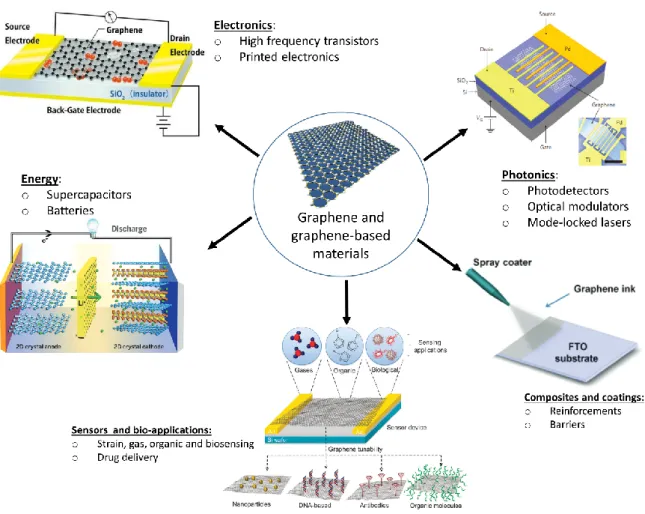
Le graphène a suscité un grand intérêt dans les communautés scientifiques au cours des 15 dernières années, en raison de propriétés remarquables, en particulier la conductivité électrique, la transparence optique, la résistance et la conductivité thermique, avec de nombreuses applications technologiques potentielles, comme les électrodes transparentes, l’émission de champs, les biocapteurs, les futures générations de batteries, les matériaux composites, etc. Les recherches sur le graphène constituent l’exemple même des programmes les plus récents des travaux contemporains sur les matériaux à base de carbone, aux échelles micrométrique et nanométrique, si l'on considère les travaux antérieurs sur d’autres matériaux carbonés comme le Diamond-Like Carbon (DLC), les nanotubes de carbone (CNT) et les fullerènes.
La recherche sur le graphène a pris son essor avec les travaux pionniers de Geim et Novoselov en 2004, travaux qui ont conduit à l’attribution du prix Nobel de physique en 2010. Ce fut le point de départ d'une production scientifique colossale à l’échelle internationale, comme nous l’évoquerons dans notre bibliographie, production basée sur des programmes scientifiques et technologiques ambitieux dans de nombreux pays et continents, comme le Flagship Européen sur le graphène actuellement en cours. Aujourd'hui, après 15 ans de recherches intensives, les communautés scientifiques et industrielles cherchent à consolider et fiabiliser les méthodes de synthèse du graphène pour mieux comprendre les relations entre synthèse et propriétés, et produire des couches de graphène de qualité reproductible sur de grandes surfaces selon les standards de la microélectronique. Dans un article récent, Reiss et al.2 ont observé que 124 ans
séparent la découverte de silicium en 1824 et la première puce de silicium en 1958, et de nos jours la production de puces à base de silicium est une activité industrielle de masse. Le
16
graphène nécessitera-t-il une période de gestation aussi longue? Probablement pas, si l'on considère les moyens scientifiques et techniques mobilisés actuellement sur ce sujet. Cependant, prêtons attention à une affirmation des auteurs de l’article de Reiss et al.2 : « Mettre
un nouveau matériau sur le marché n'est pas sans défi et, de nos jours, les gens semblent penser que le développement de matériaux peut être aussi rapide que les développements de logiciels, ce qui n'est clairement pas le cas. Les innovations basées sur de nouveaux matériaux sont difficiles, longues et coûteuses, et souvent elles ne se concrétisent pas » (De Réf.2, traduit de l’anglais). La « réussite » du graphène n’est donc pas encore un acquis !
En conséquence, le plus grand défi, avec le graphène, demeure le contrôle et la reproductibilité de la synthèse sur de grandes surfaces, ainsi que l'étude analytique, à l’échelle nanométrique, de films si particuliers à une échelle très réduite, films constitués de l’élément carbone formant une ou plusieurs couches déposées (ou transférées) sur des substrats adéquats en fonction des applications visées. Les scientifiques engagés dans la recherche sur les matériaux à base de graphène, soulignent à l'unanimité le besoin impérieux de valider la fiabilité et la reproductibilité des procédés, en explorant méticuleusement les relations nanostructure - propriétés macroscopiques non sans lien avec le procédé d’élaboration.
Ces recherches constituent un immense défi dans l’étude des matériaux en ce début du 21ème siècle. L'objectif de cette thèse est d’apporter une contribution à ces efforts déployés sur le long terme à l’échelle internationale. Nous avons choisi une approche particulière pour réaliser la synthèse du graphène, le dépôt par ablation laser pulsée (Pulsed Laser Deposition), qui permet en particulier le dopage des couches de graphène par des atomes choisis, de manière contrôlée et reproductible. En effet, par dopage, il est possible de modifier à la demande les propriétés intrinsèques du graphène. Ainsi, le graphène dopé peut présenter des propriétés intéressantes dans les domaines de l’électronique et du magnétisme, ou encore en chimie et électrochimie. Un large éventail d'applications utilisant des matériaux à base de graphène dopés est attendu. Différents types de dopants peuvent être introduits dans le graphène, tels que l’azote, le bore, le phosphore, le soufre, et bien d’autres encore, comme nous le détaillerons dans notre étude bibliographique.
À ce jour, le dépôt chimique en phase vapeur (Chemical Vapor Deposition) apparaît comme la méthode la plus étudiée et la plus prometteuse pour la synthèse du graphène. Cette méthode est déjà bien développée dans les laboratoires et commence à être utilisée dans l’industrie pour la production du graphène. Cependant, elle nécessite une étape à haute température (environ 1000°C), une source de carbone gazeux et un processus de transfert des couches de graphène
17
sur le substrat choisi, ce qui reste souvent problématique. En matière de dopage, se posent des difficultés récurrentes de contrôler la concentration en dopants dans le graphène, à partir des phases gazeuses précurseurs.
Dans cette thèse, nous proposons une méthode de synthèse alternative basée sur un procédé physique (et non chimique), combinant le dépôt par laser pulsé (PLD) avec un recuit thermique rapide (Rapid Thermal Annealing). La PLD est bien connue pour réaliser le dépôt d’un précurseur de carbone solide, et cette méthode est maîtrisée par notre laboratoire depuis une vingtaine d’années, notamment pour la synthèse de DLC et de DLC dopés. Quant au RTA, il est utilisé pour un chauffage rapide qui permet d'obtenir du graphène à partir du précurseur élaboré par PLD, avec la possibilité d’éviter le processus de transfert. Les températures de chauffage peuvent être significativement inférieures à celles utilisées en CVD. La PLD consiste à vaporiser, grâce à la lumière focalisée d'un laser, une cible généralement constituée du matériau que l'on veut obtenir sous forme de film mince. Le matériau est ablaté sour la forme d’un panache constitué d’un plasma, et déposé sur le substrat choisi. Le procédé PLD permet souvent le dépôt d'un matériau de stœchiométrie quasi identique à celle de la cible, et la co-ablation ou l'co-ablation en présence d'un gaz réactif permet le contrôle de la composition d’un film multi-élémentaire, donc en particulier dopé.
Les objectifs scientifiques de la présente thèse sont donc d'étudier la croissance du graphène et du graphène dopé au bore en utilisant le procédé de synthèse par PLD combiné au traitement thermique par RTA. Nous étudierons l’effet de plusieurs paramètres sur la nature des films de graphène obtenus. L'incorporation de bore dans le graphène vise à apporter de nouvelles fonctionnalités au graphène. Nous chercherons à comprendre le mécanisme de croissance du graphène et du graphène dopé au bore, synthétisés en présence d’un catalyseur métallique. Nous caractériserons les films de graphène purs et dopés, pour mieux comprendre l'influence du procédé sur leurs nanostructures et leurs compositions. Enfin, nous explorerons les propriétés électrochimiques des films de graphène pur et de graphène dopé au bore, pour esquisser une perspective d’applications de ces films.
Même si cette thèse n'est pas le premier travail sur le graphène, elle ouvre une voie physique originale pour la synthèse et le dopage du graphène d'une manière contrôlable et probablement plus versatile que d’autres méthodes d’élaboration. Nos travaux cherchent à élargir les champs d'études de la PLD dans le domaine de la synthèse des couches minces. Ils contribuent à une avancée des connaissances fondamentales sur la synthèse du graphène et du graphène dopé au
18
bore, au cœur des efforts actuels de la recherche pour intégrer ces matériaux dans des applications technologiques exigeants des performances toujours plus élevées.
Ce manuscrit de thèse se structure en cinq chapitres.
Le Chapitre 1 propose une synthèse bibliographique sur notre sujet. Cette synthèse se veut assez brève sur le graphène, déjà largement présenté dans des revues de synthèse. Nous insisterons davantage sur l’élaboration du graphène par le procédé PLD.
Le Chapitre 2 présente la méthodologie expérimentale que nous avons mise en œuvre dans nos recherches. Cette méthodologie concerne d’une part le procédé d’ablation laser pulsé couplé au traitement thermique RTA pour la synthèse du graphène et du graphène dopé, d’autre part les méthodes de caractérisation complémentaires afin de sonder, selon une approche multi-échelle, la nanoarchitecture, la composition et les propriétés électrochimiques des films élaborés. Le Chapitre 3 présente les mécanismes de croissance du graphène à partir d’une couche mince amorphe à base de carbone, élaborée par PLD. La méthode originale que nous avons utilisée est une analyse chimique par spectroscopie de photoélectrons X (XPS) mise en œuvre in situ pendant le chauffage sous vide, et donc pendant la croissance du graphène. Nous avons mis en évidence un mécanisme de diffusion – ségrégation du carbone dans le catalyseur métallique à base de nickel. Nous avons montré que la croissance du graphène débute à des températures relativement basses (300°C) et se poursuite au moins jusqu’à 500°C. Un modèle de diffusion – ségrégation a été mis en œuvre pour mieux comprendre les mécanismes observés expérimentalement.
Le Chapitre 4 explore l’effet des paramètres de synthèse a priori les plus influents sur la nature et la nanoarchitecture des couches de graphène obtenus, en termes de nombre de couches, de défauts, de tailles des amas de carbone graphéniques et d’homogénéité en surface. Nous démontrons plus particulièrement les effets de la nature des substrats à base de silicium, de l’épaisseur initiale de la couche de carbone et de la couche du catalyseur métallique, et des paramètres du traitement thermique RTA, notamment la température. Aux températures les plus élevées, nous mettons en évidence un phénomène, déjà connu, de démouillage du catalyseur métallique, bien en-deçà de son point de fusion. Nous avons cherché à mettre en évidence quels pouvaient être les liens entre ce démouillage (qui dépend de la température et de l’épaisseur du film catalytique) sur la qualité du graphène obtenu. Ces travaux nous ont permis de cerner une gamme de paramètres (épaisseur de la couche carbonée précurseure, épaisseur du catalyseur,
19
température RTA) permettant d’optimiser les couches de graphène. Une perspective de production de graphène sans procédé de transfert ultérieur est ainsi ouverte.
Le chapitre 5 propose, sans doute pour la première fois à notre connaissance dans la littérature scientifique, la synthèse de graphène dopé au bore, par couplage de la PLD avec le RTA. Nous mettons en évidence qu’il est envisageable de contrôler la teneur en bore dans le graphène, en contrôlant cette teneur dans la couche précurseure réalisée par co-ablation de carbone et de bore, et ce même si cette concentration est affectée par le traitement RTA. Enfin, nous avons exploré le comportement électrochimique des couches de graphène dopé au bore, comparées aux couches de graphène non dopé. Ces travaux, très préliminaires et conduits en fin de thèse, mettent en évidence un effet significatif du dopage au bore sur la cinétique électrochimique observée.
La conclusion permet une synthèse de l’ensemble, et dessine quelques perspectives scientifiques pour la suite de ces travaux de recherche.
Références
1. Ye, R. & Tour, J. M. Graphene at Fifteen. ACS Nano (2019) doi:10.1021/acsnano.9b06778. 2. Reiss, T., Hjelt, K. & Ferrari, A. C. Graphene is on track to deliver on its promises. Nat.
20
General Introduction
Graphene is, by definition, a one-atom-thick pure carbon crystal with a honeycomb-like structure. However, a semantic evolution in the scientific community does not only limit the term “graphene” to a carbon monolayer but up to 10 layers1. Besides, nowadays, the literature
uses the term “Graphene and related materials (GRM)” to name any variant of this wonder material2. Graphene has become of great interest in both scientific and engineering communities
from the past 15 years, owing to its range of unique properties including high conductivity, transparency, strength, and thermal conductivity, with many potential applications in research and industry, as transparent electrodes, field emitters, biosensors, batteries, composites, and so on. The research on graphene constitutes one of the most recent and contemporary stages of investigation in the scientific community of carbon-based at the micrometer and nanometer scales if one considers the literature dealing typically on Diamond-Like Carbon (DLC) films, carbon nanotubes (CNT), fullerenes.
Research on graphene has emerged with the pioneering work of Geim and Novoselov in 2004 and their Nobel Prize in Physics in 2010. This was the “starting point” of a huge worldwide scientific production, as mentioned later in our first chapter, based on ambitious scientific and technological programs in many countries and continents, as the European Flagship on Graphene presently in progress. Nowadays, about 15 years after the “graphene take-off”, the scientific and industrial communities are looking to consolidate the synthesis methods of graphene to better understand and control the correlation between synthesis and properties. In a recent paper, Reiss et al.2 observed that 124 years separate the discovery of silicon in 1824,
and the first silicon chip in 1958, and now Si chip production is a mass-market activity. Does graphene require such a similarly long period? Probably not, if one considers the scientific and technical means mobilized today. However, let us mention an assertion written by the already mentioned authors:
“Bringing a new material to market is not without its challenge and, in this day and age, people seem to assume that materials development can be as quick as software developments, which is clearly not the case. Innovations based on new materials are hard, long, and expensive, and often it does not come to final fruition” (From Ref.2).
As a consequence, the highest challenge, with graphene, remains the control and reproducibility of the synthesis over wide surfaces, as well as the analytical investigation at (ultra) low scales,
21
of films constituted by a light element (carbon) forming one or few-layer deposited (or transferred) on adequate substrates depending on the targeted applications. Therefore, scientists committed in graphene-based material research, emphasize unanimously the strong need to provide trusted validation on graphene related-materials, meaning to explore meticulously the nanostructure – macroscopic property relationships, in connection with the synthesis route. This is a great challenge, and the objective of this Ph.D. project is to contribute to this long-term work in progress, by considering a particular approach to achieve the graphene synthesis, including doping of graphene layers in a controlled and reproducible way. Indeed, by doping, it is possible to modify on demand the intrinsic properties of graphene. Thus, doped graphene presents interesting properties such as superconductivity, ferromagnetism, and enhanced chemical and electrochemical activity, which promote a wide range of applications using graphene-based materials. Various types of dopants have been introduced in graphene material such as N, B, P, or S, as mentioned later in our bibliography.
To date, chemical vapor deposition (CVD) appears the most promising route of graphene synthesis, and this method is already well developed in both the laboratory and industry environments. However, it requires high-temperature treatment, gas carbon source, and a transfer process, which is still problematic. In this Ph.D. project, we propose an alternative synthesis method, combining pulsed laser deposition (PLD) with rapid thermal annealing (RTA). On one side, PLD allows the deposition of the solid carbon precursor, and on the other side, RTA is used for rapid heating which makes it possible to obtain graphene without the need for transfer. PLD consists of vaporizing, thanks to the focused light of a laser, a target generally made up of the material that one wants to obtain in the form of a thin film. The material is ejected into a plasma ablation plume and is deposited on a substrate. The PLD process generally allows the deposition of a material of the same stoichiometry as the target, and co-ablation or ablation in the presence of a reactive gas allows control of the film composition. The scope of the present thesis is therefore to study the growth of graphene and boron-doped graphene by using the PLD method combined with the RTA process. Indeed, the incorporation of boron aims to bring new graphene functionality.
Firstly, we aim to understand the mechanism of PLD graphene growth. Secondly, the goal is to synthesize and characterize pure and doped graphene films to better understand the influence of the process on their structures and properties. Lastly, we started to explore the electrochemical performance of pure graphene and boron-doped graphene films, to provide a perspective of applications of such films. Even though this thesis is not the first work on graphene, it paves a new physical route for graphene synthesis and doping in a controllable
22
manner, which appears to be much easier compared to the other methods. It widens the investigation fields of PLD in the field of thin-film synthesis. It also pushes a little further scientific knowledge to consolidate the graphene topic, which is at a critical time in its existence compared to the expected applications.
This Ph.D. project was performed in Laboratoire Hubert Curien of University Jean Monnet (Saint-Etienne, France), in the frame of GRAPHENE project, labeled by LABEX MANUTECH SISE (Surface and Interfaces Science and Engineering) of Université de Lyon, a consortium of academic laboratories and industries supported by the French “Plan d’Investissements d’Avenir”. Our investigations were supported by the research theme “Laser-matter interaction” of Laboratoire Hubert Curien, focused on laser irradiation effects in condensed matter for material processing, functionalization, and fabrication. We also relied on the experimental tools and skills of four platforms of Laboratoire Hubert Curien: “Ultra-short laser”, “Planar Technology and Instrumentation”, “Characterization” and “Electron microscopy”. Indeed, this work enabled access to different characterization spectroscopy and microscopy techniques: Raman spectroscopy, Scanning Electronic Microscopy, Atomic Force Microscopy, and Transmission Electron Microscopy were performed at Laboratoire Hubert-Curien. Transmission electron microscopy was carried out by Yaya Lefkir and Stéphanie Reynaud. X-Ray Photoelectron spectroscopies were performed either at Ecole Nationale Supérieure des Mines de Saint-Etienne (Vincent Barnier), at Synchrotron SOLEIL (José Avila) and Ecole Centrale de Lyon (Jules Galipaud), depending on the availability of the apparatus. We also worked on a model of carbon diffusion developed by Frédéric Christien at Ecole Nationale supérieure des Mines de Saint-Etienne. For electrochemical analysis, a collaboration was made with Institut des Sciences Analytiques (ISA) of Lyon (Carole Farre and Carole Chaix) for cyclic voltammetry measurements on our undoped and boron-doped graphene.
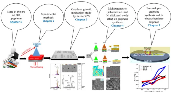
This manuscript is organized in five chapters as illustrated in Figure 0.1 and outlined below. In Chapter 1, we discuss the graphene generalities and review the state of the art about the growth of graphene using the pulsed laser deposition method. By doing so, we realized that PLD has been less extensively used for graphene and doped graphene synthesis, which had encouraged our work.
In Chapter 2, we describe the experimental protocols related to the synthesis method and the characterization techniques including microscopies (SEM, AFM, and HRTEM), spectroscopies (Raman, XPS, UV-Visible absorption) and cyclic voltammetry for electrochemical property measurement.
23
Chapter 3 is devoted to the study of the PLD graphene growth mechanism by carbon diffusion-segregation through the nickel catalyst. Herein, we demonstrated, using thermal heating performed with in situ XPS, how carbon starts to diffuse through nickel at relatively low temperatures, and segregates into graphene sheets on the top surface, at a temperature well below temperatures required in CVD processes to achieve graphene. Thanks to a model of diffusion-segregation, we were able to discuss the graphene synthesis mechanism from a solid carbon source obtained by PLD.
Figure 0. 1 Illustration of the organization of the contents of this Ph.D. manuscript.
Chapter 4 reports the multi-parametric studies for the optimization of PLD graphene synthesis. With this study, we observed that silicon-based substrates used for graphene growth highly influence the quality and layer number of the resulting graphene, whether it is silicon or fused silica. Moreover, the starting thicknesses of the amorphous carbon and the nickel catalyst, as well as annealing temperature, affect considerably the synthesized graphene.
Chapter 5 concerns the boron doping effects in terms of structural, chemical, and electrochemical properties of graphene. Here, we successfully demonstrated for the first time the use of the PLD method for synthesis of boron-doped graphene exhibiting an electrochemical performance much higher than the one of undoped graphene. All these results position the pulsed laser deposition method as an alternative route for graphene and doped graphene synthesis.
Finally, we summarized our main results in the general conclusions, paving the way towards future research suggestions.
24
References
1. Ye, R. & Tour, J. M. Graphene at Fifteen. ACS Nano (2019) doi:10.1021/acsnano.9b06778. 2. Reiss, T., Hjelt, K. & Ferrari, A. C. Graphene is on track to deliver on its promises. Nat.
25
Chapter 1: Graphene synthesis using pulsed laser
deposition: State of art
I.
Background on graphene
Graphene is an exceptional two-dimensional (2D) material that has a significant interest in both academia and industry research. The first study on graphene, or 2D graphite, can be dated to as early as 1947 when Wallace examined the electronic energy bands in crystalline graphite using the ‘tight binding’ approximation1. Since it was shown that the semi-metallic phase is unstable
in two dimensions (2D)2, single-layer graphene has long been regarded as ‘academic’ material.
Even so, many experimental efforts were made to obtain single-layer graphene. For example, in 1992, the single-layer graphite structure produced by hydrocarbon decomposition was observed on the Pt(111) surface under a scanning tunneling microscope (STM)3. In 1997,
Ohashi and co-workers4 cleaved graphite material to evaluate the thickness impact of graphite
crystals on electrical properties. They reduced with success the thickness of graphite films to 30 nm. In 2004, Novoselov and Geim5 inspired by the previous works presented a reliable
approach for making single-layer graphene by repeatedly peeling highly oriented pyrolytic graphite (HOPG). This demonstration of the mechanical exfoliation technique, known as the scotch tape method, caused a good sensation and excited several research groups to analyze the structure and properties of graphene. Consequently, Geim and Novoselov awarded the Nobel Prize in Physics 2010 for their innovative experiments on graphene material. Graphene structure presents a 2D honeycomb lattice, with a compact single layer of carbon atoms. Being the basic block for all graphitic materials, the graphene plane can be wrapped into 0D fullerenes, rolled into 1D nanotubes, or stacked into 3D graphite6,7 as shown in Figure 1.1.
1. Graphene crystalline structure
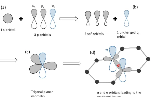
The word “graphene” is made up of the prefix “graph” from graphite and the suffix “ene” from the carbon/carbon double bonds8. Graphene is a two-dimension (2D) form of graphite, in other
words, graphene can be called 2D graphite. The electronic structure of carbon is composed of 6 electrons including 4 of valence: 1s² 2s² 2p², which gives rise to an s orbital and three p (px, py, pz) orbitals presenting sp² or sp3 hybridizations depending on the structure. Sp3 hybridization gives rise to four covalent bonds (this is the case of diamond or Diamond-Like Carbon (DLC)). In the case of graphene, but also fullerenes (C60), carbon nanotubes, and graphite, sp²
26
hybridization between the s orbital and two p (px and py) orbitals lead to a trigonal planar structure with the formation of three covalent in-plane σ-bonds (Figure 1.2). These covalent σ bonds between carbon atoms form the hexagonal structure of graphene with an interatomic length of ~ 0.142 nm and are responsible for its good mechanical strength. The additional pz orbital perpendicular to the planar structure of graphene occupies the out-of-plane π bond. The overlap of the pz between neighboring carbon atoms gives rise to the formation of the π half-filled bond, responsible for the electronic conductivity of graphene.
Figure 1. 1 Illustration of graphene as a mother of carbon allotropes and can be converted to fullerenes, carbon nanotubes, and graphite. Adapted from reference7.
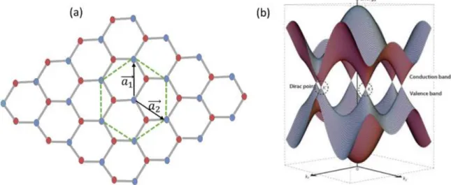
The structure of graphene is composed of a unit cell of two carbon atoms. It consists of two triangular sublattices with two non-equivalent atoms illustrated by the blue and orange atoms in Figure 1.3a. The interatomic distance of two atoms is a0 = 0.142 nm and the lattice vectors can be described as:
𝑎1 = a
2(1, √3) , 𝑎2 = a
2(1, −√3) Where a = 0.246 nm is the lattice constant in the plane.
27
Figure 1. 2 Illustration of the carbon sp2 hybridization: (a) its electronic structure comprises an s orbital
and three p orbitals. (b) The sp2 hybridization consists of three sp2 orbitals and one p
z orbital
perpendicular to the other three, (c) triangular planar geometry, (d) π, and σ orbitals leading to the graphene lattice.
The velocity of delocalized electrons in graphene is constant and independent of momentum, which leads to the conclusion that the charge carriers (electrons and holes) can be described by the Dirac equation for the massless particles with an effective speed of light vF = 106m/s. The band structure of graphene presented in Figure 1.3b is different from metal and is different from the semiconductor band structure because there is no energy gap. For this reason, graphene can be considered a zero bandgap material. The band structure of graphene is positioned somewhere around these two extremes, which make graphene to act like a semimetal. In a closer look at Figure 1.3b, it can be observed that the valence and conduction bands meet at the Fermi energy, forming conical bands, which touch at the K and K’ high-symmetry points in the Brillouin zone. The absence of an electronic bandgap in graphene limits its applicability in various areas such as transistors technology where a bandgap is needed for on-off switching operations. However, the bandgap of graphene can be tuned by electrical or chemical doping. This is why graphene doping has emerged as a hot topic in the past few years. The discussion about the chemical graphene doping with nitrogen and boron will be detailed further in this chapter.
The term “graphene” is often prefixed by “monolayer or single layer,” “bilayer,” “trilayer,” “few-layer” or “multilayer.” To address the discrepancy in definitions, the International
28
Organization for Standardization (ISO) released its chosen terminologies for graphene and graphene derivatives in 2017. It defines the layer numbers of graphene as the following: single-layer graphene (SLG), bisingle-layer graphene (BLG), and few-single-layer graphene (FLG) to be 1, 2, and 3−10, respectively9. This definition was based on the finding that SLG is a semimetal with zero
bandgap5,and its stacking changes the physical and electronic properties8,10.
Figure 1. 3 (a) Graphene lattice representation: the two inequivalent atoms of the unit cell are highlighted with blue and red colors. (b) Graphene energy bands close to the Fermi level: the conduction and valence bands touch at K and K’ points. Adapted from11.
In terms of the stacking order, single-layer graphene (SLG) does not have stacking but can exist in a rippled form. The bilayer (BLG) and few-layer (FLG) graphene can display different stacking arrangements, as illustrated in Figure 1.4. These stacking orders include mainly the Bernal stacking (AB)12, the rhombohedral stacking (ABC)13, and turbostratic stacking with an
interlayer spacing > 0.342 nm larger than that of crystalline graphene (0.335 nm)14.
Figure 1. 4 Schematic stacking order for trilayer graphene with (a) Bernal or ABA stacking and (b) Rhombohedral or ABC stacking order.
The turbostratic stacking is a specific lattice arrangement with no discernible stacking order and exhibits relative rotational angles that cannot be described by the classic atomic plane