HAL Id: tel-00595906
https://tel.archives-ouvertes.fr/tel-00595906
Submitted on 25 May 2011
HAL is a multi-disciplinary open access archive for the deposit and dissemination of sci-entific research documents, whether they are pub-lished or not. The documents may come from teaching and research institutions in France or abroad, or from public or private research centers.
L’archive ouverte pluridisciplinaire HAL, est destinée au dépôt et à la diffusion de documents scientifiques de niveau recherche, publiés ou non, émanant des établissements d’enseignement et de recherche français ou étrangers, des laboratoires publics ou privés.
EXPERIMENTAL STUDY ON THE SPIN-ORBIT
COUPLING PROPERTY IN LOW-DIMENSIONAL
SEMICONDUCTOR STRUCTURES
Hongming Zhao
To cite this version:
Hongming Zhao. EXPERIMENTAL STUDY ON THE SPIN-ORBIT COUPLING PROPERTY IN LOW-DIMENSIONAL SEMICONDUCTOR STRUCTURES. Condensed Matter [cond-mat]. Univer-sité de Grenoble, 2010. English. �tel-00595906�
UNIVERSITE DE GRENOBLE
THÈSE
présentée par
Hongming ZHAO
pour obtenir le grade de
Docteur de l’Université de Grenoble
Spécialité: NANOPHYSIQUE
DANS LE CADRE D’UNE COTUTELLE
Institute of Physics, Chinese Academy of Sciences (CAS) –
CHINE
Arrêtés ministériels: 6 janvier 2005 – 7 août 2006
ETUDE EXPERIMENTALE DE LA PROPRIETE DE
COUPLAGE SPIN-ORBITE DANS DES STRUCTURES
SEMI-CONDUCTRICES DE BASSE DIMENSIONALITE
Soutenue le 19 juillet 2010
Thèse dirigée par les Professeurs Kuntheak KHENG et Dongmin CHEN
JURY:
M. Xavier MARIE
Rapporteur
M. Yang JI
Rapporteur
M. Dongmin CHEN
Examinateur
M. Kuntheak KHENG
Examinateur
Équipe mixte Nanophysique et Semiconducteurs
Instistut Néel/CNRS et Institut Nanoscience et Cryogénie (INAC)/CEA-Grenoble et
Solid State Quantum Information and Quantum Computation Laboratory
Experimental Study on the Spin-Orbit Coupling Property in Low-dimensional Semiconductor Structures
UNIVERSITE DE GRENOBLE
THÈSE
présentée par
Hongming ZHAO
pour obtenir le grade de
Docteur de l’Université de Grenoble
Spécialité: NANOPHYSIQUE
DANS LE CADRE D’UNE COTUTELLE
Institute of Physics, Chinese Academy of Sciences (CAS) –
CHINE
Arrêtés ministériels: 6 janvier 2005 – 7 août 2006
EXPERIMENTAL STUDY ON THE SPIN-ORBIT
COUPLING PROPERTY IN LOW-DIMENSIONAL
SEMICONDUCTOR STRUCTURES
19 July 2010
Thèse dirigée par les Professeurs Kuntheak KHENG et Dongmin CHEN
JURY:
M. Xavier MARIE
Rapporteur
M. Yang JI
Rapporteur
M. Dongmin CHEN
Examinateur
M. Kuntheak KHENG
Examinateur
Équipe mixte Nanophysique et Semiconducteurs
Instistut Néel/CNRS et Institut Nanoscience et Cryogénie (INAC)/CEA-Grenoble et
Solid State Quantum Information and Quantum Computation Laboratory
Experimental Study on the Spin-Orbit Coupling Property in Low-dimensional Semiconductor Structures
Acknowledgments
Acknowledgments
I would like to express my heartfelt gratitude to Professor Kuntheak KHENG, my supervisor in France, for his proposition of this research project and guidance. The research project could not have obtained its present results without his consistent and illuminating instruction.
I would like to thank Professor Dongmin CHEN who is my supervisor in China sincerely for his constant encouragement and support. His instruction led me into the world of experimental physics.
I am also greatly indebted to my associate supervisor in China, Professor Baoli LIU, for his intellectual suggestions and helpful discussions.
This joint educational program would not have been possible without the assistance of Professor Joël CIBERT, Professor Henri MARIETTE, and Professor Xavier. MARIE. I would like to express my heartfelt gratitude to them.
I also would like to thank Dr. Joël BLEUSE for the critical assistance and discussions. My special thanks go to Dr Laurent LOMBEZ and Dr. Adrien TRIBU for their care and all of their helpful suggestions. I could always go to them whenever I had a problem.
Many thanks to my friends, both in China and in France. I shall always cherish the happy memories of our delightful friends.
Finally, I reserve my deepest gratitude to Miss Shanshan WANG who is my girlfriend and my family for their constant love and support.
Experimental Study on the Spin-Orbit Coupling Property in Low-dimensional Semiconductor Structures
Table of Content
Table of Content
Abstract ··· I
Structure of the Thesis ··· V
Published Papers related to the Thesis ··· XI 1. Electron density dependence of in-plane spin relaxation anisotropy in GaAs/AlGaAs
two-dimensional electron gas (Chapter 6 of the thesis) ··· XIII 2. Experimental observation of isotropic in-plane spin splitting in GaN/AlGaN
two-dimensional electron gas (Chapter 7 of the thesis) ··· XV 3. Electron spin quantum beats and room temperature g factor in GaAsN
(Chapter 8 of the thesis) ··· XVII 4. Optical characterization of type-II CdTe/CdSe/CdTe heterostructure nanorods
(Chapter 9 of the thesis) ··· XIX 5. Optical Analysis of a series of Size and Shape-controlled Type-II CdTe/CdSe/CdTe
Heterostructure Nanorods (Chapter 9 of the thesis) ··· XXI
Publications ··· XXIII
Thesis (Chinese) ··· XXV
Chapter 1: Introduction ··· 1
Chapter 2: Overview of Semiconductor Spintronics ··· 7
Chapter 3: Introduction of Semiconductor Spectroscopy and Dynamics of Carriers ··· 27
Chapter 4: Overview of Spectroscopy Experimental Technique ··· 41
Chapter 5: Construction of Ultrafast Optical Laboratory ··· 53
Chapter 6: Experimental Study on the in-plane Spin Relaxation Anisotropy in (001) GaAs/AlGaAs Two-Dimensional Electron Gas ··· 71
Experimental Study on the Spin-Orbit Coupling Property in Low-dimensional Semiconductor Structures
II
Chapter 7: Experimental Observation of Isotropic in-plane Spin Splitting in GaN/AlGaN Two-Dimensional Electron Gas ··· 87 Chapter 8: Experimental Study on Electron Spin Quantum Beats and Room Temperature g factor in GaAsN ··· 99 Chapter 9: Experimental Research of Optical Characterization of Type-II
CdTe/CdSe/CdTe Heterostructure Nanorods ··· 109 Chapter 10: Summary of the Thesis ··· 125
Résumé en français ··· XXVII
Abstract
I
Abstract
In the past few decades, with the rapid development of semiconductor physics and technology, microelectronic devices have become smaller in size. Based on the Moore’s Law, which summarized the growth of microelectronics, the scientists and engineers are inevitably faced with the limit of quantum mechanics as the size of individual bits approaches nanoscale. For this reason, physicists have been eager to exploit the quantum mechanical property of electron in semiconductor electronic devices: the spin, which is a purely quantum phenomenon.
Spintronics (Spin + Electronics) is a multidisciplinary field which aims to develop a new kind of spintronic devices to replace the traditional electronic devices and has achieved much progress the last decade. With the development of reserach in spintronics, the spin degree of freedom is studied widely in magneto-electronic devices, quantum information and quantum computation. Semiconductor structure is one of the most important areas of physics. The semiconductor spintronics, which is a combined subject of the semiconductor structures and spintronics, is not only abundant in physical meaning, but also easy to merge with the most advanced and the most delicate fabricated technology of semiconductor. It would be expected to be the foundation of developing new generation low power dissipation, high speed and highly integrated spintronics devices.
The main purpose of semiconductor spintronics research is to use the electronic spin as the information carrier and using the spin degree of freedom to replace the charge in traditional device. Spin-orbit interaction is important to semiconductor spintronics as it enables spin orientation and detection (optical or electronic method). As a result, an in-depth insight into the spin-orbit coupling (SOC) properties for injecting, probing and controlling of spin in semiconductor is an important content in the research. In this thesis we have systematically studied the SO coupling in low dimensional semiconductor structures by recombination dynamics and spin relaxation process.
Experimental Study on the Spin-Orbit Coupling Property in Low-dimensional Semiconductor Structures
II
Optical spectroscopy is a major experimental technique to unravel, exploit, and control the dynamics of the entity spin in semiconductors. The study of optical properties, especially the ultrafast optical properties, in semiconductors is one of the most hot topic in the semiconductor physics. It covers many important physical processes of carrier excitation, relaxation, transfer and recombination, and greatly speed up the development of the basic science and device application. The short optical laser pulses on the picosecond or femtosecond timescale are the technical basis of most time-resolved optical experiments. In those experimental techniques, Time Resolved Kerr/Faraday Rotation-TRKR/FR system is an effective method to study the spin dynamics and spin relaxation process in semiconductors. We established an ultrafast optical laboratory on the basis of time resolved Kerr/Faraday rotation technique with electronics devices and low temperature-magnet field system to study the optical properties and SO coupling properties in low dimensional semiconductors.
The steady-state photoluminescence (PL) spectra and Time resolved PL (TRPL) spectra experimental techniques are another two important experimental technologies to obtain the properties of carriers and SO coupling in low dimensional semiconductors. In order to extend our contents and field of research, the author of this thesis learned and researched the PL and TRPL experimental system, and investigated the optical characteristic in a series of size and shape-controlled low dimensional semiconductor structures.
The main results are:
The spin dynamics of two-dimensional electrons in (001) GaAs/AlGaAs heterostructure were investigated by the time-resolved Kerr rotation (TRKR) technique under a transverse magnetic field. The in-plane spin lifetime is found to be anisotropic below 150 K due to the interference of Rashba and Dresselhaus spin-orbit coupling and D’yakonov-Perel spin relaxation. The ratio of in-plane spin lifetimes is measured directly as a function of temperature and pump power, showing that the
Abstract
III electron density in two-dimensional electron gas channel strongly affects the Rashba spin-orbit coupling. Refer to Applied Physics Letters 90, 112111 (2007). Then, the large anisotropy of the magnitude of in-plane g factor for conduction electrons in asymmetric (001) GaAs/AlGaAs quantum well and the tendency of temperature dependence were studied by Larmor beats observed by TRKR under a transverse magnetic field.
The first experimental study of the in-plane-orientation dependent spin splitting in the C(0001)-oriented GaN/AlGaN two-dimensional electron gas at room temperature was reported. Both the short spin relaxation time (τs =14ps), obtained from TRKR, and the marked circular photogalvanic effect (CPGE) current induced by the inter-band transition give clear evidence of a sizeable spin splitting in this system. By monitoring the CPGE current, the experiment clearly shows the isotropic in-plane spin splitting in this system for the first time. Most of the optical spin orientation work has been concentrated in narrow-band gap such as GaAs systems. This work makes a new contribution to the understanding of the SOC in wide band gap low-dimensional structure. Refer to Applied Physics Letters 91, 252105 (2007).
For the research project of GaAsN materials, our work is the first experimental measurement of conduction electron Landé g factor in dilute nitrides semiconductor compounds at room temperature using time-resolved Kerr Rotation technique. It demonstrates that the conduction electron Landé g factor can be modified drastically by introducing a small amounts of nitrogen in GaAs bulk. This work enhances our understanding on the spin and magneto-optical properties of GaNAs with a small nitrogen fraction. Refer to Applied Physics Letters 95, 041911 (2009).
The optical characteristic of indirect type II transition in a series of size and shape-controlled linear CdTe/CdSe/CdTe heterostructure nanorods was studied by steady-state photoluminescence (PL) spectra and Time resolved PL (TRPL) spectra. The energy and lifetime of the photoluminescence from charge-separated band structure can be tuned by the nature of nanorods’ band edges. Our results show the
Experimental Study on the Spin-Orbit Coupling Property in Low-dimensional Semiconductor Structures
IV
size-dependent transfer from type I direct transition (CdSe~600nm) to the indirect type II transition (CdSe/CdTe). The suitable size of heterostructure nanorod for charge separation (no type-I recombination) was obtained. A long PL decay time which is more than 1000 nanosecond and increases with PL wavelength has been found in indirect type II transition at 5K, which can be rationalized by the changing of wavefunction overlap of electrons and holes induced by the quantum confinement effect in type-II band structure. Refer to “Optical characterization of type-II CdTe/CdSe/CdTe heterostructure nanorods”, Journal of Physics: Conference Series, 210, 012029, (2010) and the paper for Quantum Dot 2010. Further experiments and theoretical analysis about the decay dynamics in this system and the relationships among PL intensities and decay time are currently underway.
Keywords: Spintronics, Spin-Orbit Coupling, Semiconductor Structure, Quantum Well, Two-Dimensional Electron Gas, Semiconductor Spectroscopy, Time-Resolved Kerr Rotation
Structure of the Thesis
V
Structure of the Thesis
The treatise concerns Introduction, text and epilogue. There are ten chapters from which the first four ones bear a preparatory character. The comprehensive introduction of research background (chapter 1 and chapter 2), theory of semiconductor spectroscopy (chapter 3), experimental technique (chapter 4), and the construction of laboratory (chapter 5) are given. The core of the thesis consists of chapters corresponding to published or accepted manuscripts (chapter 6, 7, 8 and 9).
The main contents are as following: Chapter 1: Introduction
This chapter dwells on the research background, the significance of the topic, the frame and new points of the thesis.
Chapter 2: Overview of Semiconductor Spintronics
This chapter is about the history and evolution of spintronics, the significance and application of semiconductor spintronics, and the experiment method (spin generation/injection, transport, manipulation and detection) of semiconductor spintronics. The spin relaxation mechanism in semiconductors is a key point. These mechanisms include the Elliott-Yafet mechanism, the D’yakonov-Perel’ mechanism, the Bir-Aronov-Pikus mechanism, and the spin dephasing induced by the hyperfine interaction. In the research of this thesis, the spin relaxation mechanism dominates at room temperature is the D’yakonov-Perel’ (DP) mechanism.
Chapter 3: Introduction of Semiconductor Spectroscopy and Dynamics of Carriers
This chapter expounds the theory related to the thesis. These include the theory of semiconductor spectroscopy, the optical spin orientation in semiconductors, dynamics of carriers and the optical properties of low-dimensional semiconductor structures.
Experimental Study on the Spin-Orbit Coupling Property in Low-dimensional Semiconductor Structures
VI
Chapter 4: Overview of Spectroscopy Experimental Technique
This chapter is about the experimental equipments and methods of steady-state photoluminescence, time resolved photoluminescence and time-resolved Kerr/Faraday rotation technique.
Chapter 5: Construction of Ultrafast Optical Laboratory
Introduction to the construction process and the solution method of key technology problem of the ultrafast optical laboratory which is in Institute of Physics/Beijing National Laboratory for Condensed Matter Physics, Chinese Academy of Sciences. The laboratory is on the basis of time resolved Kerr/Faraday rotation technique with electronics devices and low temperature-magnet field system. In addition, the micro-fabrication process and technology of the devices used in experiments are given. These include: UV lithography, etching, thermal evaporation and so on.
Chapter 6: Experimental Study on the in-plane Spin Relaxation Anisotropy in (001) GaAs/AlGaAs Two-Dimensional Electron Gas
The spin dynamics of two-dimensional electrons in (001) GaAs/AlGaAs heterostructure was investigated by the time-resolved Kerr rotation (TRKR) technique under a transverse magnetic field. The in-plane spin lifetime is found to be anisotropic below 150 K due to the interference of Rashba [J. Phys. C 17, 6039 (1984)] and Dresselhaus [Phys. Rev. 100, 580 (1955)] spin-orbit coupling and D’yakonov-Perel [Sov. Phys. Solid State 13, 3023 (1972)] spin relaxation. The ratio of in-plane spin lifetimes is measured directly as a function of temperature and pump power, showing that the electron density in two-dimensional electron gas channel strongly affects the Rashba spin-orbit coupling. The results of the study were published in “Electron density dependence of in-plane spin relaxation anisotropy in
Structure of the Thesis
VII GaAs/AlGaAs two-dimensional electron gas”, APPLIED PHYSICS LETTERS 90, 112111 (2007).
Then, a large anisotropy of the magnitude of in-plane g factor for conduction electrons in asymmetric (001) GaAs/AlGaAs quantum well from Larmor beats was observed by TRKR technique under a transverse magnetic field. Measurements as a function of temperature reveal the tendency of temperature dependence of in-plane g factor is similar to that reported about the bulk GaAs so far. The observed in-plane g factors also show large anisotropy in the plane of the quantum well in low temperature and strong anisotropic temperature dependence. The off-diagonal element |gxy| (|gyx|) of the g factor tensor, which is the character of in-plane anisotropy, decreases from 0.02128 to nearly 0 as the temperature increase from 10 K to 300 K. We present as well results on the temperature dependence of in-plane anisotropy of spin relaxation time which also agrees well with reported results. Based upon the theoretical prediction [Jetp Letters 57 : 571 (1993)], the in-plane anisotropy comes from the spin-orbit coupling in the semiconductor system with low symmetry C2V and without an inversion center. The variation of the in-plane anisotropy with temperature indicates that the enhanced scattering of electron in higher temperature will effectively weaken the spin-orbit coupling in such system.
Chapter 7: Experimental Observation of Isotropic in-plane Spin Splitting in GaN/AlGaN Two-Dimensional Electron Gas
The circular photogalvanic effect (CPGE) was used to study the in-plane-orientation dependent spin splitting in the C(0001)-oriented GaN/AlGaN two-dimensional electron gas (2DEG). The experiment of monitoring the CPGE current induced by the interband transition clearly shows an isotropic in-plane spin splitting in this system at room temperature for the first time. The spin relaxation time is found to be τs =14ps using the time resolved Kerr rotation technique, which is another evidence of the spin splitting in this 2DEG system.
Experimental Study on the Spin-Orbit Coupling Property in Low-dimensional Semiconductor Structures
VIII
The results of the study were published in “Experimental observation of isotropic in-plane spin splitting in GaN/AlGaN two-dimensional electron gas”, APPLIED PHYSICS LETTERS 91, 252105 (2007)
Chapter 8: Experimental Study on Electron Spin Quantum Beats and Room Temperature g factor in GaAsN
The electron spin quantum beats at room temperature in GaAsN thin films was investigated by time-resolved Kerr rotation (TRKR) technique. The measurement of the quantum beats, which originate from the Larmor precession of electron spins in external transverse magnetic field, yields an accurate determination of the conduction electron g factor. We show that the g factor of GaAs1-xNx thin films is significantly changed by the introduction of a small nitrogen fraction. Our work is the first experimental measurement of conduction electron Landé g factor in dilute nitrides semiconductor compounds at room temperature obtained by TRKR.
The results of the study were published in “Electron spin quantum beats and room temperature g factor in GaAsN”, APPLIED PHYSICS LETTERS 95, 041911 (2009).
Chapter 9: Experimental Research of Optical Characterization of Type-II CdTe/CdSe/CdTe Heterostructure Nanorods
Two series of CdTe/CdSe/CdTe heterostructure nanorods were prepared by the colloidal sequential reactant injection technique. The optical characteristics of an indirect type II transition in these size and shape-controlled nanorods was studied by steady state photoluminescence (PL) and time resolved PL (TRPL) spectra. The energy and lifetime of the PL from the charge-separated band structure can be tuned by the band edges of the nanorods. The results of “core-shell nanorods” show a size-dependent transition from a type I direct transition (CdSe~600 nm) to an indirect type II transition (CdSe/CdTe). The heterostructure nanorod geometry and
Structure of the Thesis
IX dimensions that induce type-II charge separation without type-I recombination were determined. The indirect type II transition at 5 K exhibited a long PL decay time, of more than 1000 nanoseconds, that increased with PL wavelength, which can be rationalized by the changing of wavefunction overlap of electrons and holes induced by the quantum confinement effect in type-II band structure. But the results of “linear nanorods” show different spectral properties, the broad emission peaks (~770nm) in happened all at the same position. The calculations based on the effective mass and envelope function approach to describe the single-particle Hamiltonians will be used to confirm theoretically the interpretations. Then, a discussion about aging effect is made. Due to the aging effect and in order to continue our research, new series of “core-shell nanorods” samples were synthesized. Preliminary results of these new “core-shell nanorods” samples were obtained and discussed in this thesis.
A part of the results were published in “Optical characterization of type-II CdTe/CdSe/CdTe heterostructure nanorods”, JOURNAL OF PHYSICS: Conference Series, 210, 012029 (2010) and “Optical Analysis of a series of Size and Shape-controlled Type-II CdTe/CdSe/CdTe Heterostructure Nanorods” which is the paper accepted by JOURNAL OF PHYSICS: Conference Series, Quantum Dot 2010.
Chapter 10: Summary of the Thesis
In order to study the spin-orbit coupling properties in semiconductors, we established an ultrafast optical laboratory on the basis of time resolved Kerr/Faraday rotation technique with electronics devices and low temperature-magnet field system. We worked out the system integration and achieved a high system sensitivity (1:106). The anisotropy of the in-plane spin lifetimes in the (001)-oriented GaAs/AlGaAs two-dimensional electron gas (2DEG) heterostructure was observed. It exhibits strong electron density dependence. In particular, the Rashba term dominates the Dresselhaus term at higher electron density in the 2DEG sample. These findings could be exploited in future design of spin-related electronic devices.
Experimental Study on the Spin-Orbit Coupling Property in Low-dimensional Semiconductor Structures
X
We have observed the pure CPGE current at interband excitation by polarization-modulated radiation and a short spin relaxation time in wurtzite GaN/AlGaN 2DEG at room temperature. Using the angle dependent measurements of the magnitude of the photocurrent in the plane, we extracted direct information of the isotropic spin splittings in k space in this system for the first time. These results, which are well described by phenomenological theory, should help to shed light on our understanding of the SO coupling in GaN lowdimensional structure.
The accurately the g factor of conduction electrons at RT has been measured in a magnetic field applied perpendicular to the growth axis in GaAs1-xNx films using TRKR technique. We found that the measured g factor changes from 0.28 to 0.22 for x=0.09% to 0.9%. These results demonstrate that the conduction electron Landé g factor can be modified drastically by introducing a small amounts of nitrogen in GaAs bulk.
The optical characterization of a series of linear type-II CdTe/CdSe/CdTe heterostructures nanorods was investigated by steady state PL and TRPL. The size dependent wavelength shift of PL spectra at 5K shows the transfer of charge carries recombination from type-I (CdSe) to type-II transition (CdSe/CdTe) and the competition between the two routes of recombination. In addition, we found the geometric structure which is suitable for the spatial separation of photo-induced charge in CdTe/CdSe system. The weak wavefunction overlap of specially separated electrons and holes was verified by the long lifetime (more than 1000ns) of type-II emission in PL spectra of heterostructures nanorods. Finally, we investigated the emission lifetime at different detected PL wavelength in type-II region. These results can be well explained by the quantum confinement effect in type-II band alignment. Further experiments and theoretical analysis about the decay dynamics in this system and the relationships among PL intensities and PL decay time are currently underway.
Published Papers related to the Thesis
XI
Published Papers related to the Thesis
1. Baoli Liu, Hongming Zhao, Jia Wang, Linsheng Liu, Wenxin Wang, Dongmin Chen, Haijun Zhu. Electron density dependence of in-plane spin relaxation anisotropy in GaAs/AlGaAs two-dimensional electron gas. Appl. Phys. Lett, 90,112111 (2007) [Chapter 6 of the thesis]
2. Hongming Zhao, Baoli Liu, Liwei Guo, Changling Tan, Hong Chen, and Dongmin Chen. Experimental observation of isotropic in-plane spin splitting in GaN/AlGaN two-dimensional electron gas. Appl. Phys. Lett, 91, 252105 (2007) [Chapter 7 of the thesis]
3. H. M. Zhao, L. Lombez, B. L. Liu, B. Q. Sun, Q. K. Xue, D. M. CHen and X. Marie. Electron spin quantum beats and room temperature g factor in GaAsN. Appl. Phys. Lett. 95, 041911 (2009) [Chapter 8 of the thesis]
4. Hongming Zhao, Bonil Koo, Dongmin Chen, Brian A. Korgel and Kuntheak Kheng. Optical characterization of type-II CdTe/CdSe/CdTe heterostructure nanorods. Journal of Physics: Conference Series, 210, 012029. (2010) [Chapter 9 of the thesis]
5. Hongming Zhao, Bonil Koo, J.L. Movilla, Dongmin Chen, Brian A. Korgel and Kuntheak Kheng. Optical Analysis of a series of Size and Shape-controlled Type-II CdTe/CdSe/CdTe Heterostructure Nanorods, accepted by Journal of Physics: Conference Series: Quantum Dot 2010, Nottingham, UK. (2010) [Chapter 9 of the thesis]
Experimental Study on the Spin-Orbit Coupling Property in Low-dimensional Semiconductor Structures
Published Papers related to the Thesis
XIII
1. Electron density dependence of in-plane spin relaxation
anisotropy in GaAs/AlGaAs two-dimensional electron gas
Appl. Phys. Lett, 90,112111 (2007)
Experimental Study on the Spin-Orbit Coupling Property in Low-dimensional Semiconductor Structures
Electron density dependence of in-plane spin relaxation anisotropy in
GaAs/ AlGaAs two-dimensional electron gas
Baoli Liu, Hongming Zhao, Jia Wang, Linsheng Liu, Wenxin Wang, and Dongmin Chena兲
Beijing National Laboratory for Condensed Matter Physics, Institute of Physics, Chinese Academy of Sciences, P.O. Box 603, Beijing 100080, China
Haijun Zhu
Intelligent Epitaxy Technology, Inc., 1250 E. Collins Blvd., Richardson, Texas 70581
共Received 9 January 2007; accepted 7 February 2007; published online 15 March 2007兲
The authors investigated the spin dynamics of two-dimensional electrons in 共001兲 GaAs/AlGaAs heterostructure using the time-resolved Kerr rotation technique under a transverse magnetic field. The in-plane spin lifetime is found to be anisotropic below 150 K due to the interference of Rashba 关J. Phys. C 17, 6039 共1984兲兴 and Dresselhaus 关Phys. Rev. 100, 580 共1955兲兴 spin-orbit coupling and D’yakonov-Perel关Sov. Phys. Solid State 13, 3023 共1972兲兴 spin relaxation. The ratio of in-plane spin lifetimes is measured directly as a function of temperature and pump power, showing that the electron density in two-dimensional electron gas channel strongly affects the Rashba spin-orbit coupling. © 2007 American Institute of Physics.
关DOI:10.1063/1.2713353兴
The ability to manipulate the orientation and the relax-ation of spin populrelax-ation in semiconductor two-dimensional 共2D兲 structures via electrical or optical control is a key step toward building practical spintronics devices.1 In the proto-type device of spin field effect transistor共FET兲, proposed by Datta and Das,2the Rashba spin-orbit共SO兲 coupling3plays a central role in the controlled rotation of spin via external electric field in a two-dimensional electron gas共2DEG兲 sys-tem. In general, the SO coupling includes both Rashba and Dresselhaus4 contributions in a realistic zinc-blende semi-conductor 2D structure, and has the undesired effect of caus-ing spin decoherence in 2DEG at room temperature. The underlying mechanism is the D’yakonov-Perel 共DP兲 spin relaxation,5,6where electron spins randomly precess about an effective magnetic field resulted from the SO coupling and thus dependent on the electron’s momentum.
Recently, methods for controlling the spin relaxation have been proposed for a robust spin FET共Ref. 7兲 and
per-sistent spin helix8 共PSH兲 in 2D structures. The basic idea is to tune the Rashba and the Dresselhaus terms via proper gating or structure engineering, so that they have equal strength in共001兲 2D structures or have only the Dresselhaus term in rectangular共110兲 quantum wells 共QWs兲.9The ability to determine the relative strength of the Rashba and Dressel-haus terms is, therefore, critical to the design of the spin FET and PSH devices. The ratio of Rashba and Dresselhaus terms at a fixed temperature has been measured previously by sev-eral groups.10–12The strengths of both Rashba and Dressel-haus SO coupling also have been investigated by applying a
bias at extreme temperature of approximately
millikelvin.13,14 Theoretically speaking, both Rashba and Dresselhaus terms produce the in-plane effective magnetic field, and the interference of these two terms results in an anisotropic effective magnetic field, and hence an in-plane spin relaxation anisotropy due to DP mechanism.15,16 Thus the anisotropy of in-plane spin lifetimes offers a direct mea-surement of the relative SO coupling strength. In addition,
the nonequilibrium electrons are generated in a 2DEG sys-tem via spin injection during the operation of realistic spin FET and PSH devices, and the change of electron density in a 2DEG system can result in a change of relative SO cou-pling strength. In this letter, we use time-resolved Kerr rota-tion共TRKR兲 technique to study the anisotropic in-plane spin lifetime. We address how the electron density affects the relative strength of the Rashba and Dresselhaus terms via an elevated temperature and/or pump power. We show that the electron density in 2DEG channel will strongly affect the Rashba SO coupling.
The sample studied here consists of GaAs/ AlGaAs het-erostructure grown on a共001兲-oriented semi-insulating GaAs substrate by molecular beam epitaxy. A 500 nm GaAs buffer layer first was grown on the substrate followed by a 14 nm Al0.24Ga0.76As spacer layer, 25 nm Al0.24Ga0.76As Si-doped
4⫻1018cm3, and finally a 1 nm GaAs Si-doping cap layer. The standard Hall measurement gives the electron concentra-tion n = 6.0⫻1011 cm−2 at room temperature, and n = 4.5
⫻1011cm−2at 150 K. We also prepared a GaAs bulk sample
from the same substrate wafer. Two cleaved edges oriented along 关110兴 and 关11¯0兴 axes were prepared for all samples. The TRKR experiment was carried out in an Oxford magneto-optical cryostat supplied with a 7 T split-coil super-conducting magnet. The sample was excited near normal in-cidence with degenerate pump and delayed probe pulses from a Coherent mode-locked Ti:sapphire laser 共⬃120 fs, 76 MHz兲. The center of the photon energy was tuned for the maximum Kerr rotation signal for each sample and tempera-ture setting. The laser beams were focused to a spot size of
⬃100m, and the pump and probe beams have average
power of 5.0 and 0.5 mW, respectively. The helicity of lin-early polarized pump beam was modulated at 50 kHz by a photoelastic modulator for lock-in detection. The circularly polarized pump pulse incident normal to the sample creates spin-polarized electrons with the spin vector along the growth direction of samples. The temporal evolution of the electron spins was recorded by measuring Kerr rotation angle
K共⌬t兲 of the linearly polarized probe pulse while sweeping
a兲Electronic mail: [email protected]
APPLIED PHYSICS LETTERS 90, 112111共2007兲
0003-6951/2007/90共11兲/112111/3/$23.00 90, 112111-1 © 2007 American Institute of Physics
⌬t, which correspond to the net spin component normal to the sample plane.
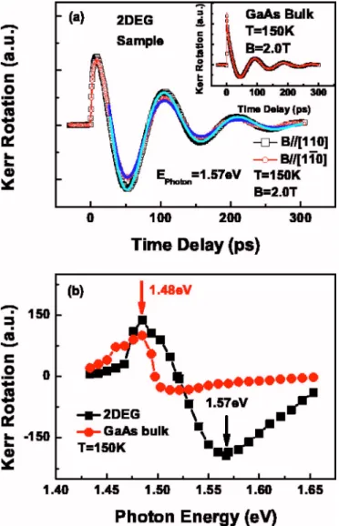
Figure 1共a兲 shows K共⌬t兲 measured at 150 K for a
2DEG sample with an in-plane magnetic field of B = 2.0 T applied along axes 关110兴 and 关11¯0兴, respectively. The data show strong oscillations corresponding to the spin precession with an exponential decay envelope. We found that the am-plitude of oscillation signal of the 2DEG sample with the magnetic field direction along关110兴 was larger than that with magnetic field direction along关11¯0兴. The measured signal of the 2DEG sample may include the contribution of GaAs sub-strate because the photon energy of laser is above the band gap of GaAs bulk. To verify the possible contribution from the GaAs substrate, we measure the spectrum-dependent Kerr rotation signals at 30 ps time delay for both 2DEGs and GaAs bulk samples at the same excitation power with zero magnetic field. As shown in Fig. 1共b兲, the signal of the 2DEG sample reaches the maximum at 1.57 eV photon en-ergy, which is far from the band gap of GaAs at 150 K. It is more than ten times greater than that of pure GaAs bulk sample at this excitation energy. At the photon energy of
1.48 eV, the signal of both 2DEG and GaAs bulk is almost identical. This energy corresponds to the band gap of GaAs bulk at 150 K. Thus by setting the excitation beam at 1.57 eV for our TRKR measurements of the 2DEG sample as shown in Fig. 1共a兲, the effect of GaAs substrate can be safely neglected. Furthermore, we check the TRKR signal at the different sample locations with magnetic field along a fixed direction, for instance, 关110兴 axis. The oscillation sig-nals at all detection positions are essentially the same共data not shown here兲, hence we can exclude possible effect due to sample inhomogeneity in the data reported here. Thus, the data of Fig.1共a兲indicate that the in-plane spin lifetimes are different between spins oriented along关110兴 and 关11¯0兴.
The spin component normal共S⬜兲 to the 2DEG plane can be expressed by17,18
S⬜共⌬t兲 = S0e−共1/⬜+1/储兲⌬t/2cos共gBB⌬t/ប兲, 共1兲
where S0 is a constant,储共⬜兲 is the in-plane 共out-of-plane兲
spin lifetime, g is the electron g factor,B is the Bohr
mag-netron, andប is reduced Planck’s constant. The out-of-plane spin lifetime⬜can be obtained by fitting the experimental data at B = 0 T with a single exponential decay, which is around⬃110 ps at T=150 K. Using this value, and 兩g兩 and储
as fitting parameters, we obtain good fits of Eq. 共1兲 to the data in Fig.1共a兲shown in cyan and blue lines, respectively. While兩g兩=0.36 for both spectra taken with magnetic fields along 关110兴 and 关11¯0兴 axes, the in-plane spin lifetimes are about 30% different; however, for spins oriented along关110兴 and关11¯0兴:储关110兴= 50 ps and储关11¯0兴= 65 ps. Here, we did not
observe the anisotropy of the in-plane electron g factor as reported by Oesreich et al.19 because Rashba term is pre-dominant in共001兲 2DEG heterostructure.13As a control ex-periment, we measured the in-plane spin lifetimes in pure GaAs bulk with magnetic field of B = 2.0 T along关110兴 and 关11¯0兴, respectively, as shown in the inset of Fig.1共a兲. There is no change of signal amplitudes, and the same in-plane spin lifetimes of储= 80 ps are obtained for both applied magnetic
field directions. In bulk GaAs, the spin splitting originates from the Dresselhaus term, which results in an isotropic ef-fective magnetic field. As a consequence, the spin relaxation time in GaAs bulk is isotropic. Thus, the difference in the in-plane spin lifetimes is related to anisotropic in-plane re-laxation in the 2DEG structure.
The above observed anisotropy of the in-plane spin re-laxation can be attributed to the interference of Rashba and Dresselhaus SO coupling in the 2DEG heterostructure.15,16It should be enhanced when the strength of both SO coupling is equal, or reduced when one of the SO coupling terms domi-nates in a 2DEG system. Thus we can use the change of the anisotropy, i.e., the ratio of储关110兴 and储关110兴, to monitor the
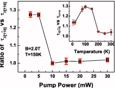
relative change of SO coupling strength. To test this interpre-tation, we tune the relative strength of SO coupling by ma-nipulating the electron density via pump power and/or tem-perature without a gate bias. The advantage of a pure optical control is that the relationship between the SO coupling and the electron density can be obtained without a change of the band structure due to an external electrical field. Figure 2
shows the power dependence of anisotropy with a fixed probe power共0.5 mW兲 under a magnetic field of B=2.0 T and T = 150 K. It is evident that the ratio decreases from 1.3 to 1.0 when the pump power is above 5 mW. This means
FIG. 1.共Color online兲 共a兲 TRKR angleK共⌬t兲 for 2DEG sample measured at a magnetic field of B = 2.0 T and T = 150 K.共b兲 The spectrum-dependent TRKR angle at⌬t=30 ps for both 2DEG and GaAs bulk samples. The black 共red兲 arrow indicates the excitation laser energy for TRKR measurement of 2DEG共GaAs bulk兲 sample. The inset shows the TRKR signal for GaAs bulk sample at B = 2.0 T and T = 150 K.
112111-2 Liu et al. Appl. Phys. Lett. 90, 112111共2007兲
that one of the SO coupling overwhelms the other. At high pump power, only the electron density is changed in 2DEG, which can affect both the Rashba and Dresselhaus SO coupling.13,14 The change of anisotropy in our experiment, however, indicates a different degree of their response to the increasing electron density. Since the Rashba effect is the
main source of spin splitting in 共001兲 2DEG
heterostructure,13 the trend suggests that the higher electron density mainly enhance the strength of Rashba term. We be-lieve that the higher electron density will increase the electric field of confinement potential and hence the strength of Rashba SO coupling is increased as well.
Alternatively, the electron density can be raised at el-evated sample temperature in a 2DEG system, and the DP spin relaxation mechanism dominates in the high tempera-ture regime. The inset of Fig. 2 presents the temperature-dependent anisotropy at a fixed pump power of ⬃5 mW. Initially, the ratio increases from 1.15 to 1.3 with temperature up to 150 K. When the temperature is above 200 K, this ratio drops to 1.0. The electron density at room temperature is larger than that at low temperature in our 2DEG system. This observation further supports that the higher electron density mainly increases the strength of Rashba term. Below 77 K, the ratio is smaller than that in the high temperature regime 共77–150 K兲. This means that other spin relaxation mecha-nisms such as Elliot and Yafet20and Bir, Aronov, and Pikus21
will compete with DP mechanism. Between 77 and 150 K, the DP mechanism dominates. It is consistent with the results obtained in共110兲 QWs.17
In conclusion, we observed an anisotropy of the in-plane spin lifetimes in the 共001兲-oriented GaAs/AlGaAs 2DEG heterostructure, which exhibits strong electron density de-pendence. In particular, the Rashba term dominates the Dresselhaus term at higher electron density in the 2DEG sample. These findings could be exploited in future design of spin-related electronic devices.
This work was supported by the Knowledge Innovation Project of the Chinese Academy of Sciences, the NSFC un-der the Grant No. 10504030, and the Chinese-French PRA Project No. PRA MX06-07.
1Semiconductor Spintronics and Quantum Computation, edited by D. D.
Awschalom, D. Loss, and N. Samarth共Springer, Berlin, 2002兲, Chap. 5.
2S. Datta and B. Das, Appl. Phys. Lett. 56, 665共1990兲. 3Y. A. Bychkov and E. I. Rashba, J. Phys. C 17, 6039共1984兲. 4G. Dresselhaus, Phys. Rev. 100, 580共1955兲.
5M. I. D’yakonov and V. I. Perel, Sov. Phys. Solid State 13, 3023共1972兲. 6Optical Orientation, edited by F. Meier and B. P. Zakharchenya共Elsevier,
Amsterdam, 1984兲, Vol. 8, pp. 11–17.
7J. Schliemann, J. C. Egues, and D. Loss, Phys. Rev. Lett. 90, 146801
共2003兲.
8B. A. Bernevig, J. Orenstein, and S. C. Zhang, Phys. Rev. Lett. 97,
236601共2006兲.
9M. I. D’yakonov and V. Y. Kachorovskii, Sov. Phys. Semicond. 20, 110
共1986兲.
10N. S. Averkiev, L. E. Golub, A. S. Gurevich, V. P. Evtikihiev, V. P.
Kochereshko, A. V. Plotonov, A. S. Shkolik, and Y. P. Efimov, Phys. Rev. B 74, 033305共2006兲.
11C. P. Weber, J. Orienstein, B. A. Bernevig, S. C. Zhang, J. Stephens, and
D. D. Awschalom, Phys. Rev. Lett. 98, 076604共2007兲.
12S. D. Ganichev, V. V. Bel’kov, L. E. Golub, E. L. Ivchenko, P. Schneider,
S. Giglberger, J. Eroms, J. De Boeck, G. Borghs, W. Wegscheider, D. Weiss, and W. Prettl, Phys. Rev. Lett. 92, 256601共2004兲.
13J. P. Lu, J. B. Yau, S. P. Shukla, M. Shayegan, L. Wissinger, U. Rössler,
and R. Winkler, Phys. Rev. Lett. 81, 1282共1998兲.
14T. Koga, J. Nitta, T. Akazaki, and H. Takayanagi, Phys. Rev. Lett. 89,
046801共2002兲.
15N. S. Averkiev and L. E. Golub, Phys. Rev. B 60, 15582共1999兲. 16J. Kainz, U. Rössler, and R. Wrinkler, Phys. Rev. B 68, 075322共2003兲. 17S. Döhrmann, D. Hägele, J. Rudolph, M. Bichler, D. Schuh, and M.
Oestreich, Phys. Rev. Lett. 93, 147405共2004兲.
18K. Morita, H. Sanada, S. Matsuzaka, C. Y. Hu, Y. Ohno, and H. Ohno,
Appl. Phys. Lett. 87, 171905共2005兲.
19M. Oestreich, S. Hallstein, and W. W. Rühle, IEEE J. Sel. Top. Quantum
Electron. 2, 747共1996兲.
20R. J. Elliot, Phys. Rev. 96, 266共1954兲; Y. Yafet, in Solid State Physics,
edited by F. Seitz and D. Turnbull共Academic, New York, 1963兲, Vol. 14, p. 1.
21G. L. Bir, A. G. Aronov, and G. E. Pikus, Sov. Phys. JETP 42, 705
共1976兲. FIG. 2. 共Color online兲 Ratio of in-plane spin lifetimes measured at B
= 2.0 T and T = 150 K vs pump power. Inset: the ratio of in-plane spin life-times measured at B = 2.0 T as a function of temperature.
112111-3 Liu et al. Appl. Phys. Lett. 90, 112111共2007兲
Experimental Study on the Spin-Orbit Coupling Property in Low-dimensional Semiconductor Structures
Published Papers related to the Thesis
XV
2. Experimental observation of isotropic in-plane spin splitting in
GaN/AlGaN two-dimensional electron gas.
Appl. Phys. Lett, 91, 252105 (2007)
Experimental Study on the Spin-Orbit Coupling Property in Low-dimensional Semiconductor Structures
Experimental observation of isotropic in-plane spin splitting in GaN / AlGaN
two-dimensional electron gas
Hongming Zhao, Baoli Liu,a兲Liwei Guo, Changling Tan, Hong Chen, and Dongmin Chenb兲
Beijing National Laboratory for Condensed Matter Physics, Institute of Physics, Chinese Academy of Sciences, P.O. Box 603, Beijing 100080, China
共Received 26 September 2007; accepted 26 November 2007; published online 17 December 2007兲 The circular photogalvanic effect共CPGE兲 was used to study the in-plane-orientation dependent spin splitting in the C共0001兲-oriented GaN/AlGaN two-dimensional electron gas 共2DEG兲. The CPGE current induced by the interband transition shows an isotropic in-plane spin splitting in this system at room temperature. The spin relaxation time is found to be 14 ps using the time resolved Kerr rotation technique, which is another evidence of the spin splitting in this 2DEG system. © 2007
American Institute of Physics. 关DOI:10.1063/1.2824874兴
Spin-orbit 共SO兲 coupling in semiconductor nanostruc-tures has drawn a considerable attention in the field of spintronics.1,2 It offers the physical foundation for electri-cally generating and manipulating spins in conventional semiconductors without the need of magnetic doping,3–7and may lead to practical device applications. While the majority of the work has so far been concentrated on the III-V semi-conductors such as InAs, GaSb, and GaAs, experimental ef-fort has recently begun to shift to the wide band gap materi-als, such as GaN, in which the SO coupling is thought to be weak.8 In GaN/AlGaN heterostructures, spin splitting of 0.1– 9 meV has been observed by magnetoresistance mea-surements and attributed to the SO coupling,9and presence of spin-dependent photocurrent has been tested by the circu-lar photogalvanic effect 共CPGE兲.10 Evidence for the spin Hall effect in InGaN/GaN superlattices has also been reported.11The surprisingly sizable spin splitting of the con-duction band in GaN-based heterostructures mainly results from a large polarization doping effect and a strong interfa-cial electric field directed along the growth axis induced by piezoelectric effect.12–14
In general, the SO coupling in the two-dimensional structures of the III-V semiconductor compounds contains the Rashba and Dresselhaus contributions.8 In a c-axis ori-ented wurtzite-type two-dimensional electron gas 共2DEG兲 structure, both the Rashba and the Dresselhaus terms induce the same electron spin configuration, and the Hamiltonian of the k-linear SO coupling in such systems has the form15
HSO= HD+ HR=␣SO共xky−ykx兲, 共1兲
where␣SO is the spin-orbit coupling constant and equal to
the sum of Rashba and Dresselhaus contributions, x,y are
the in-plane Pauli matrix elements, and kx,y are the in-plane
electron wave vectors. It is clear from Eq.共1兲that the orien-tation of in-plane spins is isotropic and always perpendicular to the direction of the electron motion9 because the system maintains an in-plane inversion symmetry.
The measurement of circular photogalvanic effect, as il-lustrated in Fig. 1共a兲, is a direct way for probing the spin splitting and the in-plane isotropic properties of the spins.16 Using optical interband excitation with the circularly
polar-ized light, one of the spin up and spin down subbands can be nonuniformly populated in k space according to the optical selection rules. This leads to a net spin current adjacent to the point of the incident light. Since the spin relaxation time is short共⬃10 ps兲, the spin current is difficult to be measured directly. However, the relatively long momentum relaxation time will allow these carriers to diffuse a macroscopic dis-tance and can be easily measured.16In the momentum relax-ation time approximrelax-ation, the current induced by the circu-larly polarized light at oblique incidence can be expressed by10,16
j =␥xytptssin0E02Pcircsin/n, 共2兲
where ␥xy is the nonzero component of the second-rank
pseudotensor and is proportional to␣SO, tsand tpare
trans-mission coefficients for linear p and s polarizations given by Fresnel’s formula, and n is the sample index of refraction. E02 and Pcircare the power and helicity of the incident light, and
0and are the polar and azimuthal angles of the light, as
defined in Fig.1共a兲. Since the CPGE current is directly as-sociated with the intrinsic spin splitting in a 2DEG sample, the angular dependent measurements of CPGE current will provide a direct way to measure the isotropy of the in-plane spin splitting in k space. Although the CPGE combined with the linear photogalvanic effect was reported by interband excitation,17attempts to experimentally monitor the isotropic
a兲Electronic mail: [email protected]. b兲Electronic mail: [email protected].
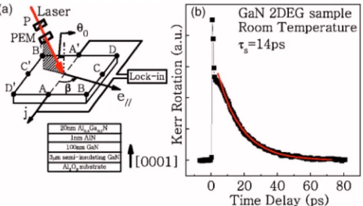
FIG. 1.共Color online兲 共a兲 The simple geometry of the experiment and the structure of the sample. AA⬘, BB⬘, CC⬘, and DD⬘are identification codes of the Ohmic contact pairs, respectively.共b兲 The TRKR angle as a function of delay time on GaN/AlGaN 2DEG sample measured at room temperature. The solid line is the fitting curve.
APPLIED PHYSICS LETTERS 91, 252105共2007兲
0003-6951/2007/91共25兲/252105/3/$23.00 91, 252105-1 © 2007 American Institute of Physics
in-plane spin splitting in wurtzite-type heterostructures have so far remained elusive. In this letter, we demonstrate experi-mentally an isotropic in-plane spin splitting in GaN/AlGaN 2DEG by monitoring the photocurrent induced by CPGE.16
The sample was grown on a C共0001兲-plane Al2O3
sub-strate by metal organic chemical vapor deposition. As shown in Fig.1共a兲, the structure of the sample consists of 20 nm Al0.3Ga0.7N/1 nm AlN/100 nm GaN and 3m
semi-insulating GaN layers. The electron mobility of the sample is about 1700 cm2/V s at room temperature. Four pairs of Ga/In alloy electrodes were deposited on the sample edges, forming Ohmic contacts with sample, and allow us to probe the photocurrent in different directions. For interband
excita-tion, a =360 nm optical pulse is derived from the
frequency-doubled output of a mode-locked Ti:sapphire laser with a repetition rate of 76 MHz and a 120 fs duration. The maximum output power is about 100 mW. The correspond-ing photon energy is about 3.44 eV, which is slightly above the 3.42 eV band gap of GaN at room temperature. This ultraviolet 共UV兲 pulse laser is also used in time-resolved Kerr rotation共TRKR兲 measurement.18Figure1共a兲shows the experimental arrangement for measuring the CPGE current. A linearly polarized UV laser beam was transmitted through a high extinction ratio UV linear polarizer and then to a photoelastic modulator共PEM兲 with 50 kHz modulation fre-quency, to yield a periodically oscillating right- and left-handed circularly polarized incident lights. The helicity
Pcirc= sin 2 of incident light can be tuned by changing the phase angle,19 which is between the polarization axis of the linear polarizer and the optical axis of PEM. The polarization-modulated UV light enters the sample at oblique incidence, and the CPGE current was measured across a pair of electrodes, AA⬘, for example, via a lock-in amplifier in phase with the PEM.
Figure1共b兲presents the Kerr rotation angle as a function of the delay time. This curve was fitted with a mono-exponential decay, as shown by red solid line, through which
s= 14 ps is determined. This result shows that the spin
relaxation timesof electron in this structure is shorter than
that in bulk GaN共Ref.20兲 and 共001兲 GaAs/AlGaAs 2DEG.18
According to D’yakonov-Perel spin relaxation mechanism,21 the short spin relaxation time in this sample indicates a sizable spin splitting. This spin splitting is the main source of the induced CPGE current in our measurements.
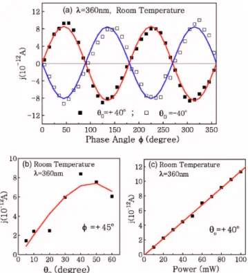
Figure2共a兲shows the helicity dependence of the photo-current at two different incident angles 共0= ± 40°, = 90°兲
with the radiation power of⬃70 mW. It clearly shows that the current reverses its direction by switching the sign of the radiation helicity and the incident angle. The CPGE current, which is proportional to the helicity, is only observed at ob-lique incidence. Figure2共b兲shows the incident angle0
de-pendence of the CPGE current with fixed radiation helicity and power of 70 mW. When the incident angle0was set to
zero, no current is created because there is no optically in-duced electron spin polarization in the plane of the sample according to the optical selection rules in semiconductor. Furthermore, we measured the photocurrent as a function of the radiation power. Figure 2共c兲 presents a linear relation between photocurrent and the radiation power up to the maximum of⬃100 mW. In all the above measurements, the azimuthal angleis kept at 90°.
The above experimental results can be fitted very well by Eq.共2兲, as shown by solid lines in Figs. 2共a兲–2共c兲, with
only one fitting parameter. Our observation is also consistent with that using intraband transition.10It is worth noting that the photocurrent in this measurement is almost one order of magnitude larger than that of the far-infrared radiation in GaN/AlGaN 2DEG.10 We believe that the larger photocur-rent indicates in our sample the larger spin splitting although the spin relaxation time is shorter共⬃14 ps兲. The main reason is that the spin-dependent photocurrent, induced by CPGE, is independent on the spin relaxation time.16
Figure 3 shows the angular dependence of the CPGE
FIG. 2.共Color online兲 The current is measured through AA⬘contact pair for direction perpendicular to propagation of incident light共= 90°兲. 共a兲 The phase angle dependence of CPGE photocurrent in the plane of GaN 2DEG sample共incident angle0= ± 40°兲. 共b兲 The incident angle0 depen-dence of the CPGE photocurrent with fixed radiation helicity. For both共a兲 and共b兲, the radiation power is 70 mW. 共c兲 The dependence of the radiation power共incident angle0= 40°兲. Measurements are carried out at room
tem-perature and irradiation by light at the wavelength of 360 nm.
FIG. 3.共Color online兲 Angular dependent investigations of CPGE photocur-rents. The inset diagram shows the geometry of the experiment. The currents are measured with oblique incident angle0= 40° and the radiation power of
70 mW共=360 nm兲.
252105-2 Zhao et al. Appl. Phys. Lett. 91, 252105共2007兲
current with the fixed radiation power at 70 mW and the incident angle at 40°. As indicated by Eq. 共2兲, the CPGE current j recorded from the AA⬘ contacts is proportional to sin while the sample is rotated around the normal. The advantage of this method is that only one contact pair was used to monitor the CPGE current. The difference induced by different contact pairs in the measurement of multicontact pair can be avoided. It is obvious that the CPGE current reaches the extrema共zero兲 when the propagation direction of the radiation light is perpendicular 共parallel兲 to the A-A⬘ direction. Again, this result can be fitted well with Eq. 共2兲. We note that the sign of the CPGE current reverses when the angle varies from negative to positive values. This obser-vation further supports the measured photocurrent results from the spin splitting in our GaN/AlGaN 2DEG sample. Furthermore, the CPGE photocurrent was measured similarly with all other contact pairs BB⬘, CC⬘, and DD⬘. When the propagation direction of incident light was perpendicular to the direction of any pair of the contacts, the CPGE photocur-rent in the plane of GaN 2DEG has essentially the same amplitude. These results indicated that there exists an isotro-pic in-plane spin splitting in GaN/AlGaN 2DEG.
In summary, we have observed the pure CPGE current at interband excitation by polarization-modulated radiation and a short spin relaxation time in wurtzite GaN/AlGaN 2DEG at room temperature. Using the angle dependent measure-ments of the magnitude of the photocurrent in the plane, we extracted direct information of the isotropic spin splittings in
k space in this system. These results, which are well
de-scribed by phenomenological theory, should help to shed light on our understanding of the SO coupling in GaN low-dimensional structure.
This work was supported by the Knowledge Innovation Project of the Chinese Academy of Sciences, the NSFC un-der the Grant No. 10504030, and the Chinese-French PRA
Project No. PRA MX06-07.
1S. A. Wolf, D. D. Awschalom, R. A. Buhrman, J. M. Daughton, S. Von
Molnàr, M. L. Rouke, A. Y. Chtchelka-nova, and D. M. Treger, Science 294, 1488共2001兲.
2Semiconductor Spintronics and Quantum Computation, edited by D. D.
Awschalom, D. Loss, and N. Samarth共Springer, Berlin, 2002兲, pp. 40–47.
3S. Datta and B. Das, Appl. Phys. Lett. 56, 665共1990兲.
4S. Murakami, N. Nagaosa, and S. C. Zhang, Science 301, 1348共2003兲. 5J. Sinova, D. Culcer, Q. Niu, N. A. Sinitsyn, T. Jungwirth, and A. H.
MacDonald, Phys. Rev. Lett. 92, 126603共2004兲.
6Y. K. Kato, R. C. Myers, A. C. Gossard, and D. D. Awschalom, Science
306, 1910共2004兲.
7J. Wunderlich, B. Kaestner, J. Sinova, and T. Jungwirth, Phys. Rev. Lett.
94, 047204共2005兲.
8R. Winkler, Spin-Orbit Coupling Effects in Two-Dimensional Electron and
Hole Systems, Springer Tracts in Modern Physics Vol. 191共Springer,
Ber-lin, 2003兲.
9V. I. Litvinov, Appl. Phys. Lett. 89, 222108共2006兲 and references therein. 10W. Weber, S. D. Ganichev, S. N. Danilov, D. Weiss, W. Prettl, Z. D. Kvon,
V. V. Bel’kov, L. E. Golub, H.-I. Cho, and J.-H. Lee, Appl. Phys. Lett. 87, 262106共2005兲.
11H. J. Chang, T. W. Chen, J. W. Chen, W. C. Hong, W. C. Tsai, Y. F. Chen,
and G. Y. Guo, Phys. Rev. Lett. 98, 136403共2007兲.
12B. K. Ridley, Appl. Phys. Lett. 77, 990共2000兲. 13V. I. Litvinov, Phys. Rev. B 68, 155314共2003兲.
14S. Schmult, M. J. Manfra, A. Punnoose, A. M. Sergent, K. W. Baldwin,
and R. J. Molnar, Phys. Rev. B 74, 033302共2006兲.
15Y. A. Bychkov and E. I. Rashba, Pis’ma Zh. Eksp. Teor. Fiz. 39, 66
共1984兲; JETP Lett. 39, 78 共1984兲.
16S. D. Ganichev and W. Prettl, J. Phys.: Condens. Matter 15, R935共2003兲. 17K. S. Cho, Y. F. Chen, Y. Q. Tang, and B. Shen, Appl. Phys. Lett. 90,
041909共2007兲.
18B. L. Liu, H. M. Zhao, J. Wang, L. S. Liu, W. X. Wang, D. M. Chen, and
H. J. Zhu, Appl. Phys. Lett. 90, 112111共2007兲.
19C. L. Yang, H. T. He, L. Ding, L. J. Cui, Y. P. Zeng, J. N. Wang, and W.
K. Ge, Phys. Rev. Lett. 96, 186605共2006兲.
20B. Beschoten, E. Johnston-Halperin, D. K. Young, M. Poggio, J. E.
Grim-aldi, S. Keller, S. P. DenBaars, U. K. Mishra, E. L. Hu, and D. D. Aw-schalom, Phys. Rev. B 63, 121202共2001兲.
21M. I. D’yakonov and V. I. Perel, Sov. Phys. Solid State 13, 3023共1972兲.
252105-3 Zhao et al. Appl. Phys. Lett. 91, 252105共2007兲
Experimental Study on the Spin-Orbit Coupling Property in Low-dimensional Semiconductor Structures
Published Papers related to the Thesis
XVII
3. Electron spin quantum beats and room temperature g factor in
GaAsN
Appl. Phys. Lett. 95, 041911 (2009)
Experimental Study on the Spin-Orbit Coupling Property in Low-dimensional Semiconductor Structures
Electron spin quantum beats and room temperature g factor in GaAsN
H. M. Zhao,1L. Lombez,2B. L. Liu,1,a兲B. Q. Sun,3Q. K. Xue,1D. M. Chen,1and X. Marie2,b兲
1
Beijing National Laboratory for Condensed Matter Physics, Institute of Physics, Chinese Academy of Sciences, P.O. Box 603, Beijing 100080, People’s Republic of China
2
Université de Toulouse, INSA-CNRS-UPS; LPCNO, 135 av. de Rangueil, 31077 Toulouse, France
3
State Key for Superlattices and Microstructures, Institute of Semiconductors, Chinese Academy of Sciences, P.O. Box 912, Beijing 100083, People’s Republic of China
共Received 2 March 2009; accepted 3 July 2009; published online 31 July 2009兲
We report on the investigation of electron spin quantum beats at room temperature in GaAsN thin films by time-resolved Kerr rotation technique. The measurement of the quantum beats, which originate from the Larmor precession of electron spins in external transverse magnetic field, yields an accurate determination of the conduction electron g factor. We show that the g factor of GaAs1−xNx thin films is significantly changed by the introduction of a small nitrogen fraction.
© 2009 American Institute of Physics.关DOI:10.1063/1.3186076兴
The substitution of small amounts of nitrogen at anion sites in certain III-V semiconductors 共GaAs, InGaAs, GaP兲 drastically modifies the optical and electronic properties of these materials that are important for optoelectronic device applications.1–6 Very recent results have shown that these dilute nitrides compounds possess, furthermore, the remark-able property of a very large and robust electron spin polar-ization even at room temperature 共RT兲, which could confer them an important role in the spintronics field.7–11The un-usual electron spin properties of dilute nitrides are due to a
spin dependent recombination 共SDR兲 process on deep
paramagnetic centers, observed initially in silicon12 and 共Al兲GaAs 共Refs. 13 and 14兲 and only very recently in
GaAsN 共Refs. 7, 8, and 15兲 with record high values. The
manipulation of electron spin with an external magnetic field requires the knowledge of the electron Landé g factor in this material. Magnetoabsorption experiments were performed recently in 共In兲GaAsN at low temperature 共T⬍30 K兲;16,17 however, the nitrogen dependence of the g factor at RT has not been studied yet.
In this letter, we have measured at RT the electron g factor in GaAsN thin films for different nitrogen composi-tions by time-resolved optical orientation experiments.18The value of 兩g兩 is determined from the direct measurement of Larmor precession periods under different transverse mag-netic fields. We used a pump-probe time-resolved Kerr rota-tion 共TRKR兲 technique to generate electron spins and mea-sure its time evolution in a transverse magnetic field 共B is applied perpendicular to the growth direction兲.19
This tech-nique is very powerful to determine the Larmor precession frequency as a function of the magnetic field applied in the sample.20 Compared to magneto-optical experiments per-formed in the spectral domain, this time-resolved technique allows us to measure with great accuracy the absolute value of the effective electron g factor. The advantage of the g factor measurement in the time domain is that it permits the accurate determination of the Zeeman splitting between states without resolving them spectrally.18,20 Thanks to the
subpicosecond time resolution, the time-resolved Kerr rota-tion measurements yield a precision of ⌬g/g= ⫾5.10−3,
whereas ⌬g/g⬃ ⫾10−1 or more in cw magneto-optical
experiments.16,17
Three samples were grown on a semi-insulating 共001兲-oriented GaAs substrate by molecular beam epitaxy. The thickness and the composition of the GaAs1−xNxfilms were
controlled with in situ intensity oscillations of reflection high energy electron diffraction and x-ray measurements. For samples A–C, the nitrogen fractions are 0.09%, 0.65%, and 0.9% with film widths of 390, 480, and 190 nm, respectively. The TRKR experiment was carried out in an Oxford optical cryostat supplied with a 7-T super conducting split coil magnet. The samples, at room temperature, are excited near normal incidence with degenerate pump and delayed probe pulses from a Coherent mode-locked Ti:sapphire laser 共⬃120 fs, 76 MHz兲. Its wavelength is tuned to get maxi-mum Kerr rotation signal for each sample. The laser beams are focused to a spot size of ⬃100 m, and the pump and probe beams have average power intensities of 10 and 2 mW, respectively. The helicity of linearly polarized pump beam is modulated at 50 kHz by a photoelastic modulator for lock-in detection. The normal component of net spin throughout the GaAsN layer is measured by the Kerr rotation angle K of
the linearly polarized probe pulse. Note that the pump exci-tation power is kept low enough in order to avoid SDR effect due to the dynamical polarization of the deep paramagnetic centers. The SDR effect, observed for large excitation pow-ers, yields strong and robust spin polarization but it could complicate the interpretation of the spin quantum beat ex-periments 共as the spin precession of both free electrons and localized electrons on the deep centers should be taken into account兲.8,10 At low excitation intensity, SDR is negligible and the measured spin dynamics correspond simply to the free electron spin polarization.
Figure 1 shows the transient Kerr rotation responses in sample C共nitrogen fraction: 0.9%兲 for different values of the transverse magnetic field. The signal shows strong oscilla-tions corresponding to the spin precession with an exponen-tial decay envelope. The monoexponenexponen-tial decay 共⬃60 ps兲 results from spin relaxation and carrier recombination. It is well known that the hole spin relaxation time is extremely
a兲Electronic mail: [email protected]. b兲Electronic mail: [email protected].
APPLIED PHYSICS LETTERS 95, 041911共2009兲
0003-6951/2009/95共4兲/041911/3/$25.00 95, 041911-1 © 2009 American Institute of Physics