Control of buckling in large micromembranes
using engineered support structures
The MIT Faculty has made this article openly available.
Please share
how this access benefits you. Your story matters.
Citation
Iwase, Eiji, Pui-Chuen Hui, David Woolf, Alejandro W Rodriguez,
Steven G Johnson, Federico Capasso, and Marko Lončar. “Control
of buckling in large micromembranes using engineered support
structures.” Journal of Micromechanics and Microengineering 22,
no. 6 (June 1, 2012): 065028.
As Published
http://dx.doi.org/10.1088/0960-1317/22/6/065028
Publisher
IOP Publishing
Version
Author's final manuscript
Citable link
http://hdl.handle.net/1721.1/81261
Terms of Use
Creative Commons Attribution-Noncommercial-Share Alike 3.0
Control of buckling in large nanomembranes using engineered support structures
Eiji Iwase1, Pui-Chuen Hui1, David Woolf1, Alejandro W. Rodriguez1,2, Steven G. Johnson2, Federico Capasso1, Marko Loncar1
1
School of Engineering and Applied Sciences, Harvard University, Cambridge, Massachusetts 02138, USA
2Department of Mathematics, Massachusetts Institute of Technology, Cambridge, Massachusetts 02139, USA
In this paper we describe a general method to avoid stress-induced buckling of thin and large freestanding membranes. We show that using properly designed supports, in the form of nanobeams, it is possible to reduce the out-of-plane deflection of the membrane while maintaining its stiffness. As a proof of principle, using silicon-on-insulator (SOI) platform, we realized 30-µm-wide, 220-nm-thick, free-standing Si membranes, supported by four 15-µm-long and 3-µm-wide nanobeams. Using our approach, we were able to achieve out-of-plane deformation of the membrane smaller than 50 nm in spite of 39 MPa of compressive internal stress. Our method is general, and can be applied to different material systems with compressive or tensile internal stress.
1. Introduction
Freestanding micro membrane structures are commonly used in microelectromechanical systems (MEMS) to realize, for example, variable capacitors [1], RF switches [1],[2], pressure sensors [3], movable mirrors [4]. In such freestanding structures, deformation by residual internal stress is a well known issue [5]-[7]. The stress, caused by the difference in thermal expansion coefficients of different materials, is often built-in during the process of thin film deposition and is therefore difficult to avoid. This is a problem since large compressive or tensile stress can lead to buckling or breaking of the membrane. The degree of buckling depends on the length/thickness ratio of a membrane structure: if the ratio is 100 or larger buckling can be significant even for low values of compressive stress (on the order of several tens of MPa). To reduce the effect of the internal stress, stress-reduction techniques based on the optimization of the deposition conditions [8], post-deposition annealing [9], stress-compensation by a post-deposition of another film [4], and ion implantation [9],[10] have been investigated. These are however material-specific solutions, and therefore cannot be applied in all situations. Moreover these stress compensation methods do not work at high temperatures because of the different thermal expansion coefficients. In this paper, we describe general method to control the out-of-plane strain and stiffness by using properly designed supporting beam structure. We use this method to realize large, free-standing Si membranes perforated with lattice of holes to define photonic
crystal (PhC) structure as shown in Figure 1.
Recently, there has been a lot of interest in realization of PhC membranes that support guided resonances for applications in the field of optomechanics [11]-[17]. These membranes are typically realized in semiconductor materials with large optical index, e.g. Si or InGaAs. To ensure a strong optomechanical interaction, thin (~ 200 nm) and large (~ several tens of µm) membrane structures, with length/thickness ratio of ~100, are desired. The small thickness allows for greater flexibility of the membrane (to enable strong response of the structure to the weak forces), while the large area is needed to assure good confinement of guided resonances supported by the membrane. Furthermore, the membrane and the substrate are separated by as few as hundreds of nm [12],[14]-[16], in order to enhance the optomechanical coupling. For all of these reasons, it is essential to reduce buckling of the membrane due to built-in internal stress and avoid failure of the structure.
2. Design
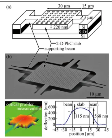
A 2-D PhC slab structure that supports guided resonances, and that we are interested in studying in this work, is shown in Figure 1(a). It consists of a 220-nm-thick free-standing (square-shaped) Si membrane of width 30 µm, supported by four nanobeams of length 15 µm. The membrane is perforated with PhC lattice of holes with periodicity a = 1 µm and hole radius of r = 200 nm. The structure was realized in a commercial SOI wafer (SOITEC Inc.) with 220-nm-thick Si device layer and 2-µm-thick BOX (buried oxide) layer. The structure was fabricated using electron beam lithography followed by inductive coupled plasma reactive ion etching (ICP RIE) and HF vapor etching. As shown in Figure 1(b), the 2-D PhC slab structure with simple straight supporting beams is buckled by its own internal stress. Our approach is to design beam structures in order to avoid the out-of-plane deformation without changing the out-of-plane stiffness of beams.
In the case of a simple beam structure with l, w, t in length, width and thickness respectively, a critical buckling stress σc is proportional to the inverse second power of the length/thickness ratio. In the case of doubly-clamped beams, the critical buckling stress is given by σc=π2
3𝐸 � 𝑡 𝑙�
2
, where E is the Young’s modulus of the structure. If the structure has a
compressive internal stress σ0 larger than the critical buckling stress (σ0≥ σc), then critical buckling length 𝑙c=π𝑡� 𝐸
3σ0 can be defined so that all the beams with length l > lc will be buckled. Critical buckling length for t = 200 nm thick device layer of
SOI wafer can be estimated to be in the range of lc = 13-41 µm, taking into account the internal stress of σ0 = 10–100 MPa
typical in commercial SOI wafers and Young’s modulus of Si for the <110> direction of 169 GPa. Therefore, buckling can be large even in a structure with several tens of µm in length (Figure 2(a)). We note that the critical buckling length increases to
lc = 196-620 µm if the thickness of the Si device layer is increased to t = 3 µm. To evaluate the built-in stress in the wafers
used in this experiment, we fabricated arrays of doubly-clamped beams with varying length and measured their out-of plane deflection using a 3-D optical profiler (Olympus LEXT OLS4000, display resolution: 1 nm). The results, shown in Figure
2(b), are in good agreement with the theoretical model discussed above. Using these values, we estimated the compressive internal stress of the Si device layer of the SOI to be 39 MPa, resulting in critical buckling length lc = 26.3 µm. This explains
significant buckling of PhC membrane (Figure 1) with total length larger than lc.
In order to overcome buckling issue, it is necessary to engineer the supporting beams. Fundamentally, buckling appears when a compressive internal stress acts as an axial load to a supporting beam (Figure 3(a)). Therefore, our design methods are classified into three categories based on the type of the deflection induced by compressive stress. “Type 1” method leads to in-plane buckling instead of out-of-plane buckling (Figure 3(b)) due to axial load. “Type 2” method leads to in-plane deformation without buckling (Figure 3(c)) due to axial load. This is achieved by taking advantage of beams with an initial deflection (i.e. curved beams). Type 2 beams can be deformed below the in-plane critical buckling stress, whereas Type 1 beams are deformed only by the in-plane critical buckling stress or more. “Type 3” method uses a lateral beam in order to act compressive stress as a lateral load. (Figure 3(d)). Type 2 and Type 3 can be described as methods of releasing the internal stress by in-plane deformation.
For the Type 1 method to work it is important that in-plane critical buckling stress 𝜋2
3 𝐸 � 𝑤
𝑙� 2
is smaller than the
out-of-plane critical buckling stress π2
3 𝐸 � 𝑡 𝑙�
2
. Therefore, an extremely narrow and long beam is required which may be challenging to implement. In addition, Type 1 is only effective in the case of compressive stress, while Type 2 and Type 3 can be used for both compressive and tensile stress.
Types 2 and 3 are based on the similar idea: the stiffness of a simple straight beam against an axial load (i.e. in-plane stiffness) is 𝐸𝑤𝑡
𝑙. Therefore, if part of the beam has in-plane stiffness smaller than 𝐸 𝑤𝑡
𝑙, the part can relieve the internal stress
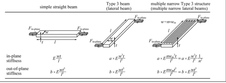
by its elastic deformation. However, we do not want to reduce the out-of-plane stiffness (i.e. out-of-plane spring constant), because the supporting beams have to play two roles: (1) reducing the out-of-plane deformation and (2) supporting the membrane structure. Therefore we use a “multiple narrow beam structure”, shown in Table 1. Table 1 shows the in-plane and out-of-plane stiffness of a simple straight beam and Type 3 beams. Using a “multiple narrow beam structure” it is possible to reduce the in-plane stiffness while maintaining the same out-of-plane stiffness, compared to a simple straight beam. That is, if we change from a simple lateral beam to n beams with 1 𝑛⁄ in width, we can get 1 𝑛⁄ times smaller stiffness in the in-plane 2 direction while maintaining the same out-of-plane stiffness (shown in Table 1). The same analysis applies to Type2 beams, and is shown in Table 2.
3. Fabrication and evaluation
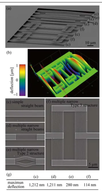
To verify our designs, we fabricated the structures discussed in previous section, using the same SOI wafer as in Figure 2. The SEM images and the beam deflections measured using a 3-D optical profiler are shown in Figure 4. The length,
width and thickness of the beams are 100 µm, 3 µm and 220 nm, respectively. Figure 4(c) shows a simple straight beam with 1,212 nm of out-of-plane deflection due to buckling. Figure 4(e) shows multiple narrow Type 2 structures which consist of 8 narrow curved beams with 200 nm widths. Figure 4(f) shows multiple narrow Type 3 structures which consist of 15 narrow lateral beams with 200 nm widths. Maximum deflections of the multiple-narrow Type 2 and Type 3 structures are 280 nm and 114 nm, respectively. As can be seen, the out-of-plane deflections are highly reduced using our proposed methods. Figure 4(d) is a beam with multiple narrow straight beams without initial deflection, so the beam also suffers out-of-plane buckling of 1,211 nm. Though we could not measure the in-plane deformation in Figure 4(e), we can obviously confirm the effect of initial deflection (i.e. curved beam) by comparing to the out-of-plane deflection of Figure 4(d).
Figure 1(b) and Figure 5(a), (b) show the photonic crystal membrane structures with simple, Type 2 and Type 3 supporting beams, respectively. Using the profiler, we measured the maximum deflections of Type 2 and Type 3 to be 49 nm and 33 nm, respectively. This is more than an order of magnitude smaller than a maximum deflection (568 nm) measured for the membrane with simple supporting beams (Figure 1(b)). Finally, we note that since the supporting beams relieve the internal stress, the membrane itself does not bend (below the resolution of our apparatus) under to the internal stress, and is very flat. This is of great importance for photonic applications that we envisioned.
4. Discussion
Approaches to reduce the out-of-plane buckling/deflection by designing proper supports, using methods that fall in categories Type 2 [18] or Type 3 [19],[20], have previously been studied. The novel aspect of our work is application of multiple narrow beam structures that offer very important advantages over other methods: in-plane and out-of-plane stiffness can be designed almost independently. That is, by increasing n, we can reduce the in-plane stiffness of the beam without changing the out-of-plane stiffness.
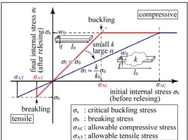
In the case of simple beam, the internal stress before (σ0) and after (σf) releasing are the same, up to the critical buckling stress σc or the breaking stress σb (Figure 6). Therefore the simple beam can be used as long as the internal stress σ0 is a value between σc and σb. In the case of Type 2 or Type 3 beams, with smaller in-plane stiffness, σ0 and σf are different
due to the in-plane elastic deformation of the beam. Therefore, we define two new parameters allowable compressive stress
σAC and allowable tensile stress σAT defined in a following way: if the initial stress σ0 is σAC and σAT, the final stress σf would be σc and σb, respectively (see Figure 6). As a result, Type 2 and Type 3 beams can be used as long as the initial internal stress σ0 has a value between σAC and σAT. In the case of the multiple narrow beam structure, σAC and σAT are proportional to n
2
. Therefore it is always possible choose n which satisfies this condition, which makes approach general and useful for range of geometries and films deposited using different techniques. However, in practice the upper limit of n is set by the minimum resolution of the fabrication process, since the larger the n, the smaller the width of each beam in multi-beam section. If the
characteristic beam width is w0 and the minimum available width on the fabrication is wmin, n should be smaller than
𝑤0⁄𝑤min. For example our characteristic beam width was 3 µm and the minimum resolution is approximately 50 nm because
of electron beam lithography, so the upper limit of n is 60. As we mentioned, the allowable stresses σAC and σAT are
proportional to n2, so our method can deal with wide range of the internal stress. This is another unique feature of our method, and has not been investigated before. The approach is material-platform agnostic which further adds to its versatility. In addition, because our method can release internal stress of any magnitude as long as the stress is smaller than the allowable internal stresses, we do not have to know the precise internal stress of the membrane. In other words, if we choose a large enough value n, our beams make proper in-plane deformations according to the magnitude of internal stress, automatically. This is very effective, especially for mitigation of temperature induced stress the value of which can greatly vary with temperature: our approach’s “self-adaptability” to internal stress makes it effective for a wide range of temperatures.
Though our method highly reduced the out-of-plan deflection, the structures still have finite deflection < 50 nm. We believe that this is due to stress gradient of the membrane and/or a bending moment at its ends, which also can cause asymmetric upward and downward deflections. Indeed, it can be seen in Figure 2(b) that the upward and downward deflections are slightly different (~ 80 nm). The stress gradient comes from the wafer fabrication process and the bending moment at the ends comes from the residue of the sacrificial layer under the membrane. Since the 2-D PhC slab region is very flat (in Figure 5(a), (b)) and the most of the deflection is due to the supporting beam region, we can conclude that the residual deflection is not due to the stress gradient, but rather due to the bending moment at the beam ends. Though our method cannot deal with a stress gradient and a bending moment at the ends, these effects cause little deflection.
5. Conclusions
We proposed a method to reduce the out-of-plane deflection of a membrane structure due to its internal stress, while maintaining the out-of-plane stiffness of the structure. Using the multiple narrow Type 2 and Type 3 supporting beam structures, it is possible to precisely engineer the residual stress simply by changing number of beams (n). Applying our methods to a commercial SOI wafer with 39 MPa of compressive internal stress, we were able to reduce the out-of-plane deflection of the freestanding membrane for more than order of magnitude, from 568 nm to below 50 nm. In the cases of Type 2 and Type 3 structures, the maximum deflections were 49 nm and 33 nm, respectively. The characteristic length and thickness of the membrane structure is 60 µm and 220 nm, respectively, so that the length/thickness ratio of our membrane structure is 273 and the maximum deflection/length ratio is less than 1/1,000. These values mean the freestanding thin and large membrane structure has little out-of-plane bending. In addition, our method can deal with a range of stress values and therefore it is suitable for compensation of not only the compressive but also the tensile internal stress. Furthermore, it can be used at high temperature, since it can handle temperature induced stress.
Acknowledgement
This work was supported by the Defense Advanced Research Projects Agency (DARPA) under Contract No. N66001-09-1-2070-DOD. The deflection measurement was performed by the 3-D optical profiler Olympus LEXT OLS4000 owned by Prof. Robert Woods at Harvard University. The microstructure fabrication was carried out using the facilities of Center for Nanoscale Systems (CNS) at Harvard University.
Figure legends
Figure 1 (a) Schematic image of a target structure and the typical lengths. The structure consists of the thin and large 2-D PhC slab and supporting beams. (b) Buckling of the thin and large membrane structure by its own internal stress.
Figure 2 Deformation by the internal stress on a commercial SOI wafer with 220 nm in a device layer thickness t. (a) The doubly-clamped beams are buckled upward or downward. (b) Evaluation of the internal stress. Each length of the beams is l = 4, 10, 20, 30, 40, 50, 60, 70, 80, 90, 100 µm. The horizontal axis is an effective beam length leff which means that designed
beam length l plus a constant undercut-length. In this graph, undercut length is 23 µm. Blue and red dots are deflections of upward and downward buckling, respectively. Error bars refer to the standard deviations. The difference between upward and downward buckling should be come from stress gradient and bending moment at the ends. The dashed line is a fitting curve
of a theoretical deflection 𝑣max= 2
�
σ0𝐸 𝑙eff2
π2 −
𝑡2
3 [5] under σ0.of 39 MPa.
Figure 3 Classification of beam structure that overcome out-of-plane buckling due to an axial load. The principle is based on inducing in-plane deformation to overcome out-of-plane one due to an axial load.
Table 1 In-plane and out-of-plane stiffness of a simple straight beam and Type 3 beams. Stiffness is defined by a load/deformation ratio (i.e. 𝐹 𝑣⁄ 𝑚𝑎𝑥). In the case of a simple straight beam, the in-plane stiffness is 𝐸𝑤𝑡
𝑙 and the out-of-plane
stiffness is proportional to 𝐸𝑤𝑡3
𝑙3 . The coefficients a, b are determined by load and end conditions. For example, in the case of
a doubly-clamped beam under point loading at the center, a=b=16. In the case of a guided-clamped beam under point loading at the free end, a=b=1.
Table 2 In-plane and out-of-plane stiffness of Type 2 beams. We can use the same analysis as with the Type 3 under the assumption that length/width ratio is large.
Figure 4 Doubly-clamped beams with various beam structures. All beams are 100 µm long and 3 µm wide. (a) SEM image of the beams. (b) Measurement of the deflections by a 3-D optical profiler. (c), (d), (e), (f) Enlarged images of each beam structure before releasing. (g) Table showing the maximum deflection of the beams.
Figure 5 2-D PhC slab structures with supporting beams. The period and hole radius of the PhC slab is 1 µm and 200 nm, respectively. The length and width of the slab is 30 µm by 30 µm, and characteristic length and width of the supporting beams are 15 µm and 3 µm, respectively. (a) and (b) are structures with multiple-narrow Type 2 and Type 3 structures, respectively. Structure with simple beams, fabricated on the same wafer, is shown in Figure 1(b). The “noise” in the measurement at the position of the slab is due to the photonic crystal holes with sizes below the resolution limit of the profilometer.
Figure 6 Controlling the allowable stress using engineered support structures: The released membrane structure is flat when (no buckling) when the final internal stress after releasing σf is between σc and σb, where σc and σb are the critical buckling stress and the breaking stress, respectively. This corresponds to an initial internal stress before releasing σ0, it means that σ0 is a value betweenσAC and σAT, where σAC and σAT are the allowable compressive and tensile stress, respectively. In the case of
a simple straight beam, σAC and σ AT should be the same as σc and σb, respectively. But the beam has smaller stiffness beam
with k in the in-plane stiffness, σAC and σAT is enlarged approximately as 𝑘0
𝑘σc and 𝑘0
𝑘σb, where 𝑘0= 𝐸 𝑤0𝑡
𝑙0 , l0 is the beam
length from end to end, and w0 is the beam width at the end. If the multiple-narrow Type 2 or Type 3 structure is used, the
in-plane stiffness k is described by the formula 𝑘 = 𝑎
𝑛2𝐸𝑤 3𝑡
𝑙3 as shown in Table 1 and 2.
References
[1] J. J. Yao, “RF MEMS from a Device Perspective,” Journal of Micromechanics and Microengineering, vol. 10, pp. R9-R38, 2000.
[2] G. M. Rebeiz, J. B. Muldavin, “RF MEMS Switches and Switch Circuits,” IEEE Microwave Magazine, vol. 2, pp. 59-71, 2001.
[3] W. P. Eaton, J. H. Smith, “Micromachined Pressure Sensors: Review and Recent Developments,” Smart Materials and
Structures, vol. 6, pp. 530-539, 1997.
[4] Y. H. Min, Y. K. Kim, “Modeling, Design, Fabrication and Measurement of a Single Layer Polysilicon Micromirror with Initial Curvature Compensation,” Sensors and Actuators A-Physical, vol. 78, pp. 8-17, 1999.
[5] W. Fang, J. A. Wickert, “Post Buckling of Micromachined Beams,” Journal of Micromechanics and Microengineering, vol. 4, pp. 116-122, 1994.
[6] W. Fang, J. A. Wickert, “Determining Mean and Gradient Residual Stresses in Thin Films Using Micromachined Cantilevers,” Journal of Micromechanics and Microengineering, vol. 6, pp. 301-309, 1996.
[7] S. Creek, N. Chitica, “Deflection of Surface-Micromachined Devices Due to Internal, Homogeneous or Gradient Stresses,” Sensors and Actuators A-Physical, vol. 78, pp. 1-7, 1999.
[8] X. A. Fu, R. Jezeski, C. A. Zorman, M. Mehregany, “Use of Deposition Pressure to Control Residual Stress in Polycrystalline SiC Films,” Applied Physics Letters, vol. 84, p. 341, 2004.
[9] J. Camassel, A. Tiberj, “Strain Effects in Device Processing of Silicon-on-Insulator Materials,” Applied Surface Science, vol. 212, pp. 742-748, 2003.
[10] T. G. Bifano, H. T. Johnson, P. Bierden, R. K. Mali, “Elimination of Stress-Induced Curvature in Thin-Film Structures,”
Journal of Microelectromechanical Systems, vol. 11, pp. 592-597, 2002.
[11] W. Suh, M. F. Yanik, O. Solgaard, S. H. Fan, “Displacement-Sensitive Photonic Crystal Structures Based on Guided Resonance in Photonic Crystal Slabs,” Applied Physics Letters, vol. 82, pp. 1999-2001, 2003.
[12] M. Notomi, H. Taniyama, S. Mitsugi, E. Kuramochi, “Optomechanical Wavelength and Energy Conversion in High-Q Double-Layer Cavities of Photonic Crystal Slabs,” Physical Review Letters, vol. 97, 023903, 2006.
[13] Y. Kanamori, T. Kitani, K. Hane, “Control of Guided Resonance in a Photonic Crystal Slab Using Microelectromechanical Actuators,” Applied Physics Letters, vol. 90, 031911, 2007.
[14] Y. G. Roh, T. Tanabe, A. Shinya, H. Taniyama, E. Kuramochi, S. Matsuo, T. Sato, M. Notomi, “Strong Optomechanical Interaction in a Bilayer Photonic Crystal,” Physical Review B, vol. 81, 121101, 2010.
[15] A. W. Rodriguez, D. Woolf, P. C. Hui, E. Iwase, A. P. McCauley, F. Capasso, M. Loncar, S. G. Johnson, “Designing Evanescent Optical Interactions to Control the Expression of Casimir Forces in Optomechanical Structures,” Applied
Physics Letters, vol. 98, 194105, 2011.
[16] A. W. Rodriguez, A. P. McCauley, P. C. Hui, D. Woolf, E. Iwase, F. Capasso, M. Loncar, S. G. Johnson, “Bonding, Antibonding and Tunable Optical Forces in Asymmetric Membranes,” Optics Express, vol. 19, pp. 2225-2241, 2011.
[17] L. Midolo, P. J. van Veldhoven, M. A. Dundar, R. Notzel, A. Fiore, "Electromechanical Wavelength Tuning of Double-Membrane Photonic Crystal Cavities," Applied Physics Letters, vol. 98, 211120, 2011.
[18] A. M. Elshurafa, E. I. El-Masry, “Finite-Element Modeling of Low-Stress Suspension Structures and Applications in RF MEMS Parallel-Plate Variable Capacitors,” IEEE Transactions on Microwave Theory and Techniques, vol. 54, pp. 2211-2219, 2006.
[19] A. P. Pisano, Y. H. Cho, “Mechanical Design Issues in Laterally-Driven Microstructures,” Sensors and Actuators
A-Physical, vol. 23, pp. 1060-1064, 1990.
[20] D. J. Young, B. E. Boser, V. Malba, A. F. Bernhardt, “A Micromachined RF Low Phase Noise Voltage-Controlled Oscillator for Wireless Communications,” International Journal of RF and Microwave Computer-Aided Engineering, vol. 11, pp. 285-300, 2001.
Figure 1 (a) Schematic image of a target structure and the typical lengths. The structure consists of the thin and large 2-D PhC slab and supporting beams. (b) Buckling of the thin and large membrane structure by its own internal stress.
Figure 2 Deformation by the internal stress on a commercial SOI wafer with 220 nm in a device layer thickness t. (a) The doubly-clamped beams are buckled upward or downward. (b) Evaluation of the internal stress. Each length of the beams is l = 4, 10, 20, 30, 40, 50, 60, 70, 80, 90, 100 µm. The horizontal axis is an effective beam length leff which means that designed beam length l
plus a constant undercut-length. In this graph, undercut length is 23 µm. Blue and red dots are deflections of upward and downward buckling, respectively. Error bars refer to the standard deviations. The difference between upward and downward buckling should be come from stress gradient and bending moment at the ends. The dashed line is a fitting curve of a theoretical deflection 𝑣max= 2�σ𝐸0𝑙eff
2
π2 −𝑡 2
3 [5] under σ0.of 30 MPa.
Figure 3 Classification of beam structure that overcome out-of-plane buckling due to an axial load. The principle is based on inducing in-plane deformation to overcome out-of-plane one due to an axial load.
Table 1 In-plane and out-of-plane stiffness of a simple straight beam and Type 3 beams. Stiffness is defined by a load/deformation ratio (i.e. 𝐹 𝑣⁄ 𝑚𝑎𝑥). In the case of a simple straight beam, the in-plane stiffness is 𝐸𝑤𝑡
𝑙 and the
out-of-plane stiffness is proportional to 𝐸𝑤𝑡3
𝑙3 . The coefficients a, b are determined by load and end conditions. For example, in
the case of a doubly-clamped beam under point loading at the center, a=b=16. In the case of a guided-clamped beam under point loading at the free end, a=b=1.
Table 2 In-plane and out-of-plane stiffness of Type 2 beams. We can use the same analysis as with the Type 3 under the assumption that length/width ratio is large.
Figure 4 Doubly-clamped beams with various beam structures. All beams have 100 µm in length and 3 µm in width. (a) SEM image of the beams. (b) Measurement of the deflections by a 3-D optical profiler. (c), (d), (e), (f) Enlarged images of each beam structure before releasing. (g) Table of the maximum deflection of the beams.
Figure 5 2-D PhC slab structures with supporting beams. The period and hole radius of the PhC slab is 1 µm and 200 nm, respectively. The length and width of the slab is 30 µm by 30 µm, and characteristic length and width of the supporting beams are 15 µm and 3 µm, respectively. (a) and (b) are structures with multiple-narrow Type 2 and Type 3 structures, respectively. Structure with simple beams, fabricated on the same wafer, is shown in Figure 1(b). The “noise” in the measurement at the position of the slab is due to the photonic crystal holes with sizes below the resolution limit of the profilometer.
Figure 6 Controlling the allowable stress using engineered support structures: The released membrane structure is flat when (no buckling) when the final internal stress after releasing σf is between σc and σb, where σc and σb are the critical buckling stress and the breaking stress, respectively. This corresponds to an initial internal stress before releasing σ0, it means that σ0 is a value between σAC and σAT, where σAC and σAT are the allowable compressive and tensile stress, respectively. In the case of a simple straight beam, σAC and σ AT should be the same as σc and σb, respectively. But the beam has smaller stiffness beam with k in the in-plane stiffness, σAC and σAT is enlarged approximately as 𝑘𝑘0σc and 𝑘𝑘0σb,
where 𝑘0= 𝐸𝑤0𝑡
𝑙0 , l0 is the beam length from end to end,
and w0 is the beam width at the end. If the
multiple-narrow Type 2 or Type 3 structure is used, the in-plane stiffness k is described by the formula 𝑘 = 𝑎
𝑛2𝐸𝑤 3𝑡
𝑙3 as