Zeitschrift fürPhysikalischeChemie, Bd. 208,S. 107-136(1999) © byR. Oldenbourg Verlag, München 1999
Copper Electrodeposition
on
Alkanethiolate
Covered
Gold Electrodes*
By
O.Cavalleri,
A. M.Bittner**,
H.Kind,
K. KernInstitut de
Physique
Expérimentale,EcolePolytechniqueFédéraledeLausanne, CH-1015 Lausanne,SwitzerlandandT. Greber
Physik-Institut, UniversitätZürich,CH-8057Zürich,Switzerland
(ReceivedDecember 1, 1997;
accepted
December23, 1997)Cyclic voltammetry
IFilmgrowth
IScanning tunnelling
microscopy
(STM)
ISingle crystal
electrode ISurface
structureIThiolsIX-ray photoelectron
spectroscopy
(XPS)
We have investigated the structure and thermal dynamics of alkanethiolate layers on
Au(Hl)with variabletemperaturescanning tunnelling microscopy(STM), X-ray
photo-electronspectroscopy (XPS)and voltammetry.Theresults build the basis fora studyof
electrodeposition of copper on alkanethiolate-covered Au(lll).
Electrodeposition
has been studied as a function ofthe thiolate chainlength, thedepositionpotential
and thetemperature. Time-resolved in situ STM and voltammetry, both at temperatures up to
345K,andXPS of emersedsamplesshowed thatcoppercan
—
depending
onthe
deposi-tion potential
—
eitherformnanometer-sizedislands orlayers, both withoutdestruction ofthe thiolate. We proposeamechanism wherecopperpenetratesthe thiolatelayer. The
slowdeposition rate isdetermined
only by
kineticfactors since Cu/Cu2+ exchangepro-cessescannotoperate.
Finally
wediscuss therole of thiolatesaspreadsorbedsurfactants.1. Thiolate
layers
and the
electrodeposition
of metals
Certain chemical elements or
molecules,
especially
soft bases such asiodide, bromide,
sulphide,
carbon monoxide andcyanide,
areknown tobind withexceptional
strength
tonoble metal surfaces. In electrochemical terms,the substances adsorb
specifically.
Suchadlayers
are oftendensely packed,
hence the atoms or molecules
prefer (quasi)-hexagonal
arrangements
[1—7].
* Presented at the 5. Ulmer Elektrochemische Tage on "Fundamental Aspects of
Electrolytic
MetalDeposition",
June23-24, 1997.**
The
adlayer
geometry is determinedby
theinterplay
ofadsorbate-sub-strate forces that tend to direct the
adsorbing
atoms toplaces
that offer astrong
bond(often
hollowsites)
and interadsorbate forces thatcanbeattrac-tive or
repulsive.
Morecomplex,
but also muchmoreversatile,
are thiolateadsorbates. Alkanethiols
CH3(CH2)„ iSH
('C„
thiols')
formstrongly
adsorb-ed,
ordered thiolatelayers
CH3(CH2)„_,S/substrate [8-10].
Although
theadsorption
process does not differprincipally
from the above-mentionedcases,theterm
'self-assembly'
isemployed
topoint
outthat thiolate interad-sorbate forces are verystrong
—
long adsorption
times are necessary to assemble an ordered structure where the
alkyl
chainsalign
parallel.
Up
tonow,
mainly
theAu(lll)
substrate wasused;
its reconstruction isreadily
lifted
during
theadsorption.
Several studies of vacuum metal
deposition
on thiolate-covered metalsubstrates wereconducted;
Jung
and Czandernacompiled
avaluable review[11].
Theelectrodeposition
ofmetals,
e.g. copper, onthiolatelayers
istech-nically
muchsimpler,
but moredifficulttointerpret
: onehastoconsider the electrodepotential. Especially
the Cu2+/Cuequilibrium
(Nernst)
potential
isimportant.
Positive of thatpoint,
copper canonly deposit
in asingle layer
and
only
on somespecial
substrates(underpotential deposition,
UPD) [12—
17].
Negative
ofit,
normal copper bulkdeposition
takesplace
on anysub-strate
(overpotential
deposition,
OPD).
Electrodeposition
of Cu2+ in the OPD range often results in 3Dgrowth
of copperonmetal substrates ase.g.found with in situ STM
[12a, 18-23].
A similar situation shows up when copper is
deposited
onalkanethiol-ate-covered
Au(lll)
deep
in the OPD range:large
copper nodules with diameters in the 100nm rangedevelop
[24, 25].
In contrast, we worked at moderateoverpotential
which results in acomplex
scenario that can beinvestigated
with in situ STM[26—29].
We found apseudo-layer-by-layer
growth
[27],
i.e. onelayer
is almost finished before the next one starts togrow. Such a behaviour is very rare on bare metalelectrodes
(some
excep-tions of this rule were found with in situ STM
[12a,
19,
30-32]).
On theother
hand,
it is well known that a metal surface coveredby strongly
ad-sorbing
substancescanindeed incite such a2Dgrowth.
Such substances arecalled 'surfactants'; in the
simplest
case, one of the above-mentionedstrongly
adsorbing
atomic ions is asurfactant,
as known for theelec-trodeposition
of silver on iodide-coveredPt(lll) [33].
Usually,
the metalpenetrates
thehalogenide layer;
thetopmost
structure can be addressed as ametal-halogenide
coadsorbate[17, 33-36].
In the presence of alarge
surfactant
molecule,
crystal
violet,
in theelectrolyte,
an STMstudy
indeedproved
the 2Dgrowth
scenario[20,
22].
This situation isalready
close tothe technical
application
where'brighteners'
are added to metalplating
baths to
yield
smoothdeposits.
In the UPD range where island formation on bare metal substrates is a rare
phenomenon (but
see[37]
and[38]),
we were able todeposit
copperCopper ElectrodepositiononAlkanethiolate Covered Gold Electrodes 109 islands with diameters in the nm range on alkanethiolate-covered
Au(lll).
This process is a
relatively simple
method forbuilding
nanometer-sizedmetal structures
[29].
An often
neglected
parameter in electrochemical STM studies is thetemperature
on which we shall concentrate in this paper. As we will showin section
3,
heating
induces severalstages
of disorder inthiolates,
pro-gressing
from the(methyl)
end group towards the substrate.First,
themethyl
rotation is activated atT& 100 Kas revealedby
helium diffractionstudies
[10].
Above 200 K the infraredprobing
oftheméthylènes'
scissors vibrationsuggests
progressive unlocking
of thealkyl
twist(a
rotation around either anS—CoraC-Cbond)
anddevelopment
ofgauche
defects in the otherwise all-transconfigured
chains[39].
Thisbehaviour compareswell with that of self-assembled thiolates on
gold nanoparticles
[40]
andthat of
melting
bulk alkanes[41].
Heating
above 300K as we used for thisstudy
can even affect the Au—S bond: boundaries between different orderedthiolate domains move or
vanish,
masstransport
of the substrate occursandfinally
leads to thehealing
of thetypical
substrate vacancies. Thesevacan-cies are defects
appearing during
theself-assembly [42—45].
A discussion of the
phenomena occurring
uponheating
thiolatelayers
(see
section3.2)
willprovide
a valuable basis forunderstanding
our most recentexperiments
where we followed theelectrodeposition
of copper at elevated temperatures with in situ STM(see
section4).
Electrochemical STMs wereuptonow neveroperated
above 300Kalbeitdeposition
studiesshould be of
greatest
importance
for theunderstanding
of technical metalplating
which ismostly
carried out well above 300K. We will also show that thetemperature
canbe usedas anextraparameter
fortuning
the copperas well as the substrate structure
(see
section4.3).
Encompassing
ourex-periments
at 300K[26,
27,
29]
and therecentresults,
we will focus on thestructure ofthe
deposited
copperin section 4.2 andadditionally analyse
theextremely
slowdeposition
kinetics insection 4.4.Our
experimental
methods are in situ electrochemical STM at 300 up to 345K,
STM innitrogen
at 300 up to 370K,
cyclic voltammetry
andX-ray photoelectron
spectroscopy
(XPS)
of emersedsamples. They
will beexplained
in thefollowing
section.2.
Experimental techniques
The
gold samples
wereprepared by
evaporation
of 120to 150nmgold
on570K hot cleaved mica in a 10~5 mbar vacuum and then annealed for
several hours at —600 K
(2
• 10~6mbar).
Directly
beforestarting
theself-assembly,
thegold
films were flame annealed at very dark redglow
and cooled in ethanol(p.a.,
Fluka).
For theself-assembly,
thesamples
were"beetle" STM
/
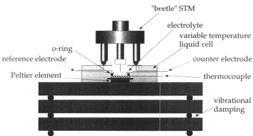
Fig.1. Schematicdrawing of the electrochemicaltemperature-variable STMsetup.
CH3(CH2)„_,SH
with n =6, 8,
10, 12, 14,
16 and 18. Fortheexperiments
carried out under
nitrogen,
thesamples
werekept
at 300 K for at leastone
day.
For the electrochemicalexperiments,
thefollowing self-assembly
programwas used: twohours 300
K,
twodays
ca. 325K,
thereafter several moredays
(or
inrare casesweeks)
300K.Allsamples
wereemersed,
rinsedwith ethanol and
quickly
used. STM measurementswereperformed
asde-scribed in
[29].
As shown inFig.
1,
a new feature is a Peltier element(operated
in theheating configuration)
that wecoupled
with a thin copperspacer to the bare side ofthe mica
sample,
thusattaining
a stablesample
and
electrolyte
temperature
(less
than 1 Kchange
perhour).
Thegold-covered sidewas incontactwith the
electrolyte,
50mMH2S04
(p.a.,
Fluka)
+ 0 or 1 mM
CuS04
(p.a.,
Fluka),
either in water(Millipore®)
or—
for the
high-temperature experiments
—
in 2:1
HOCH2CH2OH
(1,2-ethandiol,
ethylene glycol,
p.a.,Fluka): H20.
Ethylene glycol
veryeffectively
stops
the otherwisequick
evaporation.
The reference was a copperwire,
etchedin
HN03
and rinsed withwatershortly
before use.Thesample
wasmountedin a PCTFE STM cell
equipped
with a Ptcounter electrode. For the XPSsample
preparation
as well as for the redoxpair
measurements,exactly
the sameset-up
wasused. The redoxelectrolytes
containedRu(NH3)6Cl3 (Alfa)
orK3Fe(CN)6 (MicroSelect,
Fluka)
with KC1(p.a.,
Fluka)
and HC1(p.a.,
Fluka)
inethylene
glycol/water,
andanAg/AgCl
referencewasdipped
intothe STM cell. All
potentials
arequoted
withrespect
to the Cu/Cu2+pair
in 1 mM Cu2+(i.e.
0 mV read +250 mV on the standardhydrogen
scale and+50mV on the
Ag/AgCl
(KC1 sat.) scale).
Wealways employed
an EG&GPAR 400
potentiostat.
Thepotential
range above 500mV and below —200 mV wasusually
not accessed in order to avoid oxidation andim-Copper ElectrodepositiononAlkanethiolate Covered Gold Electrodes 111
ages are shown derivatised: steps
descending
from lefttoright
show up asblack
lines,
ascending
ones as white lines. TheX-ray photoelectron
spectrahave been
performed
in a VG ESCALAB 220. After removal from theliquid
we mounted thesamples
with electrical contactand introduced them via a fastentry
lock into the vacuumsystem.
In order to minimizeX-ray
tube induceddamage
thespectrometer
transmission was maximized withlowest
angular
resolution andanoverall energyresolution of 1.4 eVFWHM onthe Au4f7/2
peak
at84.0eVbinding
energy. TheX-ray
twin anode thatprovides
non-monochromatizedMg
Ka(1253.6 eV)
radiationwas retractedand run with 140W
input
power. Withrespect
to the maximum flux thesesettings
lower theresulting
electron flux from an aluminumsample by
afactor of0.3 to 15 nA/cm2. The emission
angle
was 0°(normal emission)
and 80°
(grazing
emission).
Fromthecomparison
ofthetwoemission direc-tions the vertical structure of the chemicalcomposition
of the(Cu)/
CH3(CH2)„_,S/Au(lll)
system
canbe inferred.3.
Alkanethiolate
layers
onAu(lll)
Inorderto
develop
abasis forunderstanding
thecomplex
copperdeposition
process we shall herepresent
studies of alkanethiolatelayers
onAu(lll)
under vacuum, in
nitrogen,
air and immersed inelectrolyte,
all in absenceof copper.
3.1 Structure and
morphology
Let us first focus on the chemical
composition
of alkanethiolatelayers
onAu(lll)
which can be detected with XPS. InFig.
2 the overview spectrumof
CH3(CH2),7S/Au(lll)
(sample
A)
is shown for normal emission. Thespectrum is dominated
by
the strongemission from thegold
substrate and the C Ispeak.
It can be seen that thesamples
remain almost oxygen freealthough they
have beenexposed
to air formore than 100s. In alldetails,
such a
spectrum
istypical
of thethiolate/gold
system[46, 47].
In
Fig.
3 the Au4f,
CIs,
O Is(and
forcomparison
Cu2p3/2)
XP spectraare shown for
sample
A. The Au4f7/2
peak
is set to 84.0eVbinding
energy. TheC Ispeak
is foundat 285.0 eV andcorresponds
tothat ofpolyethylene
chains[48].
We show aswell thespectra
fromgrazing
(80°)
emission(data
for carbon and oxygen are not shown since the
sample
holder contributesto the oxygen and some of the carbon
emission).
As theintensity
fromsulphur
(not shown),
theintensity
of thegold signal
isstrongly suppressed
;this is observed in presence
(as
inFig.
3)
and absence(not
shown)
of copper. The attenuationby
more than one order ofmagnitude
canonly
beexplained by
alayer
model in which the thiolate covers thegold
and binds-1-1-1-1-Au 4) SampleA Au4d Au4f Au4p Cu2p 01s , CuLMM
-~U,
1000 800 600 400 200 0ElectronBindingEnergy (eV)
Fig.2. Normal emission XPS ofaC18thiolatelayeron Au(lll); X-ray source Mg Ka.
Sample Acorresponds to an untreatedsample, while on sample B copper was
electro-chemicallydeposited.
In
Fig.
4 thegrazing
emissionintensity
of the CIs,
the Au 4fand the Cu2p3/2
levelareshownas afunction of exposure timetotheX-rays.
While the carbon emission remains constant, thegold
and the copper emission increase with the exposure time. Forsamples
without copperdeposit
we doobservethesame
aging
kinetics(not shown).
This variationclearly
indicates achange
ofthesample.
Theoverlayer
appears to become moretransparent
tothe emission from the substrate. The
gold
andcopperintensitiesperfectly
fitafirstorder kinetics ansatz I «(1
—
ße~"T)
where
ß
> 1 isasensitivity
factor and where x is the time constant. Within the
uncertainty
of thedata,
the
sensitivity
ß
and the time constant x areindependent
whether copperhas been
deposited
on thesample
or not. Thesensitivity
ß
is 0.45 ±0.07 for copper andgold,
x isinversely proportional
to thesecondary
electron flux from thesample.
From the value of x of 2•
104s and the
secondary
electron emission flux we find that the
secondary
electron currentdensity
from an aluminum
sample
times the time constants is in the order of 2• 1015 e"/cm2. This indiates that the thiolate films arevery
susceptible
toionizing
radiation as alsoreported by
Jäger
etal.[49]
(other
groups foundmuch
larger
timeconstants[50]).
Turning
the attention towards the interfacial structureprobed by
STM,
let us first note that thetunnelling
currentsemployed
(some
tenths ofnA)
are
essentially
sensitive tothesulphur
atom—
the
tip easily
penetrates
the thiolate chains which cannot offer local electronic states in the properCopper ElectrodepositiononAlkanethiolate Covered Gold Electrodes 113
(Fig.
5),
can thus be ascribed tothesulphur
atoms,yielding
a coverage of0.33. Note that thesamestructurewas found fora
sulphide
adlayer
adsorbed on anAu(lll)
electrode and forS/Au(lll)
in vacuum[7].
However,
we detected'super-superstructures',
e.g. the well-known centered(4X2)
distri-O) 'c 3, c O)
J:
0 0 10 20 30 40X-ray
exposure-t¡me(103
s)
Fig.
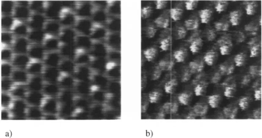
4. Grazing photoelectron emission intensities ofC Is, Au 4f and Cu 2p3/2 (C18 thiolate)as afunctionofexposuretotheMgKoX-raysource.The solid lines in the data of copper andgoldarefitsto first order kinetics.a)
b)
Fig.5.Molecular resolution STM
images
takeninnitrogenshowing
thec(4X2)pinwheel
(a)and thec(4X2)zig-zag
(b) superstructureson aC,0thiolatesample. Tunneling
param-eters: (a) I = 1.0nA, V = 1000mV; (b) I = 0.6nA, V = 1000mV Image size:
3.5 nmX3.5nm.
bution
(Fig.
5)
of the(73
X73)R30°
elements(in
proper notation(3X273))
[10, 52-55].
At lower coverage(attainable
by
vapourphase
dosing
of thiols[56]
orby
heating
above 370K[57, 58])
and for shorti i i
i-C1s
CopperElectrodepositiononAlkanethiolate Covered GoldElectrodes 115
Fig. 6. STMimageofaC10thiolate-covered Au(Hl)surface in air. The dark linesare
thiolate domain boundaries which are pinned by the substrate vacancies (dark spots). Tunnelingparameters: I = 0.3nA,V = 900 mV. Image size: 320nmX320nm.
chain thiolates we detected
striped
structures[58]
(see
also[56,
57, 59,
60]).
Allthese structurescanexist in different domainsseparated by
domainwalls. These walls show up as dark grooves of
roughly
half amonolayer
depth
and 1 to 3nm width. InFig.
6 the walls often extend betweenneigh-bouring
substrate vacancies(large
darkspots),
butthey
can also terminateat other walls or at
steps.
During heating
innitrogen,
the number of grooves in an STMimage
diminuishes,
i.e. the average domain size in-creases[61].
Further
healing
processes that can be followed involve Ostwaldripen-ing,
coalescence and annihilation(at
steps)
ofthe vacancies[43, 45].
The latter are ascribed toetching
processes[62, 63]
and thelifting
of theAu(lll)
reconstruction and concomitant surface diffusionduring
theself-assembly
process[64, 65];
their surface is coveredby
thiolate as are allotherterraces
[58,
66,
67].
Our latest
experiments
show that the(73
X73)R30°
lattice,
domain walls and vacancies arefoundalso when thesamples
areimmersed inelec-trolyte
andkept
underpotential
control(in
situSTM).
When we use themodified
electrolyte
basedon anethylene
glycol/water
mixture,
we can nowadditionally
scanthe surface at elevatedtemperature
[28].
As visualized in theimage
series ofFig.
7,
depicting
a vacancy that israpidly
filled withmaterial from a
nearby
step, we foundhighly
mobile surfacesalready
at 335 K. The surfaceappeared
to be moremobile than innitrogen, probably
a result of the electrochemicalpolarization.
Some further
properties, especially
theability
to transfer electronsthrough
athiolatelayer,
canbeprobed
withcyclic
voltammetry.
Aselectro-lytes
weroutinely
usedsulphuric
acid either inwater orinethylene glycol/
water. In
passing
we note thatweproved
thatethylene glycol
does neitheraffect the
electrochemistry
ofthiolate/Au(l 11)
nor that of the copperre-ductionat
thiolate/Au(l 11)
and bareAu(lll) [28].
Thevoltammograms
aretypical
for nonreactive surfaces since the doublelayer
current is smaller than forabare metal surface. Ingeneral,
the currentfor short chain thiolatesis
larger
than forlong
chain thiolates. Athigher
temperatures
the current risesconsiderably.
Thus electrons canbe transferredacrossthe thiolateeas-ier when the chain is short and the temperature
high.
However,
one shouldkeep
in mind thatthe doublelayer
could have a structure andthuscapacity
differing
from thaton baregold.
Hence we also
probed
the surfaces with a redoxpair, Fe(CN)s/4".
Thevoltammogram
inFig.
8 reveals thetypical
current waves that result fromkinetic and diffusional
limitations,
but with lesspeak
current than on bareAu(lll).
Wefound the samebehaviourasfor the doublelayer
currentmen-tioned above: the redox waves' current rose at
high
temperatures
and for short chainlengths.
Note that thetemperature
behaviourcan be morecom-plex
[68].
Experiments
withRu(NH3)i/2+
normally
showed a muchhigher
current ;
however,
thesamedependence
onthe thiolate chainlength
is found(Fig.
9).
To assess thefindings
we note that the diffusional limitation mustbe the same at bare and thiolated
Au(lll).
The rate of the slowest(rate
determining)
processresponsible
for the thiolates'blocking
behaviour canbe the
charge
transfer across the thiolate orpossibly
apenetration
of thecomplexes
into the thiolate.In the
following,
we shallinterpret
the structure andmorphology
of alkanethiolate-coveredAu(lll)
at 300K. We will progress from asingle
molecule
(sub-nm)
to themesoscopic
scale(pm).
First,
ourXPS datacon-firm the
accepted
structure model of agold
surface coveredby
sulphur-bound thiolates. The small oxygen contamination is
likely
due toairexpo-sure. It may consist of adsorbed oxygenatoms
(e.g.
atthiolate-freedefects)
and/orwater(difficult
toremovecompletely
invacuumchambers).
However,
oxygen isaminor
species
on athiolatesurface,
evenafter exposuretoair.Fig.7.In situelectrochemical STM imagesequence(time separationca. 1 min)
showing
the temperature induced
mobility
ofaC6thiolate/Au(lll) interfaceat335 K.Electrodepotential:
300 mV vs. Cu/Cu2+, i.e.positive
from the UPD range, thus the surface iscopper-free. Electrolyte:
50mM H2S04 + 1 mM CuS04 with the solventbeing
a 2:1mixture ofHOCH2CH2OH:H20.Tunnelingparameters:I =0.5nA,V = 120 mV.Image
CopperElectrodepositiononAlkanethiolate Covered Gold Electrodes 117
a) 100 -, 50
"s
< ° 3. '" -50 -100 b) 1 0 CM B -1 U < -2 3. - -3 -4 -5 O 200 400 E(mVvs.Cu/Cu2+)Fig.8.Cyclic voltammograms foranAu(lH)electrodeat 300K(a),foraC16
thiolate-coveredAu(lll)electrodeat300 K(b,dashedline)andat335 K(b,solidline).
Electro-lyte: 1000mMKC1+ 1 mMK,Fe(CN)6with the solventbeinga2:1 mixture of HOCH,
CH2OH:H20. Scanrate: 50 mV/s. Potentials weremeasured vs.the
Ag/AgCl
electrodeand are reported vs. a hypothetical Cu/Cu2+ (1 mM) reference electrode for an easier
comparison
with thepreviously
shown voltammograms.Extending
the view from asingle
moleculetoneighbouring
molecules,
we notethat the coverage ofsulphur
atoms(and
thusof thealkanethiolates)
is in most cases
1/3;
thesulphur
atoms occopy a(73
X73)R30°
lattice(see
above).
Exceptions
are encountered for the short-chain thiolates(e.g.
n = 6 where this lattice and astriped
structurecoexist)
or for the lowcoverages attainable either for
samples
annealed above 370 K orby
vacuumdeposition
of thiols. As wealready pointed
out in section1,
the(73
X73)R30°
geometry
is also found for theS/Au(lll)
system.
This and other(quasi)hexagonal
structures(e.g.
found when soft bases are adsorbedat noble metal surfaces; evenwhen the substrate structureis not
hexagonal
[1, 2])
aretypical
for abalance betweenadsorbate-substrate andadsorbate-adsorbateinteractions.
Clearly,
this balance has to beadditionally
affected whenalkyl
chains interact with each other. It is well known that this results in the all-transCopperElectrodepositiononAlkanethiolate Covered Gold Electrodes 119
_I_I_I_L
-300 -200 -100 0
E(mVvs.Cu/Cu2+)
Fig. 9.Cyclic
voltammograms
for a C10thiolate (solid line) and a C,4thiolate-covered(dashed line) Au(lll) electrode at 300K. Electrolyte: 50 mM H2S04 + 1 mM Ru(NH3)6Cl3. Scanrate: 50 mV/s. Potentials were measured vs. the Ag/AgCl electrode
and are reported vs. a
hypothetical
Cu/Cu2+ (1 mM) reference electrode for an easiercomparisonwith the
previously
shown voltammograms.| Au OS • C
Fig. 10. Models ofthe CH3(CH2)9S/Au(lll) interface: (a)
alkyl
chains in the all-transconformation,(b) alkyl chainspartially ingaucheconformation.
configured alkyl
chainsbeing
tilted away from thesurfacenormalby
about 30°(see
Fig. 10(a)).
The azimuthal tilt direction lies betweenthe directions of the next and nearest nextsulphur neighbours.
The above-mentionedc(4
X2)
lattice appearstobe basedon anordereddistributionofalkyl
chaintwist
angles (presumably
a twist around the S—Caxes);
structures basedonordered distributions of
alkyl
twistangles
exist also in bulk alkanes[4].
60%
o < 3 -60 -120 -180We can conclude that the thiolate structure is based on the strong Au—S
bond;
the maximum coverage isgoverned by
S —S and interchain interac-tions—
each one exhibits an energy
minimum,
and theirinterdependence
yields
an overall minimum with theoptimum
geometry
described above.The
densely spaced alkyl
chains form an effective spacerlayer
that blockselectron transferas evidenced
by
the voltammetric data.On the
length
scale of 10nm,we find the groovesthatform thebound-aries between
differently
oriented molecular domains.Unfortunately,
it isimpossible
todeducea structural model for them:firstly,
the mechanism oftunnelling
on thiolates is still underdebate,
hence thedepth
is difficult tointerpret; secondly,
molecular resolution of the grooves is very difficult. Thesimplest
idea is anantiphase boundary
where the S —S interdomaindistance is
larger
thanthe intradomain distance of7?
atomicgold
distances,
but also
missing
rowsof thiolate molecules have beensuggested
[55].
Finally
let usshortly
focus on themesoscopic
scale(pm):
this is thetypical
length
ofgold
substratesteps.
Very
long
andstraight
steps
arepre-sumably
due to thehealing
of volume defectsduring
thegold
flamean-nealing (gliding along
internal(111)
planes);
hencethey
can cross eachother. Shorter and more round
steps
shoulddevelop
viatransport
processesduring
gold
flameannealing
andquenching.
3.2 Thermal
dynamics
Substantial
changes
of the surfacemorphology
manifest themselves instep
movements whichcanbe ascribedtothe diffusion ofgold
adatomsorsingle
atom vacancies. Indeed we use the
smoothening
effect ofsurface diffusionin both the vacuum
heating
and flameannealing processing
of ourgold
samples.
Naturally,
such processes arethermally
activated. Onthiolate-covered
Au(lll),
theirrate is muchhigher
than on bareAu(lll)
since theAu—Au interaction is weakened
by
thestrong
Au—S bond. Substrate atom diffusion was also recorded forsimilarly
strongly
boundhalogen
atoms onAu(100) [69a], Au(lll) [69b], Au(110] [70]
andPt(110) [71, 72].
High
temperature
dosing
ofhalogènes
can evenproduce virtually
defect-freesur-faces
[2, 73]
as canprolonged annealing
of thiolate-coveredAu(lll)
[42].
For this
annealing procedure,
the vacancies andstep
edges
moveby
dif-fusion of
single
substrate atom vacancies[26, 45].
This leads to Ostwaldripening
before the vacancies reach each other(vacancy
coalescence)
andfinally
othersteps
(vacancy annihilation).
We can group all such events under theheading 'strongly
activated': thethermodynamic driving
forceshave to be so
large
thatthey
result indesorption
of moreweakly
boundadsorbates. An
example
for adriving
force is thetemperature
that shouldbe above ca. 800 K for
gold
flameannealing
(acting
to desorbimpurities
andresulting
inlarge
scalestep
movements)
oraboveca. 340 K for vacancyCopper ElectrodepositiononAlkanethiolate Covered Gold Electrodes 121
Another
example
for'strong
activation' is the electrodepotential;
changing
it to either morepositive
or morenegative
values can result indesorption
of adsorbed substances and surface diffusion. In most cases, anelectron is transferred from orto the adsórbate
during
thedesorption. E.g.
only
below -1100 mV thiolates desorb fromAu(lll) [74, 75],
demon-strating
thatthey
bindstrongly;
below—
500 mV
sulphide
desorbs fromAu(lll) [7];
below —300 mV iodide desorbs fromPt(110),
causing
surfacemass
transport
of the substrate[72]
; —200mV sufficetodesorb the weakerbonded
sulphate
ionfromplatinum
surfaces[76]).
In thepositive potential
range, the situation can be muchmorecomplex;
often an adsórbate is firstoxidized and the
product
candesorb,
e.g. alkanethiolates are oxidized toalkanesulphonic
acids. In any cases,changing
thepotential
willsupply
theCH3(CH2)„_,S/Au(lll)
interface with additional electrons(or
draw elec-trons fromit)
andthereby
weaken the Au—Au and Au—S interactions. The firstcaseleadstosubstratemobility,
the lattertoadsórbate surface diffusionor
desorption.
However,
theanalogy
tohalogenide
orsulphide
adlayers
reaches itslimits when we consider that in the course of surface diffusion not
only
Au—Au,
Au—S and S —Sinteractions,
but also interchain forces come intoplay. Clearly,
forlonger
alkyl
chainsthey
arelarger
and present anad-ditional
barrier;
hence the mobilities will be lowered(as
observed[43]).
Whether thiolate molecules remain bound to amoving
gold
adatom ornot,during
a diffusion event interchain van-der-Waals bonds are broken andreestablished. Thus the thiolate has toreorient which canentrain formation ordestruction of the all-trans conformation and
change
of azimuth and twistangle.
At
temperatures
above ca. 330K,
alarge
part
of the thiolate moleculesmay exist in an
energetically (slightly)
disfavoured state such as distorted twistangles
orgauche
conformations; thesulphur
atoms remain in a fixedposition.
Let us name such a situation'moderately
activated'.Locally
theeffective thickness will be
lowered,
i.e.'spots'
appear in the otherwise dense 'forest' ofalkyl
chains(see
Fig.
10(b)).
Such'spots'
are not to be confused withmissing
molecules(which
are rare iftheself-assembly
wasgiven
sufficienttime).
Here an ion in theelectrolyte
canapproach
thegold
surface much more
closely.
It canthereby
at leastpartially
penetrate
thethiolate,
facilitating
anelectron transfertoorfrom thegold
surface. For this reason we detecthigher
doublelayer charging
or redox currents when weincrease the
temperature.
The currents also increase when we use shorteralkyl
chains—
in thiscase,the molecular spacer
layer
becomesthinner,
andanioncan
(even
withoutpenetration) approach
thegold
surfacemoreclose-ly
than in the case oflong
chains(see
Fig.
9).
We note that'moderately
activated' processes cannot bebrought
aboutby potential changes
—
this
-100 0 100 200 300 400 E(mVvs.
Cu/Cu2+)
Fig.11.Cyclic voltammogramsforCl()thiolate-coveredAu(l 11)at300K(a) and 335 K
(b)
showing
the temperaturedependent
blocking behaviour towards copperdeposition.
Electrolyte:
50mM H2S04 + 1 mM CuS04 with the solvent being a 2:1 mixture ofHOCH2CH2OH:H20. Scanrate: 10mV/s.
500 mV and -200
mV)
without noticeablechanges
of surfaceproperties.
In otherwords,
in this range theCH3(CH2)„_,S/Au(lll)
system
isideally
polarizable.
4.
Copper electrodeposition
on
alkanethiolate-covered
Au(lll)
4.1 From UPD islands to OPDlayers
We
begin
thepresentation
of the copperdeposition
studies with the voltam-metricexperiments.
Herevoltammetry
is notsimply
ananalytic
tool,
butalso the methodtoachieve
potential
control of thesystem
(for
the STM and XPSexperiments,
we started at apotential
of 400 mV where copperde-posits
neither on bare nor on thiolatedgold,
then lowered thepotential
insteps
of20,
50 or 100mV).
The
voltammograms
of thiolate-coveredAu(lll)
samples
in contact with Cu2+ inelectrolytes
basedonwateraswell as onethylene glycol/water
areusually
featureless with low doublelayer charging
currents(see
Fig.
11).
CopperElectrodepositiononAlkanethiolate Covered Gold Electrodes 123
In the UPD
regime,
i.e. above the Cu/Cu2+equilibrium potential
of0mV,
no features were found
either,
albeit in some cases very shallowpeaks
as-signed
tocopperUPD showed up. This behaviour reflects acertainsample-to-sample variability
of thiolatelayers
as alsoreported by
other groups[24, 77].
Below 0mV the currentdrops slightly, pointing
towards copperdeposition
at amuch reducedratecompared
to a baregold
substrate wherecurrents
drop
toseveral tenpA/cm2
(compare
e.g. thecurrenttransients for copperdeposition
onAu(lll) [78, 79]).
Rising
thetemperature
increasesthe double
layer
current and reveals small UPDpeaks
for allsamples
(see
Fig.
11).
A reasonableexplanation
is thehigh
temperature
defect structure of the thiolate(see
section3.2)
that should accelerate the reduction of Cu2+. Faradaic andcharging
currents also increase withdecreasing
thiolate chainlength.
Thesefindings
compare well with the behaviour incopper-free
elec-trolytes
(see
section3.1):
higher
temperatures
and shorteralkyl
chainsgen-erally
increase the current, whether it is due tocharging
or Faradaiccur-rents
—
in both cases electrons have tobe transferred
through
the thiolate to theadjacent electrolyte phase.
After
regulating
thetemperature
andsetting
thepotential
to a fixedvalue,
the surface structure can be followed time resolvedby
insitu STM.We now have to consider three
parameters
influencing
themorphology:
temperature,
potential
and thiolate chainlength.
In a certain range of theparameters
(UPD
for all thiolate chainlengths
andtemperatures; OPDonly
forn > 12 at lowertemperatures,
seeTable1)
thesystem
showed asurpris-ing
topography:
monolayer
high1
islands with an average diameter of2nm cover10to 15%of the surface(Fig.
12).
They
arerandomly
distributedandalso found in the substrate
vacancies;
they
are notpinned
atsteps
or at domain boundaries. The initial nucleation of these islands couldnotbe fol-lowed. Furthergrowth proceeded
eithernot orextremely slowly
atless than 0.7 nm in two hours.Apart
fromthe fact that island formation in the UPD range is a rarephenomenon
(but
see[37]
and[38]),
the observed islandshave the
unique
property ofchanging
neither size norshape
forhours,
i.e.they
cantruly
be addressed as stable or at least metastable nanostructures.At all other conditions
(OPD
forn < 12and OPD for all n at 345K)
apseudo-layer-by-layer growth
was found(Fig.
13):
islands grow untilthey
coalesce.
Only
islandsalready
nucleated in theUPDregime
grow,nofurtherislands nucleate. In electrochemical terms, the nucleation is
instantaneous,
not
progressive,
in contrast to copperdeposition
on bareAu(lll) [79].
When a
monolayer
is almostfilled,
the nextlayer
nucleates ontop.
How-ever, the
growth speed depends strongly
on thetemperature
and the chainlength.
At 300K,
even the shortest chain(n
=6)
system
exhibits a veryslow
growth
(at
least onehour perlayer).
Athigh
temperatures,
all thiolatelayers
allow arapid growth
in the range of minutes perlayer.
1
The
monolayer heights
of Au(lll) (0.236nm) and Cu(lll) (0.208nm) are too similartobedistinguishedinourSTM setup.Table 1.Copper growthscenarioasfunction of alkanethiolate chainlengthn,temperature
and
deposition
potential range(OPD: <0mV,UPD: >0mV).room temperature elevated temperature short chain UPD 2D islands OPD layer-by-layer UPD 2D islands OPD layer-by-layer
long
chain UPD 2D islands OPD 2Dislands UPD 2D islands OPD layer-by-layerFig.
12.In situ STMimage showing
the 2D copper island formation ona C,8thiolate-coveredAu(lll)surface in theUPDrange. Electrolyte:50 mMH2S04 + 1 mMCuS04.
Electrodepotential:30mVvs.Cu/Cu2+.Tunnelingparameters:I=0.3nA,V= 200 mV.
Image size: 220nm + 220nm.
For a
special
set of theparameters
(short
chainthiolates,
300K,
OPD)
we observed a fractal
shape
of thegrowing
andcoalescing
islands asvisualized in
Fig.
14: each islanddevelops
three 'arms' which canagain
sym-Copper Electrodepositionon Alkanethiolate Covered GoldElectrodes 125
Fig.
13. In situ STMpicture exemplifying
the OPD copperlayer-by-layer
growthon aC,othiolate-covered Au(lll) electrode at 300 K. Electrode potential: -90mV vs. Cu/
Cu2+. Electrolyte: 50 mM H2S04 + 1 mM CuS04. Tunneling parameters: I = 0.4nA,
V = 110mV. Image size: 220nmX220nm.
metry
of theunderlying gold
surface and/ortothesymmetry
of thesulphur
adlattice. Suchgrowth shapes
areusually
associated with akinetically
hin-dered
growth
[80].
To obtain information onthe chemical
composition
of theinterface,
weemersed
C18
thiolatesamples
on which copper had beendeposited
for 3 hat50or20mVat300
K,
i.e.samples
coveredby
copper islands.They
wereinvestigated
with XPS. The overviewspectra
(see
Fig.
2,
sample
B)
show the same featuresas in absence of copper, butadditionally
a Cu2pV2
emis-sion is
present
(correspondingly
thegold
emissiondecreases).
Intensity
curves
(Fig.
4)
indicate arapid
destruction withX-ray
exposure. Theoxy-gen contamination is
slightly higher
than for thecopper-free samples,
but stillcorresponds only
to a minorportion
compared
to that of copper. From theintensity
ratio,
thephotoemission
cross sections and thebinding
energyof Cu
2p3/2
(932.1 eV)
weconclude that thedeposited
copper didnotoxidizealthough
thesamples
had to endure more than one minute of contact withlaboratory
air which should suffice forcomplete
oxidation ofa coppersur-face. Hence the copper is
protected against
oxidation. In addition to theFig. 14. In situ electrochemical STM image of fractal islandsthat nucleated during the
growthof thefirstcopperlayeron aC6thiolate-coveredAu(lll)electrodeat300 K. The
imagewasobtained after80min of OPDpolarizationat —110mVvs.Cu/Cu2+.
Electro-lyte:
50mMH2S04 + 1 mMCuS04.Tunneling
parameters: I = 0.5 nA, V = 120mV.Image size: 175 nmX175nm.
grazing
emission(see
Fig.
3).
Thisemphasizes
that the copperpenetrated
the thiolatelayer
during
thedeposition.
4.2 Structure of
electrodeposited
copperThe formal electrode
potential
(measured
here with the Cu/Cu2+ referenceelectrode)
wequoteisnottheoneofthethiolate/electrolyte
interface. Hencetheoretically
one cannotexpect
a copper bulkdeposition
at 0 mV(even
athighest
Cu2+concentrations).
However,
thepotential
drop
in the thiolatelayers
should not exceed 100 mV since theoverpotential
for copper bulkdeposition
of about 150 mV is the same as on bareAu(lll)
andAu(100)
[18].
The reduction of Cu2+ in acidic mediaproduces
copper metal. In our case it grows inislands,
and the firstquestion
wehave toposeconcerns thecopper islands' distance from the
gold
surface. Wealready
disproved
the idea of copperresiding
inthiolate-free surface areas[29]
since such areaswould result in clear
Cu/Au(lll)
UPDpeaks
for allsamples.
Fig.
15 illustrates the two furtherprincipal possibilities
that arise:first,
the copper islands could be located between thiolate andgold
(CH3(CH2)„_1S/Cu/Au(lll)),
second,
they
could be ontop
of the thiolatelayer
(Cu/CH3(CH2)„-iS/Au(lll)).
We here discard other models becauseun-Copper ElectrodepositiononAlkanethiolate Covered Gold Electrodes 127
H
Au B Cu os • cFig.15. Schematicrepresentationof the
possible
structures oftheCu/thiolate/gold inter-face: copperelectrocrystallized below(a) and above(b)the thiolate layer.likely (e.g.
alloying
into thegold
surface that isonly
known for the(110)
face
[81]).
The second model wouldpostulate
isolated copper islandscon-nectedtothe
methyl
end groups(see
Fig.
15(b)).
Aswealready pointed
out[27],
onemight
think that the necessary electron transfer to thetop
of the chains shouldnicely explain
theslow formation(but
seesection 4.4!).
How-ever, several
arguments
speak against
the model: ifone observesUPD,
thegrowing
metal should have astronger
interaction with the substrate thanwith itself. Forcopperontopof the thiolate
layer,
thisisimpossible
becausethe Cu-H
(or Cu-CH3)
interaction is very weak. The islands evenwith-stand
rinsing
with water, i.e.they
arestrongly
bound.Also,
heating
involv-ing
the formation ofalkyl gauche
defects should shortensome(but
not all!)
of the thiolate chains below an island. Then the island that behaves as a
rigid
copperlayer
'disk'(compared
to the thiolatelayer)
would remain attachedonly
to the intactthiolates,
but the distance to thegold
surface would be the same as at lowtemperature
(when
all molecules areintact).
Hence the electron transfer
probability
would be the same at low andhigh
temperatures,
and copper shoulddeposit
at the same rate; this is not ob-served.Furthermore,
let us assumean island thatadditionally
has somecontacttothe substrate
(i.e.
a copper columnthrough
thethiolate).
Such an islandof copper atoms
should,
in absence ofstrongly
bound coadsorbates(S02~
does not
qualify!),
continueto grow 3D[22]
asCu/Au(lll),
in contrastto the observations.Clearly,
if the thiolatelayer
isdamaged by large negative
Copper placed
below the thiolate(Fig.
15(a))
is in accordance with thefollowing
facts:firstly,
the XPS data show anangular dependence
of theCu
2p
emission whichmustbe due toconsiderable amountsofmaterial,
i.e. thiolatemolecules,
ontop
of the copper.Secondly,
theresulting
Cu—S bond isstrong
andcaneasily explain
thepassivation
ofcopper[29]
:it isimpossi-ble to rinse off the
islands,
they
withstand verypositive potentials,
copper doesnotreactwith air which wouldproduce higher
Ols XPSsignals.
Note that suchathiolate/copper
structurecan be called acoadsorption
structure,and
examples
likeI/Ag/Pt(lll),
detected afterelectrodeposition
of silveronI/Pt(lll) (not
adsorption
of iodide onAg/Pt(lll)!)
are well documented[33, 34, 73].
Thequestion
we haveto address is whether copperatoms canpenetrate
a thiolatelayer;
in section 4.4 we will show that this is indeedpossible.
Here we mention that silverevaporated
onthiolate/Au(l 11)
in vacuum has indeed been observed topenetrate
thelayer
[11, 82].
Let usalso mention that thiolates
readily
adsorb onCu(lOO) [83]
and that evenmultilayer
copper thiolates can form[84].
All thesearguments
lead us to propose aCH3(CH2)„_,S/Cu/Au(lll)
structure.Further structural details are much more difficultto observe. This con-cernsthe lattice of the copperatoms which could be
(1
X1)
asinacomplete
UPD
layer
[15, 85, 86],
ahoneycomb (73
X73)R30°
lattice as in theincomplete
Cu +SOJ"
coadsorption
UPDlayer
onAu(lll) [14, 86-88]
or a normal(73
X73)R30°
structure. All three would offer reasonableadsorption places (e.g.
hollowsites)
for thesulphur
atoms. A more intricatefeature is the structureof the islands' rims. Hereone could
probably
find atopography
that isdistinctly
different from that in the island—
thusonemay
explain
thesurprising
stop
ofgrowth
and hence the instantaneous instead ofprogressive
nucleation. Since this isonly
the case forlong
thiolate chains and lowtemperatures,
we canspeculate
thatespecially
thealkyl
chainsadjust
themselves inaspecial
structure.However,
STM observations(which
for the currents we
employed probe
thesulphur
atoms rather than thechains)
didnotyield
anyclues.4.3 Thermal behaviour
For an
interpretation
oftemperature
phenomena
we have to consider thechanges
thatdevelop
in the thiolatelayer during annealing.
Thegradual
development
of thiolate defect structures such asgauche
conformations,
newtwistangles
orpossibly
azimuthal disorder(see
section3.2)
willagain
allow for
increasing penetration
ofions2,
this timeincluding
Cu2+. As forFe(CN)6~,
a reduction will occur much faster.Doubtlessly,
thecomplete
penetration
is now even more facile.However,
we also have toexplain
aqualitative change:
islands grown on thiolates of all chainlengths
canco-2
On the fate ofthe
hydration
shellwecanonly speculate.This iseventrueinabsence of thiolate [89]!Copper Electrodeposition onAlkanethiolate Covered Gold Electrodes 129
alesce at
high
temperatures.
This means that the unknown barrieragainst
further
growth (presumably
atthe islandrim)
is overcomeby
thermalacti-vation. The
pseudo-layer-by-layer growth
is duetothepresenceofthe thiol-atewhichalways
staysontop; otherwisethegrowth
(on
purecopper)
would carry on much faster and 3D nodules would result. This is the classicalpicture
ofa surfactantthathinders thegrowth
in the directionnormaltothesurface as also observed whencopper was
deposited
ongold
in presence ofcrystal
violet[20].
However,
our surfactant is adsorbed in awell-charac-terized
geometry
and will neither desorb nor readsorbduring deposition.
Thusweexcludeoneof the many processes that
complicate
theunderstand-ing
of surfactant action inelectrodeposition.
At
high
temperatures
substratesteps
becomemobile('strong
activation',
see section
3.2).
Whenweaccept
that copper is boundtothe substrate(see
section
4.2),
copper island rims — copperstep
edges
—should be at least
as mobile as the substrate
steps.
This isequivalent
to an incrased islandperimeter mobility,
i.e. the fractal islandshapes
transform tocompact
shapes.
Obviously,
the barrieragainst
furthergrowth
thatprevails
at lowtemperature
is overcome, and furthergrowth
and coalescence can occur.This
arguments
are in line with thetheory
of surface diffusion limitedaggregation
that hassuccessfully
beenapplied
toexplain
ramified metal islands grown in vacuum.However,
the fact thattemperature
alsoenhances copper
penetration
and thusdeposition
rate makes aquantitative
theoretical
modelling
verydifficult,
sincetwointerdependent
barriers(thiol-ate
penetration
and the barrier at the islandrim)
are overcome at the sametime.
4.4 Potential
dynamics
—copper
deposition
ratesWe shall start the discussion with a look at the
permittable
limits of thepotential.
At thepositive
end,
we dissolve the copper islands atpotentials
several hundred mV
positive
of the Cu/Cu2+equilibrium
value. Note thatwe haveto wait several hours at 400mV
(300
K),
and some islands resistdissolutionevenat1000mV
[29]
whichimpressively
demonstrates thepas-sivation. As one
expects,
the dissolution is much faster when thetempera-ture is raised.
Inthe cathodic
regime, only
wellbelow —200 mV thelayer growth
canchange
to 3Ddeposition
of nodules with diameters above 100nm. Sincevoltammograms
show copper UPDpeaks
after suchnegative
excursions,
some bare substrate
spots
appear to exist which wouldclearly
cause theobserved
growth
oflarge
nodules.Forthe UPD processes, nocurrent flow is found since the
growth
is soslow that the
resulting
peaks
would be far too shallow(sub-nA
range).
In the OPD range, the detectedcurrentsusually
predict
adeposition
ofamono-layer
of copperduring
several minutes which is
-at 300 K
than observed
by
STM. Thediscrepancy
canbeexplained by
the destructionof the
sample
close to the vitonring
where weoccasionally
found visiblecopper
deposits;
this means that copper had heredeposited
at least 100 times thicker than elsewhere. Thus theglobal
current is unreliable at least when its value is small. Therefore we estimate thedeposition
rate from STM measurements:typical
rates are 10% ofamonolayer
in one to twohours
(UPD),
onelayer
in twohours for copperlayer growth
on short andmedium chain thiolates
(OPD)
and onelayer
per minute athigh
tempera-tures
(OPD)3.
Assuming
a Cu(1
X1)
geometry
onAu(lll)
with amono-layer charge
of 440pC/cm2,
thisgives
rates of 0.01pA/cm2,
0.06pA/cm2
and 7pA/cm2,
respectively.
We can setlimitstotheexperimental
rates:0.005
pA/cm2
< r< 10pA/cm2.
(1)
In order toexclude or
verify possible
mechanisms,
it is instructive tocom-pare those rates to rates calculated under
typical
conditions. Let us first assume that bulk diffusion of Cu2+ is therate-limiting
(slowest)
process.Thenthe Cotrell
equation
wouldapply
[12]:
r, = 2
Fc0
JUhti
•[1
-exp
(2
FAE/RT)]
(2)
where F = 96485
C/mol,
D is the diffusionconstantof Cu2+ inelectrolyte
(5.7
• 10~6 cm2/s[90]),
c0 the Cu2+ concentration(1 mM),
t thetime,
R = 8.314
J/(mol
K),
AE thepotential
stepcausing
thedeposition
(e.g.
-100mV)
and T thetemperature.
Weshould then findr, « 260
pA/cm2
•JV(tIsj
(2a)
(comparison:
440pA/cm2
accounts fora Cu(1
X1)
monolayer
onAu(lll)
deposited
in onesecond)
which isabout 100 timeslarger
than the transient we observedduring
the first minute ofpolarisation.
This means that thediffusion isnot the
limiting
factor.This could leave the electron transferasthe slowest process. First let us
concentrate onthecase of copper
deposition
oncopper, e.g. copper islands.Then the slowest
possible
rateis thatat zerooverpotential
where dissolutionand
deposition
currents cancel each other. Theirvalue,
theexchange
currentdensity,
is[91]
r2« 500
pA/cm2
(3)
3
Theestimatesare rough, hence the copperatom