Anal Bioanal Chem (2006) 384: 47–49 DOI 10.1007/s00216-005-0143-1
T R E N D S
Jorge Pisonero
Glow discharge spectroscopy for depth profile analysis:
from micrometer to sub-nanometer layers
Published online: 19 November 2005
# Springer-Verlag 2005 Introduction
The growing industrial interest in new materials and their properties has resulted in the application of thin (μm) and ultra-thin (nm) coatings to more and more materials in different fields of technology (including thin film optical coatings used in reflection and glare reduction, addition of a decorative color, thermal control, wear-resistance and transparent electrical conduction; multilayer structures on silicon used in the manufacturing of semiconductor de-vices) in order to improve their quality and performance [1]. Moreover, most physical properties of thin films (cor-rosion resistance, adhesion, optical and magnetic proper-ties) are related to their chemical compositions and structures. In order to optimise these properties, adequate analytical techniques are required, since it is important to be able to measure film thicknesses and chemical param-eters with low limits of detection, good reproducibility, and high lateral and depth resolution.
Various analytical techniques are available for depth profiling, providing different abilities to analyze layers. For instance, depth profiling of the first atomic layers of a sur-face (sub-nanometer to nanometer scale) is usually ac-complished by Auger electron spectroscopy (AES) and secondary ion (neutral) mass spectrometry (SIMS) [2,3]. On the other hand, depth profiling of thicker layers (sub-micrometer to sub-millimeter scale) can be carried out by laser ablation-based spectroscopy [4].
However, among these techniques, the emergence of glow discharge (GD) plasma devices for practical thin film analysis should be highlighted. GDs are currently known as powerful analytical tools for performing depth profiling analysis of relatively thick films (in the tens of microns range), including galvanized or painted steels [5].
Howev-er, the analytical potential of GD devices for thin and ultra-thin film analysis (<10 nm thick) has been recently dem-onstrated [6,7].
Additional advantages of GD sources include high depth resolution (nm), fast sputtering rate (μm/min), multi-ele-ment capabilities, low matrix effects (multi-matrix calibra-tions), a well-established quantification method, low limits of detection (μg/g to ng/g), ease of use and high sample throughput. However, one significant drawback is the poor lateral resolution (a few millimeters).
Glow discharge spectroscopy for depth profile analysis
Glow discharges have found popular use as plasma sources in combination with optical emission spectrometry (OES) or mass spectrometry (MS) due to the ability of the plasma to generate atomic or ionic populations directly from solid samples. One distinctive feature of this technique is that the processes of atomization and excitation/ionization are sep-arated in space and time, explaining the low matrix effects observed in the source. Furthermore, the use of radiofre-quency (rf)-powered GDs instead of the traditional direct current glow discharge (dc-GD) has broadened GD ap-plications to the analysis of both conductive and noncon-ductive samples. More details about the fundamentals and applications of GD have been given elsewhere [8–11].
GD-OES is an extremely rapid technique for depth pro-filing that has shown its potential for the quantitative anal-ysis of many types of thin and ultra-thin films (organic coatings, electrodeposited films, and so on) [12]. In fact, the GD-OES technique is now recognized by standardiza-tion bodies and GD-OES equipment is manufactured by several companies (including HORIBA Jobin-Yvon, LECO, Spectruma Analityk). However, there are still some im-provements that need to be made to GD-OES:
Further research is needed in the area of quantification of coated glasses and ceramics (materials with many applications in optical coatings, biomaterials, and so on). Related to that, Fernandez et al have recently J. Pisonero (*)
Laboratory of Inorganic Chemistry, ETH Zurich, Hoenggerberg, HCI G141, Wolfgang Pauli-Strasse 10, 8083 Zurich, Switzerland
e-mail: [email protected] Tel.: +41-1-6334523
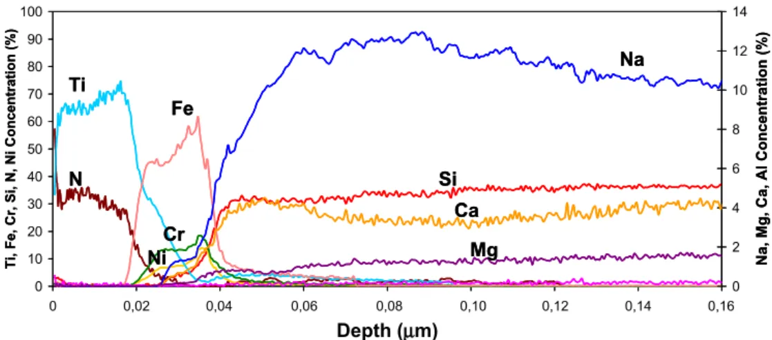
demonstrated the ability of rf-GD-OES to obtain quantitative depth profiles of ultra-thin coated glasses, as shown in Fig. 1. In this work it was observed that changes in the discharge conditions due to the thick-ness of the glass, the power applied and the presence/ absence of conductive layers on the glass did not affect the excitation conditions of the plasma [13].
In contrast to the usual relatively thick (μm) coating analysis carried out using GD, the presence of various species of gaseous elements (oxides, hydroxides, and so on) originating from adsorbed gases and passivation/ oxide layers need to be taken into account in thin film analysis. The big challenge for GD thin film analysis is to correct for all of the main interchange effects of gaseous molecules and passivation layers (with mostly unknown structures and densities) by pinpointing their effects upon glow discharge physics and spectroscopy processes [14].
On the other hand, GD-MS also provides the potential for direct solid analysis because it offers the important ad-vantages of isotopic information and lower limits of detec-tion in comparison to OES. Indeed, GD-MS is the preferred analytical technique for the certification of high purity materials such as those used in the semiconductor industry. Moreover, the different types of mass analyzer used in GD-MS has a direct influence on the analytical characteristics, applications and costs of the technique. Here, two represen-tative examples are discussed:
The coupling of a GD to a sector field mass analyzer (GD-SFMS) provides high sensitivity and high mass resolution (up to 10,000) and is currently the only GD-MS instrument available on the market (see the Finnigan ELEMENT GD for example). Moreover, there are no commercial rf-GD-MS sources, so the analysis of nonconductive materials is not directly available. Thus, further research is needed to improve the analytical capabilities of GD-MS instruments. In this regard, the influence of the design of the GD source in GD-SFMS has recently been evaluated in order to obtain adequate crater shapes for depth profile analysis of solid samples, while maintaining high sensitivity and stability [15]. Furthermore, the fact that all GD-SFMS mass analyzers
are sequential in nature is a serious limitation in depth profiling applications. Even though the ablation rates in GD-MS are∼5× slower than those in GD-OES, the user is very limited in terms of the number of elements that can be monitored effectively. In addition, the models and methods used to compute quantitative depth profiles by GD-MS are at a very primitive stage in comparison to GD-OES.
The coupling of a GD to a time of flight mass analyzer (GD-TOFMS) provides the ability to collect complete mass spectra at high repetition rates (20 kHz). More-over, the precision, sensitivity and resolution achiev-able does not depend upon the number of isotopes of interest. Due to these unique properties, GD-TOFMS offers great potential in the analysis of thin film layers, where the composition of the sample changes rapidly 0 10 20 30 40 50 60 70 80 90 100 0 0,02 0,04 0,06 0,08 0,10 0,12 0,14 0,16
Ti, Fe, Cr, Si, N, N
i C oncentration (%) 0 2 4 6 8 10 12 14
Na, Mg, Ca, Al Concentration (%)
Depth ( m) Na Si Ca Mg Fe Cr Ti N Ni
Ti, Fe, Cr, Si, N, N
i C
oncentration (%)
Na, Mg, Ca, Al Concentration (%)
µ Na Si Ca Mg Fe Cr Ti N Ni Fig. 1 Quantitative in-depth
profile of a nonconducting coated glass (substrate thickness=5.8 mm; film thicknesses=30 nm TiN/20 nm Fe-Ni-Cr/Glass) recorded by rf-GD-OES (pressure was kept at 450 Pa and forward power at 20 W)
Fig. 2 GD-OES depth-quantified profile of the multilayer coating consisting of 5 nm Cr layers embedded in a Ti matrix deposited on silicon. The dashed line follows the variation in chromium peak intensity with depth. The dotted vertical lines indicate the positions of the markers. The inset graph shows the profiles down to the first 350 nm. (From [16]; reproduced by permission of the Royal Society of Chemistry)
with time and quasi-simultaneous multianalyte deter-minations of many isotopes should be carried out at every sample depth [12]. However, the main drawback of this mass analyser is its low sensitivity, which is currently up to two orders of magnitude lower than that obtainable using GD-SFMS.
Depth resolution optimization parameters
During GD experiments, the sample (cathode) is sputtered very stably from the beginning of the analysis with Ar+ions of very low energy (<50 eV) and high current densities (in the order of 100 mA cm−2). The high current densities give rise to high sputtering rates (>1μm min−1), extending the film thickness that can be analyzed to hundreds of mi-crometers. Furthermore, the low Ar+ energies ensure that significant formation of “altered layers” during the sput-tering process is avoided, which is a very important pre-requisite for depth profiling analysis of ultra-thin films with high depth resolution. Ideally, the crater produced by the sputtering process should have a flat bottom with straight vertical walls that penetrate to the same depth across the crater. However, this shape is rarely obtained in practice, leading to increased mixing of consecutive layers in the coated material, affecting the depth resolution [2,16].
In order to demonstrate the high depth resolution that can be obtained with rf-GD-OES, Fig. 2 presents the quantitative profiles of ultra-thin (5 nm thick) chromium layers, implemented at different depths in a titanium matrix with a thickness of up to 3 μm. It is apparent that the different layers were properly resolved both near the sur-face and deeply embedded in the matrix, although the relative depth resolution increased with depth.
Since industry demands the chemical characterisation of thinner and thinner films, this GD technique shows great potential in the field of surface and coated materials analysis. GD currently offers a unique ability to perform depth profiling analysis of films over a very wide thickness range (1 nm–100 μm). State-of-the-art GD-OES systems are capable of similar depth resolutions to SIMS and AES, but in shorter analysis times and with less matrix effects. Further research is needed in the development of innovative rf/dc-GD sources for GD-MS (such as“fast flow GD”[15]) that will allow direct solid analysis with high sensitivity and high depth resolution. On the other hand, the next breakthrough in depth profile analysis could be the
development of a new GD-TOFMS instrument, combining rapid acquisition of complete mass spectra with high resolution and sensitivity. Moreover, the temporal gate resolution of this instrument in combination with a pulsed GD could be used to produce a tuneable source, leading to new applications in life science (for example, atomic, molecular and structural mass spectral data for an unknown sample could be obtained quasi-simultaneously [17]). Acknowledgements Support from Prof. Alfredo Sanz-Medel research group at University of Ouiedo (Spain) is gratefully acknowledged.
References
1. Wasa K, Kitabatake M, Adachi H (eds) (2004) Thin film materials technology-sputtering of compound materials. William Andrew Publishing/Noyes, New York
2. Hoffmann V, Dorka R, Wilken L, Hodoroaba V, Wetzig K (2003) Surf Interface Anal 35:575–582
3. Oswald S, Baunack S (2003) Thin Solid Films 425:9–19 4. Hrdlicka A, Otruba V, Novotny, Günther D, Kanicky V (2005)
Spectrochim Acta Part B 60:307–318 5. Payling R (1998) Spectroscopy 13:36–43
6. Shimizu K, Payling R, Habazaki H, Skeldon P, Thompson GE (2004) J Anal Atom Spectrom 19:692–695
7. Shimizu K, Habazaki H, Skeldon P, Thompson GE (2003) Surf Interface Anal 35:564–574
8. Payling R, Nelis T (eds) (2003) Glow discharge optical emission spectrometry: a practical guide. RSC Analytical Spectroscopy Monographs, Cambridge, UK
9. Marcus RK, Broekaert JAC (eds) (2003) Radio frequency glow discharges. Wiley, Chichester, UK
10. Jakubowski N, Bogaerts A, Hoffmann V (2003) Analytical glow discharges. In: Cullen M (ed) Atomic spectroscopy in elemental analysis, analytical chemistry series. Blackwell Publishing, Oxford, pp 91–156
11. Pisonero J, Costa JM, Pereiro R, Bordel N, Sanz-Medel A (2004) Anal Bioanal Chem 379:17–29
12. Pisonero J, Fernandez B, Pereiro R, Bordel N, Sanz-Medel A (2005) Trends Anal Chem (in press) DOI: 10.1016/j.trac.2005.04.019 13. Fernandez B, Bordel N, Pereiro R, Sanz-Medel A (2005) J Anal
Atom Spectrom 20:462–466
14. Michler J, Aeberhard M, Velten D, Winter S, Payling R, Breme J (2004) Thin Solid Films 447–448:278–283
15. Pisonero J, Feldmann I, Bordel N, Sanz-Medel A, Jakubowski N (2005) Anal Bioanal Chem 382:1965–1974
16. Galindo RE, Forniés E, Albella JM (2005) J Anal Atom Spectrom 20(10):1116–1120
17. Steiner RE, Lewis CL, Majidi V (1999) J Anal Atom Spectrom 14(9):1537–1541