Photovoltaic Technology: The Case for Thin-Film Solar Cells
A. Shah,
1P. Torres,
1* R. Tscharner,
1N. Wyrsch,
1H. Keppner
2The advantages and limitations of pho-tovoltaic solar modules for energy gene-ration are reviewed with their opegene-ration principles and physical efficiency limits. Although the main materials currently used or investigated and the associated fabrication technologies are individually described, emphasis is on silicon-based solar cells. Wafer-based crystalline sili-con solar modules dominate in terms of production, but amorphous silicon solar cells have the potential to undercut costs owing, for example, to the roll-to-roll production possibilities for modules. Recent develop-ments suggest that thin-film crystalline silicon (especially micro-crystalline silicon) is becoming a prime candidate for future photovoltaics. The photovoltaic (PV) effect was discovered in 1839 by Edmond Becquerel. For a long time it remained a scientific phenomenon with few device applications. After the intro-duction of silicon as the prime semiconductor material in the late 1950s, silicon PV diodes became available. They were soon indispens-able for supplying electrical power to tele-communications equipment in remote loca-tions and to satellites. Then, in the 1970s, a major reorientation took place in the general perception of the energy supply problem: The oil crisis of 1973 led to a general public awareness of the limitation of fossil fuels; many governments (including those of the United States, Japan, and several European
1Institute of Microtechnology (IMT), University of Neuchaˆtel, Rue A.-L. Breguet 2, CH-2000 Neuchaˆtel, Switzerland.2University of Applied Science, Avenue de l’Hoˆtel-de-Ville 7, CH-2400 Le Locle, Switzerland. *To whom correspondence should be addressed. E-mail: [email protected]
countries) started, a few years later, ambi-tious programs in the search for alternative energy sources, including PV solar energy. This trend was reinforced by public contro-versy over nuclear fission reactors and by a series of accidents in nuclear power stations, especially those of Three Mile Island (in 1979) and Chernobyl (in 1986).
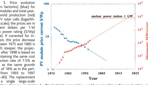
Since the beginning of the 1990s, ecolog-ical considerations linked with the CO2 /glob-al warming problem have taken over as a main driving force in promoting alternative energy sources, in particular, PV solar ener-gy. The past two decades have seen constant and substantial progress in the field of PV modules: commercial prices of modules (when purchased in large quantities) have shown a sustained average reduction of 7.5% per year; during the same time, the worldwide production of modules has increased on av-erage by 18% per year (Fig. 1). Although these two trends can be expected to continue in the near future, it will take many decades before PV modules can substantially contrib-ute to electricity generation. The reduction in PV module cost progresses with the increase of production, but we are rapidly reaching a stage where a further decrease in cost is conditional on the global availability of raw materials. Thus, PV technologies that involve the use of lesser quantities of cheaper and less refined input materials are favored.
The present cost of electricity from PV in-stallations is generally (except in remote areas) about an order of magnitude higher than the current commercial prices of electricity gener-ated by hydraulic power and nuclear and fossil fuels. Because of physical reasons, it appears at present to be very difficult to substantially in-crease the energy conversion efficiency of low-cost PV modules over 15%. Thus, it becomes necessary to reserve large surfaces for the PV generation of electricity, which also means that the costs of substrates, encapsulation, wiring, and supporting structures are decisive factors in the cost breakup of PV solar installations. This requires a full integration of PV installations into the existing environment and habitat.
Although solar cells and PV installations do not generate any CO2during their opera-tion, they do, however, consume considerable amounts of energy and cause the generation of CO2 and certain pollutants during their manufacture. The energy payback time and the ecological balance sheet of solar modules and PV installations are, therefore, important issues to be considered when choosing a fu-ture technology.
PrincipleofOperationofPVSolarCells
semiconductor diode. The semiconductor ma-terial absorbs the incoming photons and con-verts them into electron-hole pairs. In this pho-togeneration step, the decisive parameter is the bandgap energy Egap of the semiconductor. In an ideal case, no photons with an energy h ⬍ Egapwill contribute to photogeneration, where-as all photons with an energy h ⬎ Egapwill each contribute the energy Egap to the photoge-nerated electron-hole pair, with the excess en-ergy (h ⫺ Egap) being very rapidly lost be-cause of thermalization.
The maximum limit for the photogener-ated electric current density Jphis therefore given by the flux of photons with an energy h ⬎ Egap. Thus, Jphdecreases with increas-ing bandgap Egap. At the same time, the net energy transferred to each electron-hole pair increases, as it is equal to Egap. There exists an “optimum” for Egap(⬃1.1 eV) for which a maximum of energy can be transferred from the incident sunlight to the totality of photoge-nerated electron-hole pairs. At this bandgap, roughly half of the incident solar energy is transferred.
This limit will only be approached if op-tical losses due to reflections, shading by grid patterns, and so forth are minimized and if the semiconductor is thick enough to absorb all useful incident photons. The latter condition is particularly difficult to fulfill in semicon-ductors with an indirect bandgap (such as crystalline silicon), because of their low val-ues of absorption coefficients, but is more favorable in amorphous semiconductors or in semiconductors with a direct bandgap. There-fore, crystalline silicon can only be used for solar cells if it is either relatively thick (⬃100 m) or if sophisticated light-scattering (light-trapping) schemes are employed; this is one of the reasons why research into thin-film crystalline silicon solar cells has only recent-ly begun on a wide scale.
Charge separation. In the second step of the energy conversion process, the photoge-nerated electron-hole pairs are separated, with electrons drifting to one of the elec-trodes and holes drifting to the other elec-trode, because of the internal electric field created by the diode structure of the solar cell. The dark (nonilluminated) characteris-tics of the diode and the photogenerated cur-rent can, in principle, be linearly super-Photogeneration. A PV solar cell is basically a
imposed (1, 2); this results in the solar cell equivalent circuit shown in Fig. 2A and the current-voltage (I-V ) curve at the output of a solar cell, shown in Fig. 2B. Maximum pow-er can be retrieved from the solar cell at the maximum power point MPP, which is equiv-alent to the product of the open-circuit volt-age Voctimes the short-circuit current density Jsctimes the fill factor FF (FF expresses the form of the I-V curve). Jsc, Voc, and FF are the three key parameters characterizing solar cell performance. The maximum limit for Jsc is given by the photogenerated current densi-ty Jph.
Voc, on the other hand, cannot exceed Egap/q (q is the charge of an electron) and is, in general, quite a bit lower owing to recom-bination. At open-circuit conditions, all pho-togenerated carriers recombine within the so-lar cell diode. Thus, if recombination can be minimized, Voc can more closely approach the limit (Egap/q). However, from thermody-namic considerations of the balance between radiation and generation, one finds that re-combination cannot be reduced below its ra-diative component, yielding a lower basic limit for Voc(3).
Considering FF, Green (1) has calculated it as a function of Vocby assuming that the I-V characteristics of a diode are, in an ideal case, an exponential function. The calculations show that the limit for FF increases with Egap. The optimum value of Egap for the total energy conversion efficiency (including charge separation) is⬃1.5 eV, with a “limit” efficien-cy approaching 30% (4 ). Gallium arsenide (GaAs), indium phosphide (InP), and cad-mium telluride (CdTe) are semiconductor materials that have bandgap energies very near to the optimum value. However, the first two are too costly for large-scale ter-restrial applications, and CdTe has toxicity problems. With crystalline silicon, labora-tory cells have been produced that are near the corresponding efficiency “limit” of 25% (4 ). However, such record cells are based on sophisticated designs and are not suited for large-scale commercial utiliza-tion. As we go from small-size, expensive laboratory cells to large-area, low-cost commercial modules, various additional losses must be allowed for, and compro-mises between performance and cost must be found; therefore, one often ends up with module efficiencies that are, in the best case,⬃15%.
A way to increase efficiency over the above limits would be to use multijunction cells (tandems and triple junctions) by opti-cally cascading two or more solar cells with different bandgaps. This concept has led to interesting laboratory experiments, in which very high efficiencies [up to 32.6%, with sunlight concentration (5)] are demonstrated
in complicated setups that have, however, no importance for commercial modules. On the other hand, tandems and triple junctions are at present used in amorphous silicon solar cells, with the goal of reducing the effect of light-induced degradation observed there.
Finally, concentration of sunlight also re-sults in a higher theoretical efficiency limit: The balance between photogeneration and recombination described above becomes more favorable; thereby, Voc and FF are increased. The use of higher light intensities is associated, however, with serious practical problems: Higher current densities and higher tempera-tures have to be handled. Moreover, the op-tical concentrator itself and the mechanical light tracking add to the complexity and cost of the system. Thus, concentrator solar cells have not found a large field of practical application.
Figure 3 shows the evolution of record laboratory efficiencies for small-size solar cells for different technological options over the past 45 years. All thin-film technologies show an efficiency evolution curve that is similar to that of crystalline silicon, but with a delay of⬃10 years. Ribbon silicon (actu-ally a bulk crystalline silicon technology) has not achieved any substantial lead over thin-film technologies. No stabilized efficiencies can be given for dye cells, as their stability problems are not yet fully solved.
PV Technologies
Crystalline silicon solar cells: The trend to-ward thin-film crystalline silicon. As⬎80% of solar cells produced at present are crystal-line silicon solar cells (6 ) and the remaining 20% are mostly amorphous silicon solar cells (which are mainly restricted to consumer electronics), almost all PV systems with ⬎1-kW peak power rating (⬎1-kWp) are fitted with crystalline silicon solar cells. These solar cells were until very recently exclusively based on the use of silicon wafers. Alterna-tive structures, such as silicon ribbons, are just being introduced into the market.
Wafer-based crystalline silicon solar cells have relatively high efficiencies, with com-mercial modules having efficiencies between 12 and 16% and laboratory cells having a record efficiency of 24.4% (7). These cells have already proven their excellent stability and reliability, operating under outdoor con-ditions without any deterioration in their per-formance over several decades. The main disadvantage associated with this technology is, however, the resulting high module price (presently about $4.50 per 1-W peak power rating). This high price has set the amount for PV modules in general, as (until very recent-ly) cheaper modules based on other technol-ogies were simply not available. The high
production cost is a consequence of several factors: (i) the low production volume of present manufacturing plants [recent studies indicate, that about a factor of 2 could be gained in cost reduction if the production volumes were upscaled by an order of mag-nitude (8)], (ii) the complex production steps involved in cell manufacturing and in module assembly, and, especially, (iii) the large amount of highly purified silicon feedstock required (20 kg of feedstock for every 1 kWp of module production). The feedstock prob-lem limits the cost reduction potential of wafer-based silicon technology. Until 1995, the PV industry mainly used rejects from the microelectronics industry; it could, thus, ob-tain silicon feedstock at reduced prices. With the growth of the PV industry, this source of feedstock supply became insufficient. Silicon feedstock supply will remain a serious bot-tleneck until production plants for directly supplying “solar-grade silicon” are set up: These plants would then be able to supply a cheaper and less pure form of silicon than what is currently used for the microelectron-ics industry.
The fact that wafers have to be cut from an ingot with a mechanical saw creates other serious impediments for wafer-based technol-ogy: It is expensive, involves considerable material loss, and can result in the breakage of thin wafers. Furthermore, wafers are lim-ited in size and must be externally assembled and series connected to form larger modules. In this context, square-shaped “multicrystal-line” wafers cut from cast polysilicon ingots are more convenient to assemble than the circular-shaped monocrystalline wafers. Mul-ticrystalline wafers are also cheaper, but they generally result in cells and modules with conversion efficiencies that are 2 to 4% lower than those obtained with monocrystalline wa-fers. Wafer-based silicon technology has the potential to be ecologically acceptable (9), but it implies a substantial amount of fabri-cation energy, so-called “gray energy” (10).
Among all the methods investigated for the further improvement of wafer-based crystalline silicon technology, only two schemes will be mentioned here. The first scheme consists of forming the solar cell within a high-quality epitaxial layer grown on top of a silicon wafer. Although high efficiencies (⬎19%) (11–13) and high deposition rates (0.5 m/min) for epitaxial growth at temperatures of⬃500° to 600°C (14) have been demonstrated with lab-oratory methods, the transfer of these tech-niques to economically viable schemes [for ex-ample, multiple reutilization of the original sil-icon wafer or, alternatively, growth of an epi-taxial layer on top of a laser-crystallized hydrogenated amorphous silicon (a-Si:H) layer on glass] has resulted in cell efficiencies that are only⬃10 to 12% (15, 16).
The second scheme is based on the depo-sition of a doped amorphous silicon layer on the crystalline wafer to form a heterojunction (17 ). Another amorphous silicon layer can be deposited on the opposite side of the wafer (18, 19) to form the back surface field and obtain back-side passivation, increasing the efficiency to 20.0% for laboratory cells. Cor-responding pilot production of cells and mod-ules has been announced (20). The advantage of this scheme is simplified cell processing combined with a relatively high efficiency.
Crystalline silicon ribbons and crystalline silicon layers (on substrates) do away complete-ly with the need for producing wafers by saw-ing. Research on these ribbons and layers has been under way for⬃20 years and is only now entering the production phase. These cells are based on multicrystalline silicon material ob-tained directly from the liquid phase. The tem-perature of ribbon or layer formation is thus given by the melting point of silicon and is ⬃1412°C. Such a high temperature limits the choice of substrates. These ribbon-forming schemes also suffer from a problem of thermal and mechanical stress, because of the high ther-mal gradients (on the order of 500°C/cm) present near the solid-liquid interface. In addi-tion, the feedthrough rates for forming ribbons with satisfactory material quality are relatively low (around 18 mm/min) (21).
Several megawatt peak power ratings (MWp) of solar modules based on ribbons are currently being produced with the edge-film growth method (22). Laboratory efficiencies have been as high as 14%. In an alternative approach, the string ribbon method is being modified so that substrates are no longer required, and an efficiency of 15.4% has been demonstrated for laboratory cells (23); but, commercial modules are not yet available. Researchers at the Institute of Energy Con-version at the University of Delaware have developed modules based on a 50-m-thick silicon layer deposited on a ceramic substrate (24 ). They use a method for integrated mono-lithic series connection of submodules that is similar to the one developed for amorphous silicon and other thin-film modules. Efficien-cies reported recently for a 320-cm2module are 9.79% (25). It can be expected that these methods will yield some cost advantage as compared to conventional wafer-based crys-talline silicon modules, but at the price of reducing the efficiency.
stainless steel, aluminum, or sometimes even polymers. They also permit, in principle, ef-ficient grain-boundary passivation by hydro-gen incorporation into the growing crystalline layer. Thus, even at grain sizes well below 1 m, satisfactory layer properties can be ob-tained. To keep the required total thickness of the solar cell as low as possible (preferably ⬍2 m), one must employ an efficient form of light scattering or light trapping. This is achieved with surface texturing of the silicon layer as it is deposited and of the contact layers, especially of the transparent conduc-tive oxides (TCO) used in our examples. So far, the most promising results have been obtained by plasma-enhanced chemical vapor deposition (PECVD). Deposition tempera-tures as low as 220°C can be obtained with the very high frequency (VHF) plasma dep-osition method (26). Efficiencies of up to 8.5% were reached with a cell thickness of 2.7 m. With standard PECVD at 13.56 MHz and for deposition temperatures of 500° to 550°C, an aperture cell efficiency of 10.1%was obtained for a 2.0-m-thick cell (27).
These cells have low Voc values (⬃500 mV), which could possibly be increased by optimizing crystallite nucleation and growth and thereby reducing recombination. Fig-ure 4 shows a transmission electron micros-copy (TEM) photograph of a typical micro-crystalline silicon layer incorporated in such a cell, indicating the complexity of structures involved.
From an economical point of view, present deposition rates of⬃5 to 10 Å/s (28) must be increased. Combining this increase with a cell thickness reduction to ⬃1 m, deposition times of well below 1 hour would be possible.
Crystalline silicon thin-film solar cells de-posited by PECVD can be easily combined with amorphous silicon solar cells to form tandem cells (Fig. 5); the bandgaps involved (1.1 eV for crystalline silicon and⬃1.75 eV for amorphous silicon) are very close to the theoretically ideal combination. Resulting stabilized tandem cells with efficiencies of ⬃12% have been reported (27, 29, 30).
An interesting structure for multijunction crystalline silicon solar cells was proposed by the Photovoltaics Research Centre of the Uni-versity of New South Wales (31). In this structure, the individual component solar cells are electrically connected in parallel (and not in series, as in the conventional tandem and multijunction structures). Nu-merical simulations (32) indicate that the ef-ficiency potential of such a structure is ⬃15%. It is, in principle, feasible to use a large number of individual junctions within this structure. Indeed, the delicate current-matching problem of conventional series-connected multijunction cells does not apply
Amorphous silicon solar cells. Hydroge-nated amorphous silicon was introduced as a material with a potential for semiconductor devices in the mid-1970s and is the first thin-film solar cell material that has reached
Since the past few years, there has been a strongly increasing interest in thin-film crys-talline silicon solar cells with film thickness-es of ⬍10 m. Of all the methods tested for depositing crystalline silicon thin films from the gas phase, probably the most interesting are those that operate at low temperatures (typically 200° to 500°C); they allow for the use of low-cost substrates, such as glass,
here. However, fabrication costs may become substantially higher again. A large R&D pro-gram is under way in Australia (33), but few experimental results have been published.
the stage of large-scale production (⬃20 MWp/year at present). Amorphous silicon has, in the visible range of the spectrum, a higher optical absorption coefficient than crystalline silicon and, thus, can have thick-nesses much less than 1 m. In order to reduce recombination losses, a-Si:H solar cells use the p-i-n structure, consisting of a thin p-type doped layer, a central intrinsic i-type layer (which is the photovoltaically active layer), and a thin n-type doped layer. The electrical transport in the i-type layer is assisted by an electric field.
The deposition of amorphous silicon layers for solar cells is generally carried out with PECVD, which allows for deposition of large areas (up to 1 m2 or more); generally, the a-Si:H solar cell is deposited on glass coated with a TCO; the TCO layer is either SnO2or ZnO and acts as a front contact. In an alterna-tive structure, the amorphous silicon solar cell is deposited on an opaque substrate, such as stainless steel or even a polymer. The stainless steel or polymer substrates can be obtained as thin flexible foils, allowing a roll-to-roll depo-sition process (Fig. 6) (34). At present, indus-trial processes for amorphous silicon are limited by low deposition rates (⬃1 Å/s) and the re-sulting high deposition times (⬃1 hour) for a solar cell. The cost of producing high-quality TCO layers is another bottleneck, shared also by other thin-film solar cells. Thus, the price of amorphous silicon solar modules is, at present (for a given power output), only marginally lower than that of crystalline silicon solar mod-ules. There is, however, ample scope for future price reductions. Deposition rates can be in-creased fivefold with the VHF plasma method (35); TCO costs can be reduced by using ZnO instead of SnO2and by streamlining the whole TCO fabrication process (36).
The major handicap of amorphous silicon solar cells and modules is their low efficiency values. The present laboratory record for sta-bilized efficiency is 13%, obtained on a tri-ple-junction cell (37 ); actual commercial modules have stabilized efficiencies between 4 and 8%.
One of the main reasons for the limitation in stabilized efficiency is the Staebler-Wron-ski effect (SWE) (38), or light-induced deg-radation (Fig. 7), in which the efficiency decreases to a stabilized but lower value after ⬃1000 hours of illumination. Subsequent an-nealing at 100° to 250°C can restore the
One of the main reasons for the limitation in stabilized efficiency is the Staebler-Wron-ski effect (SWE) (38), or light-induced deg-radation (Fig. 7), in which the efficiency decreases to a stabilized but lower value after ⬃1000 hours of illumination. Subsequent an-nealing at 100° to 250°C can restore the original efficiency. It has become clear that the SWE is due to the creation of new defects (dangling bonds) that act as additional recom-bination centers. Despite massive research efforts, no way was found to manufacture amorphous silicon layers that do not possess such an effect. On the other hand, the SWE can be substantially reduced by diluting the silane (SiH4) source gas used for plasma-assisted deposition of amorphous silicon with hydrogen (39).
By combining thin individual cells into a tandem or a triple-junction cell, one can re-duce the detrimental effect of light-inre-duced degradation (SWE) on cell efficiency. Thin-ner layers and thinThin-ner p –i-n cells suffer less from collection problems, even if the defect density is increased by the SWE; this is be-cause, in thinner p-i-n-cells, the electric field prevailing in the i-type layer is enhanced, and collection is generally improved. Tandem and triple-junction cells also have the poten-tial for a better use of the solar spectrum, provided that the bandgap energies of the individual component cells can be adjusted accordingly. This can be partly achieved if amorphous silicon is used with amorphous alloys of silicon and germanium. The latter have lower bandgaps than amorphous silicon itself; however, they also possess higher re-combination center densities, especially for bandgaps⬍1.4 eV (40, 41). Thus, although this combination provides somewhat higher efficiencies than tandem cells with amor-phous silicon alone, there has not yet been a breakthrough here. A way out of this dilem-ma would be to combine amorphous silicon with both amorphous silicon and germanium alloys and with microcrystalline silicon; one could thus obtain bandgap energies that can be better spaced over the whole range from 1.1 eV (microcrystalline silicon) to 1.75 eV (amorphous silicon).
with an excellent ecological balance sheet; and, in the long run, the prospect of a sub-stantial cost reduction (42, 43). Only a part of these advantages are shared by other thin-film technologies.
Amorphous silicon modules appear to be the ideal future candidate for those PV appli-cations in which low cost is more important than high efficiency. They are especially suit-able for solar pumps and building integration, where a sufficient surface area can be made available without high extra cost. In the sec-tor of power supplies for small apparatuses, amorphous silicon has a dominant position and is not likely to be pushed out.
Copper indium diselenide and related ma-terials. Copper indium diselenide (CIS) and copper indium gallium diselenide (CIGS) are direct-gap polycrystalline semiconductors with very high optical absorption coefficients and are presently being widely studied for applica-tion in solar cells, with the corresponding mod-ule technology just reaching the stage of pilot production. CIS and CIGS are p-type semicon-ductors and are always used in a heterojunction
Advantages of amorphous silicon PV technology are as follows: the low deposition temperatures (typically 200° to 300°C), which permit the use of low-cost substrates; the possibility to easily integrate such mod-ules into facades, roofs, and other structures; the option of implementing monolithically integrated electrical series connections within the solar cell structure itself; the relatively low production energy and low material quantities that need to be invested in the fabrication of a module; the abundance of all raw materials involved; the potential for re-alizing a large-scale manufacturing operation
structure, mostly with very thin n-type cadmi-um sulfide (CdS) layers.
The efficiency record obtained to date for a small-size (0.449 cm2
) laboratory cell is 18.8% (44), which is impressively high for a thin-film (3m absorber thickness) polycrystalline solar cell. This is achieved with an effective bandgap of 1.1 to 1.2 eV for the absorber material: By partially substituting gallium for indium in CuInSe2, the bandgap of this semiconductor can be increased, and the PV performance is optimized by increasing Voc. A further degree of freedom is obtained by the partial substitution of S2 for Se2 (45). Other materials-oriented research efforts are directed at replacing the CdS window layer with a cadmium-free mate-rial, such as In(OH, S) (46). At present, the efficiencies of CIGS modules (30 cm by 30 cm) with integrated series connection, as fabricated in pilot production lines, are between 9 and 12% (47); this value is substantially lower than the laboratory record.
In terms of stability, CIS and CIGS solar cells do not have a problem of light-induced degradation; they generally show a slight in-crease in Vocand in efficiency during the first hours of operation and can be remarkably stable, as was proven for periods up to 8 years (48). However, they do have a problem of instability in a hot and humid environment (49).
It is expected that CIS and CIGS cells should be substantially cheaper than wafer-based crystalline silicon modules (once pro-duction can be mastered on a large scale). However, if and when CIS and CIGS solar cell technology reaches a production volume on the scale of a few 100 MWp/year, the availability and the price of indium will
be-come a major issue: The availability of in-dium in Earth’s crust is comparable to that of silver, and because of this relative scarcity, indium has been subject to erratic fluctua-tions in world market price. For example, a sharp price increase was registered around 1980, when Japanese liquid crystal display manufacturers started using large quantities of this material in their displays (4).
Cadmium telluride solar cells. Similar to CIS and CIGS, CdTe is a semiconductor with a direct bandgap, which almost fully absorbs the visible light within⬃1 m. The bandgap ener-gy, Egap⫽ 1.45 eV, is very near the optimum value for single-junction solar cells, simulta-neously yielding both high current densities Jsc (up to 26 mA/cm2) and high voltages V
oc(up to 850 mV). Because CdTe is a binary compound, CdTe solar cells and modules are easier to fabricate than those from the CIS/CIGS system. A typical CdTe solar cell structure consists of a n-CdS and p-CdTe heterojunction deposited on a glass substrate coated with a TCO. Just as in CIS/CIGS cells, the highly doped CdS layer is a very thin n-type window layer used for barrier formation and is photoelectrically inactive. The deposition of such a very thin CdS layer (to minimize the loss in blue light response) with sufficient uniformity is one of the critical issues for large-area devices. Similar to CIS/CIGS cells, most carriers are generated in the underlying p-type layer (here on the CdTe p-type layer, very close to the n-p interface), which means that, in the case of both technolo-gies, the n-p heterojunction interface is a critical region that can cause efficiency, stability problems, or both, if the deposi-tion technology is not fully mastered.
The efficiency record for CdTe solar cells is 16% on a 1-cm2laboratory cell (50). Inter-estingly, in 1992, researchers at the Univer-sity of Southern Florida reported a laboratory cell with an efficiency of 15.8% (51). It appears, therefore, that progress with the ef-ficiency of laboratory record cells is at present much less rapid in the case of CdTe technology than in the case of CIS/CIGS technology.
At present, at least two firms are building or completing large-scale manufacturing plants with a planned production capacity of 10 MWp per year (52); many others have started or an-nounced pilot production plants. Expected effi-ciencies for commercial modules are in the range of 8 to 9% for full sunlight and are somewhat lower at reduced light intensity be-cause of current losses due to grain boundaries present in these polycrystalline solar cells.
An issue that has caused a considerable amount of debate is the toxicity of cadmium (53). On one hand, CdTe is, as a compound, very stable and probably nontoxic. There are, however, definite environmental hazards and
safety issues related to the production of CdTe modules: the release of cadmium into the atmo-sphere in the case of fire, and the recycling of CdTe modules. Although these issues seem, in principle, manageable for a well-organized and politically stable industrialized country, this may not be the case for developing countries.
Thus, CdTe technology may not be a vi-able option for the future large-scale world-wide application of PV modules. The same basically applies (albeit, to a lesser extent) to CIS/CIGS solar cell technology, in its present form, because of the thin CdS layer involved. Dye-sensitized PV solar cells. An interest-ing solar cell design has been pioneered by Gra¨tzel of the Ecole polytechnique fe´d´erale de Lausanne (Switzerland) (54, 55): It is based on a rough TiO2layer covered by a light-absorbing dye and on a redox couple in a suitable electro-lyte. Charge transport is realized by the conduc-tion band of the TiO2on one side and by an ion flux within the electrolyte on the other side. This concept has the advantage of separating the tasks of carrier generation and carrier trans-port. Thus, recombination is minimized. So far, initial efficiencies of slightly more than 10% have been obtained at 100 mW/cm2light inten-sities on small (0.25-cm2) laboratory cells. The use of a liquid electrolyte, however, causes some serious additional problems: potential in-stability, limitation of maximum operation tem-perature, danger of evaporation, extra cost for forming an electrical series connection, and so forth (56, 57). These cells are, therefore, very far from the stages of commercialization and field use.
Conclusions
As the production volume of PV modules continues to increase, a stage will soon be reached at which the availability of raw ma-terials, production aspects, ecological consid-erations, and operational reliability (rather than laboratory performance) become the prime issues in selecting and promoting a given technology. It is safe to assume that thin-film solar cells will play an increasing role in the future PV market. On the other hand, any newcomer to the production scene will, for obvious reasons, have a very hard time in displacing well-established materials and technologies, such as crystalline and amorphous silicon. One should not forget that, in the cases of crystalline and amor-phous silicon, PV technology profits from the wide experience base of the microelectronics and the display industries, respectively: How-ever, no such synergy is present for CIS and CdTe. One should also look at the production risks and at the ecological balance sheet of these technologies. The case of silicon is very clear and well documented, whereas the PV
ecotoxological institutions for CIS and CdTe. Finally, because of the development of effec-tive low-cost techniques for light trapping, it is no longer absolutely necessary to use a direct-bandgap semiconductor to obtain suf-ficient optical absorption in a thin-film PV solar cell. This again supports the case for silicon as the future prime PV material.
PV technologies cater to a very wide range of different requirements. One can therefore expect, especially with future growth in production and market volume, that at least two or three different PV tech-nologies will coexist, each of them dedicated to a different sector of applications.
References and Notes
1. M. A. Green, Solar Cells: Operating Principles, Tech-nology and System Applications (Prentice-Hall, Upper Saddle River, NJ, 1982).
2. H.-G. Wagemann and H. Eschrich, Grundlagen der photovoltaischen Energieumwandlung (B. G. Teubner, Stuttgart, Germany, 1994).
3. H. Kiess and W. Rehwald, Sol. Energy Mater. Sol. Cells
38, 45 (1995).
4. A. Shah, R. Platz, H. Keppner, ibid., p. 501. 5. M. A. Green, K. Emery, K. Bu¨cher, D. L. King, S. Igari,
Prog. PV Res. Appl. 6, 35 (1998).
6. G. Giroult-Matlakowski, U. Theden, A. W. Blakers, in Proceedings of the 2nd World Conference on PV Solar Energy Conversion, J. Schmid et al., Eds. (European Commission, Directorate General Joint Research Cen-ter, Ispra, Italy, 1998), pp. 3403–3406.
7. J. Zhao, A. Wang, M. A. Green, F. Ferrazza, Appl. Phys. Lett. 73, 1991 (1998).
8. C. E. Witt et al., in Proceedings of the 1st IEEE World Conference on PV Energy Conversion (Institute of Electrical and Electronics Engineers, Piscataway, NJ, 1994), pp. 2262–2270.
9. Y. S. Tsuo et al., in Proceedings of the 2nd World Conference on PV Solar Energy Conversion, J. Schmid et al., Eds. (European Commission, Directorate Gen-eral Joint Research Center, Ispra, Italy, 1998), pp. 1199–1204.
10. G. Hagedorn, Kumulierter Energieaufwand von Pho-tovoltaik und Windkraftanlagen (Technischer Verlag Resch KG, Mu¨nich, 1992).
11. R. Brendel, M. Hirsch, R. Plieninger, J. H. Werner, in Proceedings of the 13th European Commission Pho-tovoltaic Solar Energy Conference, W. Freiesleben et al., Eds. (H. S. Stephens, Bedford, UK, 1995), pp. 432–435.
12. J. Zhao, A. Wang, S. R. Wenham, M. A. Green, ibid., pp. 1566–1569.
13. C. Hebling, S. Reber, K. Schmidt, R. Lu¨demann, F. Lutz, in Proceedings of the 26th IEEE Photovoltaic Special-ists Conference (Institute of Electrical and Electronics Engineers, Piscataway, NJ, 1997), pp. 623–626. 14. R. B. Bergmann, C. Zaczek, N. Jensen, S. Oelting, J. H.
Werner, Appl. Phys. Lett. 72, 2996 (1998). 15. R. B. Bergmann et al., paper presented at the 5th
International Conference on Solar Energy Storage and Applied Phototchemistry SOLAR 99, Cairo, 3 March to 4 April 1999. Abstract available at: www.uni-stuttgart.de/ipe/papers/publ_99/bergm99_thin.htm 16. H. Tayanaka, K. Yamauchi, T. Matsushita, in
Proceed-ings of the 2nd World Conference on PV Solar Energy Conversion, J. Schmid et al., Eds. (European Commis-sion, Directorate General Joint Research Center, Ispra, Italy, 1998), pp. 1272–1277.
17. T. Takahama et al., in Proceedings of the 11th Euro-pean Commission Photovoltaic Solar Energy Confer-ence, L. Guimaraes et al., Eds. (Harwood Academic, Chur, Switzerland, 1992), pp. 1057–1060. 18. P. Torres, H. Keppner, R. Flu¨ckiger, J. Meier, A. Shah, in
Proceedings of the 12th European Commission Pho-tovoltaic Solar Energy Conference, R. Hill, W. Palz, P. Helm, Eds. (H. S. Stephens, Bedford, UK, 1994), pp. 132–135.
19. T. Sawada et al., in Proceedings of the 1st IEEE World Conference on PV Energy Conversion (Institute of Electrical and Electronics Engineers, Piscataway, NJ, 1994), pp. 1219–1226.
20. Double-sided solar modules have been developed by Sanyo Solar Industries (www.sanyo.co.jp/index_e. html).
21. R. L. Wallace, R. E. Janoch, J. I. Hanoka, in Proceedings of the 2nd World Conference on PV Solar Energy Conversion, J. Schmid et al., Eds. (European Commis-sion, Directorate General Joint Research Center, Ispra, Italy, 1998), pp. 1818–1821.
22. R. L. Wallace, J. I. Hanoka, S. Narashima, S. Kamra, A. Rohatgi, in Proceedings of the 26th IEEE Photovoltaic Specialists Conference (Institute of Electrical and Electronics Engineers, Piscataway, NJ, 1997), pp. 99– 102.
23. J. P. Kalejs and W. Schmidt, in Proceedings of the 2nd World Conference on PV Solar Energy Conversion, J. Schmid et al., Eds. (European Commission, Director-ate General Joint Research Center, Ispra, Italy, 1998), pp. 1822–1825.
24. A. M. Barnett et al., in Proceedings of the 8th European Commission Photovoltaic Solar Energy Conference, I. Solomon, B. Equer, P. Helm, Eds. (Kluwer Academic, Dordrecht, Netherlands, 1988), pp. 149–155. 25. D. H. Ford et al., in Proceedings of the 2nd World
Conference on PV Solar Energy Conversion, J. Schmid et al., Eds. (European Commission, Directorate Gen-eral Joint Research Center, Ispra, Italy, 1998), pp. 1205–1208.
26. J. Meier et al., Mater. Res. Soc. Symp. Proc. 507, 139 (1998).
27. K. Yamamoto et al., ibid., p. 131.
28. P. Torres et al., in Proceedings of the 26th IEEE Photovoltaic Specialists Conference (Institute of Elec-trical and Electronics Engineers, Piscataway, NJ, 1997), pp. 711–714.
29. J. Meier et al., J. Non-Cryst. Solids 227–230, 1250 (1998).
30. K. Saito et al., in Proceedings of the 2nd World Conference on PV Solar Energy Conversion, J. Schmid et al., Eds. (European Commission, Directorate Gen-eral Joint Research Center, Ispra, Italy, 1998), pp. 351–354.
31. M. A. Green and S. R. Wenham, Appl. Phys. Lett. 65, 2907 (1994).
32. S. R. Wenham et al., in Proceedings of the 1st IEEE World Conference on PV Energy Conversion (Institute of Electrical and Electronics Engineers, Piscataway, NJ, 1994), pp. 1234–1241.
33. Annual Review (Pacific Solar Pty., Sydney, Australia, 1998).
34. H. Morimoto and M. Izu, in Amorphous Semiconduc-tor Technologies and Devices, vol. 16 of Japan Annual Review in Electronics, Computers, and Telecommuni-cations, Y. Hamakawa, Ed. (North-Holland, Amster-dam, 1984), pp. 212–221.
35. H. Curtins, N. Wyrsch, M. Favre, A. Shah, Plasma Chem. Plasma Process. 7, 267 (1987).
36. A. Lo¨ffl et al., in Proceedings of the 14th European Commission Photovoltaic Solar Energy Conference, H. A. Ossenbrink, P. Helm, H. Ehmann, Eds. (H. S. Stephens, Bedford, UK, 1997), pp. 2089–2092. 37. J. Yang, A. Banerjee, S. Guha, Appl. Phys. Lett. 70,
2975 (1997).
38. D. L. Staebler and C. R. Wronski, ibid. 31, 292 (1977). 39. S. Guha, K. L. Narasimhan, S. M. Pietruszko, J. Appl.
Phys. 52, 859 (1981).
40. J. Fo¨lsch et al., Mater. Res. Soc. Symp. Proc. 377, 517 (1995).
41. S. Guha, in Proceedings of the 25th IEEE Photovoltaic Specialists Conference (Institute of Electrical and
community does not have access to the inde-pendent and in-depth studies of specialized
Electronics Engineers, Piscataway, NJ, 1996), pp. 1017–1022.
42. P. R. Wolfe and S. W. Jansen, in Proceedings of the 2nd World Conference on PV Solar Energy Conversion, J. Schmid et al., Eds. (European Commission, Direc-torate General Joint Research Center, Ispra, Italy, 1998), pp. 1901–1905.
43. R. Crandall and W. Luft, Prog. PV Res. Appl. 3, 315 (1995).
45. T. M. Friedelmeier and H. W. Schock, in Proceedings of the 2nd World Conference on PV Solar Energy Conversion, J. Schmid et al., Eds. (European Commis-sion, Directorate General Joint Research Center, Ispra, Italy, 1998), pp. 1117–1120.
46. B. M. Basol, U. K. Kapur, C. R. Leidholm, A. Minneck, A. Halami, in AIP Conference Proceeding No. 306, R. Nofi and H. Ullal, Eds. (American Institute of Physics, New York, 1994), pp. 79–82.
47. B. Dimmler et al., in Proceedings of the 2nd World Conference on PV Solar Energy Conversion, J. Schmid et al., Eds. (European Commission, Directorate Gen-eral Joint Research Center, Ispra, Italy, 1998), pp. 419–423.
48. H. S. Ullal, K. Zweibel, B. vonRoedern, in Proceedings of the 26th IEEE Photovoltaic Specialists Conference (Institute of Electrical and Electronics Engineers, Pis-cataway, NJ, 1997), pp. 1161–1163.
49. J. Wennerberg, J. Kessler, M. Bodegard, L. Stolt, in Proceedings of the 2nd World Conference on PV Solar Energy Conversion, J. Schmid et al., Eds. (European Commission, Directorate General Joint Research Cen-ter, Ispra, Italy, 1998), pp. 1161–1164.
50. H. Ohyama et al., in Proceedings of the 26th IEEE Photovoltaic Specialists Conference (Institute of Elec-trical and Electronics Engineers, Piscataway, NJ, 1997), pp. 343–346.
51. T. L. Chu et al., in Proceedings of the 11th European Commission Photovoltaic Solar Energy Conference, L. Guimaraes et al., Eds. (Harwood Academic, Chur, Switzerland, 1992), pp. 988–990.
52. W. Fuhs and R. Klenk, in Proceedings of the 2nd World Conference on PV Solar Energy Conversion, J. Schmid et al., Eds. (European Commission, Directorate Gen-eral Joint Research Center, Ispra, Italy, 1998), pp. 381–385.
53. V. M. Fthenakis and P. D. Moskowitz, Prog. PV Res. Appl. 3, 295 (1995).
54. B. O’Regan and M. Gra¨tzel, Nature 353, 737 (1991). 55. M. K. Nazeeruddin et al., J. Am. Chem. Soc. 115, 6382
(1993).
56. J. M. K. E. Rijnberg et al., in Proceedings of the 2nd World Conference on PV Solar Energy Conversion, J. Schmid et al., Eds. (European Commission, Director-ate General Joint Research Center, Ispra, Italy, 1998), pp. 47–52.
57. G. Chmiel, J. Gehring, I. Uhlendorf, D. Jestel, ibid., p. 53–57.
58. Report PVPS 1-06 (International Energy Agency, Paris, 1998).
59. A. Riccaud, in Proceedings of the 12th European Com-mission Photovoltaic Solar Energy Conference, R. Hill, W. Palz, P. Helm, Eds. (H. S. Stephens, Bedford, UK, 1994), pp. 7–14.
60. For shipment volumes, see Photovoltaic Insider’s Re-port (available at www.pvinsider.com/).
61. J. Merten, J. M. Asensi, A. Shah, J. Andreu, in Proceed-ings of the 14th European Commission Photovoltaic Solar Energy Conference, H. A. Ossenbrink, P. Helm, H. Ehmann, Eds. (H. S. Stephens, Bedford, UK, 1997), pp. 260–263.
62. M. Camani, N. Cereghetti, D. Chianese, S. Rezzonico, ibid., pp. 709–712.
63. The contributions of many members of the thin-film silicon research group at IMT are gratefully acknowl-edged, in particular, those of J. Meier, Y. Ziegler, U. Kroll, D. Fischer, and S. Baillod. Special thanks are due to the contributions of K.-D. Ufert (Siemens Solar GmbH) and S. Nowak (program coordinator of Swiss R&D program in PV).
Fig. 1. Price evolution
(from factories) (blue) for PV modules and total year-ly world production (red) of PV solar cells (logarith-mic scale); the prices are in current dollars per 1-W peak power rating ($/Wp) (blue). If corrected for in-flation, the price decrease between 1975 and 1985 is much steeper; the projec-tion after 1998 is based on maintaining the same cost reduction rate of 7.5% as well as the same growth rate of 18% as in the peri-od from 1993 to 1997 (58–60). The replacement of a single large-scale
1-GW nuclear power station by PV electricity generation would require (depending on location and climate) between 5000 MWpand 10,000 MWpof PV modules.
Fig. 2. (A) Electrical equivalent circuit of a PV
solar cell (61). The diode is a dark (nonillumi-nated) p-n or p–i-n diode. Additional recombina-tion (particularly in the i-type layer of p–i-n di-odes) is represented by the current source, which counteracts the photogenerated current. Rsand Rshare resistors that represent electrical losses (for example, Rslosses due to contact resistance and Rshlosses due to pinholes through the solar cell). (B) Typical I-V characteristics of a solar cell, with the three characteristic parameters: short-circuit current Isc, open-circuit voltage Voc, and fill factor FF⫽ Pmax/(Voc⫻ Isc); Pmaxis the electrical power delivered by the cell at the maximum power point MPP.
Fig. 3. Record efficiency
evolution of small-size lab-oratory solar cells of vari-ous technologies [see (5) and references cited in (5)].
Fig. 4. TEM cross-section micrograph of typical
intrinsic microcrystalline silicon layer as depos-ited by PECVD and used for p–i-n solar cells (26).
Fig. 5. Microcrystalline and amorphous silicon
tandem solar cell, as introduced by the IMT (so-called “micromorph” solar cell) (26) Scale bar, 2m.
Fig. 6. Principle of
roll-to-roll deposition pro-cess for the deposition of amorphous silicon solar cells on flexible substrates (here, stain-less steel) (34). The PECVD process is usu-ally operated at the ra-dio frequency (RF) of 13.56 MHz.
Fig. 7. Typical efficiency
performance of amor-phous silicon modules as measured at the TISO outdoor testing site near Lugano (Switzerland). Because of the SWE, the efficiency first decreases but recovers periodically (at least partly) during the warmer summer months; during a period of⬎10 years, the ampli-tude of these seasonal variations steadily de-creases with efficiencies tending toward the low-er value of the wintlow-er months (62). Blue