HAL Id: tel-01346834
https://hal.archives-ouvertes.fr/tel-01346834v2
Submitted on 23 Jul 2016HAL is a multi-disciplinary open access archive for the deposit and dissemination of sci-entific research documents, whether they are pub-lished or not. The documents may come from teaching and research institutions in France or abroad, or from public or private research centers.
L’archive ouverte pluridisciplinaire HAL, est destinée au dépôt et à la diffusion de documents scientifiques de niveau recherche, publiés ou non, émanant des établissements d’enseignement et de recherche français ou étrangers, des laboratoires publics ou privés.
Cathodoluminescence in semiconductor structures under
local tunneling electron injection
Petr Polovodov
To cite this version:
Petr Polovodov. Cathodoluminescence in semiconductor structures under local tunneling electron injection. Optics [physics.optics]. Ecole Doctorale de l’Ecole Polytechnique, 2015. English. �tel-01346834v2�
Thèse présentée pour obtenir le grade de
DOCTEUR DE L'ÉCOLE POLYTECHNIQUE
Spécialité : Physique Par
Petr POLOVODOV
Cathodoluminescence in semiconductor structures
under local tunneling electron injection
Soutenue le 21 décembre 2015 devant le jury composé de :
M. Fabrice Charra CEA/Saclay, Gif sur Yvette Rapporteur
M. Philippe Dumas CINaM, Marseille Rapporteur
M. Razvigor Ossikovski LPICM, Ecole Polytechnique, Palaiseau Examinateur
M. Oleg Tereshchenko Rzhanov Institute of Semiconductor Physics, Novosibirsk, Russie
Examinateur
M. Yves Lassailly LPMC, Ecole Polytechnique, Palaiseau Directeur de thèse
3
ACNOWLEGEMENTS
I have defended my PhD thesis in physics. This is the accomplishment of myself but several persons have contributed to this work.
First of all, I am grateful to François Ozanam and Mathis Plapp, successive Directors of the Laboratory, who allowed me to perform my PhD work at the LPMC in the best possible conditions.
Then and foremost, I would like to express my gratitude to my scientific advisors, Jacques Peretti and Yves Lassailly. From the beginning there was the plethora of modifications to the STM experimental setup. Starting from the mundane STM cryostat configuration we could perform the optical detection of the transmitted current measurements. It took a lot of effort to modify the microscope. I would like to thank you, Yves with the help of the system realization. Also, the explanation of the monochromator functionality and explaining the LabVIEW programs used for the wavelength scan. Jacques, I am grateful for the discussion of the physics of GaN material and LED. Jacques and Yves, I am grateful for the presentation preparation, numerous simplifications. Thank you for your great help and availability during the experimental part of the work, as well as duri ng the drafting and defense preparation. Also, thank you for your commentaries and advices that helped me to work in more efficient way. Furthermore, I truly appreciate your patience as I worked on trying to get my thoughts written down.
Besides my advisors, I would like to express my gratitude to the members of the thesis committee: Fabrice Charra, Philippe Dumas, Razvigor Ossikovski, Oleg Tereshchenko and Fouad Maroun for agreeing to participate in the jury, as well as for the insightful and interesting discussions.
My sincere thanks also go to Daniel Paget, who provided me an opportunity to join the team as intern, and who gave access to the laboratory and research facilities. Thank you Lucio Martinelli, you have taught me STM microscopy, proposed and realized numerous solutions for the cathodoluminescence and transmission experiments. Let me also note your humor, that made difference. In regards to the mechanical devices and electronic circuits, I thank André Wack and Didier Lenoir. Fouad Maroun, thank you for the discussions concerning STM, also the LabVIEW program that has been hitherto used for the optical detection. Many thanks to Marco Piccardo for the GaN samples provided by colleagues at UCSB, and for insightful discussions. I am also indebted to Oleg Tereshchenko who provided me with advices on the life in France, with comments on the thesis presentation and with the GaAs samples that were used in the first part of my work. I would also like to thank the intern student Alex Sarracino for the help with the experiments and the sample preparation. I did appreciate to work with you. George Lampel helped me with the photomultiplier and the corresponding electronic circuits and was often available for scientific discussions; you
4
also have recommended me good physics books which were pleasure to read. Viatcheslav Safarov provided me with very clear and interesting explanations of physical phenomena. Mélanie helped me with the SEM measurements which provided fruitful information on the surface composition of my GaN samples. Thank you Viacheslav Kubytskyi and Alain Louis-Joseph for help and advices with Matlab. Catherine Henry de Villeneuve and Isabelle Maurin for the help with sample surface treatment issues. Thank you Nan Di for preparing the Au/Si samples, Florian, for teaching me how to prepare tungsten wires and tips, that were used in the early experiments. Julien Monguillon and Denis Coupvent-Desgraviers were of great help with computers. I am also grateful to Philippe Allongue for the information on electrochemistry and to Robert Cortes for your encouragement during the manuscript preparation. Anne-Marie Dujardin provided me with much help for all the administrative work and for accommodation in France.
I thank my fellow labmates in for the stimulating discussions, and for all the fun we have had in the last four years.For phd students: Lucie Devys, Nicolas Desbeufs, Maxime Ardré, Lili Lu, Nan Di, Timothy Aschl, Tapajyoti Das Gupta, Suprio Ghosh, post-docs Godefroy Leménager, María Castellano Sanz, Manon Lafouresse, Nikoletta Jegenyés for leisure. Thank you for organization of seminars, pots, parties together. Also, I am grateful for french language skills. My friends Satenik Mkhitaryan, Christophe Desages and Ekaterina Mityurova for your inspiration and help. I also wish a good defense to Satenik Mkhitaryan and Ekaterina Mityurova, Timothy Aschl, Marine Brunet, Maud Thiriet and all the PhD students.
From the personal point of view, I would like to acknowledge the great contribution of my mother for your inspiration and support. There are not enough words to express how deeply I am grateful to you.
6
RESUME
L’objectif de ce travail de thèse est d’étudier les phénomènes de transport électronique et de recombinaison à l’échelle nanométrique dans des structures semi-conductrices à puits quantiques. L’approche expérimentale retenue consiste à injecter les porteurs localement par la pointe d’un microscope à effet tunnel et à détecter la luminescence due à la recombinaison des électrons transmis à travers la structure et capturés par les puits quantiques insérés à distance de la surface. Cette mesure tout optique permet de s’affranchir des problèmes liés à la mesure électrique de très faibles courants transmis, d’envisager l’étude du transport à travers des nanostructures isolées et de réaliser une cartographie du transport aux échelles ultimes éventuellement dans des structures contactées en condition de fonctionnement. Les principaux résultats obtenus au cours de ce travail concernent l’étude de structure GaN/InGaN/GaN qui constituent la base des dispositifs électroluminescents pour l’éclairage. La spectroscopie d’excitation de la cathodoluminescence, obtenue en mesurant la lumière émise par les puits d’InGaN en fonction de l’énergie d’injection des électrons, montre deux régimes que l’on peut relier à la structure de la bande de conduction. Les images de cathodoluminescence mettent en évidence des effets de localisation des porteurs sur la recombinaison radiative dans les puits quantiques d’InGaN. Ces effets de localisation peuvent être reliés au désordre de composition de l’alliage ternaire. Par ailleurs, les conditions de forte injection nécessaires pour étudier le transport dans les structures semi-conductrices de type p de grande bande interdite produisent des modifications importantes de la surface. L’exploitation de ces phénomènes nous a permis de montrer la possibilité de modifier la surface du GaN sous la pointe tunnel et de réaliser des structures artificielles de dimensions nanométriques.
8
ABSTRACT
The thesis objective is to study transport and recombination phenomena at the nanoscale in semiconductor structures incorporating quantum wells. The experimental approach consists in injecting electrons locally by the tip of a scanning tunneling microscope and detecting the luminescence due to the recombination of electrons transmitted through the structure and captured by the quantum wells inserted at a distance from the surface. This all-optical measurement overcomes some of the limitations associated with usual techniques based on the electrical measurement of very small transmitted currents. In particular, it should allow addressing hot-electron transport through isolated nanostructures or through non-rectifying heterostructures, mapping electronic transport down to ultimate scales eventually in contacted devices under operation, exploiting spin filtering effects in ferromagnetic metal/semiconductor junctions. The main results obtained in the present work concerns the study GaN / InGaN / GaN structures that form the basis of wide-bandgap light-emitting devices for lighting. Excitation spectroscopy of the cathodoluminescence, obtained by measuring the light emitted from the InGaN quantum wells as a function of the electron injection energy, shows two regimes which may be related to the conduction band structure. Imaging of the cathodoluminescence evidences localization effects on the transport and radiative recombination process. These localization effects can be due to the disorder in the InGaN ternary alloy composition. Moreover, the severe tunneling injection conditions required to investigate minority carrier transport in large bandgap p-type semiconductor structures produce significant changes in the surface composition and morphology. The exploitation of these phenomena allowed us to control the formation of tip-induced patterns of nanometric dimensions on the GaN surface.
10
CONTENT
INTRODUCTION ...12
PART 1. OPTICAL DETECTION OF BALLISTIC ELECTRON TRANSPORT IN METAL/SEMICONDUCTOR JUNCTIONS ...16
1.1 CONTEXT AND OBJECTIVES ... 18
1.1.1 Ballistic electron emission microscopy (BEEM) ... 18
1.1.2 BEEM of ferromagnetic metal/semiconductor junctions... 19
1.1.3 Optical detection of spin-dependent transport in FM/semiconductor structures ... 21
1.1.4 Our objective... 22
1.2 EXPERIMENT ... 24
1.2.1 Proposed approach ... 24
1.2.2 STM setup ... 24
1.2.3 Implementation of BEEM ... 26
1.2.4 Luminescence detection setup... 27
1.3 RESULTS ... 30
1.3.1 BEEM of Au/n-Si junctions ... 30
1.3.2 Optical detection of BEEM in Pd/Fe/GaAs/InGaAs/GaAs structures ... 35
1.3.3 Luminescence of GaAs/InGaAs/GaAs QW's structures... 37
1.4 CONCLUSION ... 46
PART 2. LOCALIZATION EFFECTS ON THE CARRIER TRANSPORT AND RECOMBINATION IN GAN/INGAN/GAN STRUCTURES ...48
2.1 CONTEXT... 50
2.1.1 Motivation ... 50
2.1.2 State of the art... 51
2.2 EXPERIMENTAL SETUP ... 54
2.2.1 Sample holder ... 54
2.2.2 Optical detection set-up: test measurements ... 55
2.3 RESULTS ... 58
2.3.1 STL spectroscopy and microscopy of InGaN/GaN structures ... 58
2.3.2 STL spectroscopy of InGaN/GaN LEDs... 66
2.3.3 STL microscopy in InGaN/GaN structures: localization effects ... 71
2.3.4 Tip-induced surface modification – nano patterning... 74
2.4 CONCLUSION ... 84
CONCLUSION AND PERSPECTIVES ...88
12
Introduction
The invention of scanning tunneling microscopy (STM) in the early 1980’s [Binnig1982], awarded by the Noble Prize in 1986 has open the way to the development of local probe microscopies which are nowadays essential tools in nanoscience. Visu alizing atoms on a solid surface [Binnig1983] still remains an amazing achievement. Beyond the exploit of imaging with atomic resolution, STM has provided a direct spectroscopic access to the electronic properties of the surface of conductors at ultimate scales. Furthermore, the local electron injection with a controlled energy below the vacuum level rapidly appeared as a powerful tool for the study of electron transport in a conduction band region hardly accessible by usual microscopy and spectroscopy techniques. With the basic two-terminal (tip and surface) STM configuration, the transport properties of the tunneling barrier are probed, limiting the technique to the study of atomic or molecular layers. With heterostructures that introduce a second barrier at a buried interface, a three-terminal configuration can however be achieved. In such a structure, that can be seen as a transistor -like device, emitter/base (tip/surface tunneling barrier) and base-collector (heterostructure) junctions are independently controlled and the measurement of the collector current as a function of the injection conditions gives access to the transport through the base and base -collector junction. This approach led to the development of ballistic electron emission microscopy (BEEM) [Kaiser1988] which allowed direct mapping of hot-carrier transport through metal/semiconductor junctions, providing measurement of Schottky barrier height and of hot-electron scattering in metallic thin films. In particular, in ferromagnetic metal/semiconductor junctions, strong spin valve effects on the ballistic transmission of electrons were demonstrated allowing high resolution magnetic domain imaging of buried ferromagnetic layers [Rippard1999, Kaidatzis2008]. However, the three-terminal approach suffers from several limitations. First, the detection of small collector currents requires a highly rectifying base-collector contact which is not obvious to achieve with any metal/semiconductor junction. Second, transport through isolated single nanostructures cannot be detected. Third, in the case of ferromagnetic metal/semiconductor junctions containing a single magnetic layer, spin-dependent transport effects can only be evidenced when using a magnetic tip, with the supplementary requirements that the tip and layer magnetizations are not orthogonal and that their directions could be independently controlled by applying an external magnetic field.
The aim of this thesis is to develop an experimental approach for studying transport and recombination phenomena at the nanoscale in semiconductor structures, based on the luminescence detection under local injection of electrons by a STM tip. In this approach, we will consider structures and devices where quantum wells (QWs) are incorporated at a certain depth from the surface of a p-type semiconductor terminal. The light emitted from the QWs will originate from the recombination of electrons injected at the sample surface,
13
transmitted through the structure and captured by the QWs. Luminescence analysis should thus provide information on the transport through the structure without the need of a three-terminal configuration. This all-optical detection technique is expected to overcome some of the previously evoked limitations associated with the electrical measurements. It should indeed allow the study of electron transport through isolated nanostructures and through heterostructures that do not exhibit a rectifying character. Note also that even the three-terminal configuration may benefit from an optical detection. For instance, it should indeed be in some cases possible to modify the potential landscape in a device (by applying bias between the three terminals) without the minority carrier (optical) detection being limited by the majority carrier current. Finally, sensitivity to spin-dependent effect should also be provided through the measurement of the luminescence polarization which is coupled to the electron spin polarization via the spin-orbit interaction [Lampel1968, Parsons1969]. With such a spin-selective optical detection, a bilayer spin-valve structure is no more necessary and spin filtering effects could in principle be measured in a single magnetic layer without the need of a magnetic tip as a source of a spin-polarized electrons.
For developing this approach, we have built an experimental setup based on a commercial Omicron STM. This instrument is designed for low temperature operation in a cryostat equipped with windows providing an optical access to the sample. We have modified the setup, on the one hand, to allow the study of contacted two-terminal devices and, on the other hand, to implement an optical spectroscopy setup capable of measuring the light emitted from the sample under tunneling electron injection by the STM tip. Setting up this experiment, we were targeting two main objectives: studying spin-filtering effects at the nanoscale in ferromagnetic metal/semiconductor junctions and evidencing localization effects in the transport and recombination in InGaN/GaN structures. The manuscript is accordingly divided in two parts.
Part 1, dedicated to the optical detection of ballistic electron transport through
ferromagnetic metal/semiconductor junctions, is organized in three chapters.
Chapter 1.1 describes the context and motivation of this study. We briefly introduce
STM and BEEM techniques and we discuss milestone results reported in the literature on the measurement of spin-dependent electron transport in ferromagnetic metal / semiconductor structures. We, in particular, discuss results obtained in this field by using an optical detection method.
In Chapter 1.2, we detail the experimental setup that we have developed and present the calibration experiments. Conventional measurements of ballistic electron transport in Au/Si-n test samples are demonstrated.
In Chapter 1.3, the study of ferromagnetic metal/semiconductor structures incorporating QWs is presented. In such structures, spin filtering effects are optimum for metallic layers of a few nanometer thickness and for low energy electrons. One of the best
14
compromise for the semiconductor collector is p-type GaAs incorporating InGaAs QWs. In Pd/Fe/GaAs/InGaAs/GaAs structures spin filtering effects have already been detected by cathodoluminescence spectroscopy in the keV electron injection energy range [Li2011]. However, the recombination light emitted from such a structure is in a near-infrared region where photon counting devices are not highly efficient. This has limited our investigations and we were not able to detect a STM-induced cathodoluminescence signal originating from the electron recombination in the InGaAs QWs.
Part 2, of the manuscript, dedicated to the study, by scanning tunneling
luminescence (STL) microscopy, of localization effects on the transport and recombination in InGaN/GaN structures, is also organized in three chapters.
In Chapter 2.1, we introduce the main issues in the physics of nitride semiconductors related to their applications in optoelectronics. In particular, we emphasize the major role of disorder-induced localization effects on the carrier density and recombination processes. This issue was already previously addressed by STL-based approaches [Evoy1998, Evoy1999a, Evoy1999b, Kemerink1999, Kemerink2001, Manson-Smith2001]. The main results are discussed.
In Chapter 2.2, are described the modifications brought to the experimental setup and procedures for the study of III-N structures. With this system, significant improvements were achieved. First, the operation spectral region shifts to the visible range around 450 nm where high EQE photomultipliers are available. Second, the implementation of a fibered light collection system allowed improving both the collection efficiency and the stability of the system. Third, more reliable calibration and alignment procedures have been implemented based on the electroluminescence of InGaN/GaN LEDs instead of photoluminescence.
In Chapter 2.3, the results obtained by STL spectroscopy and microscopy on GaN / InGaN / GaN structures are presented. These structures incorporate an InGaN QW and constitute the basis of III-N optoelectronic devices such as light-emitting diodes (LEDs) and solar cells. The STL spectroscopy shows that efficient electron capture and radiative recombination occurs in the InGaN QW. No significant luminescence signal is detected at the GaN bandgap. The STL excitation spectroscopy shows a 3.2 eV onset threshold. In order to reach the QW located beyond the band bending region, electrons have indeed to be injected above the conduction band minimum in the bulk p-GaN. The onset value of 3.2 eV indeed corresponds to the energy difference between the Г valley in the bulk p-GaN and the Fermi level. A sudden saturation of the luminescence signal is observed when electron injection energy exceeds by more than 1 eV the minimum of the conduction in the bulk. This effect is possibly due to electron injection in upper conduction valleys and consequent decrease in the carrier collection efficiency by the QW. The corresponding STL plateau provides stable conditions for STL imaging. STL microscopy measurements evidence light emission localization in a scale range between 10 to 100 nm. This emission localization is not related
15
to defects (related to dislocations) observed on the surface topography and is likely to be related to composition disorder in the QW ternary alloy. All these results have however been obtained in a severe carrier injection regime. It is shown that in these high electron injection conditions, significant modifications of the GaN surface are produced which are detrimental to STL. The crossed-characterization measurements by SEM, EDX, AFM and STM conclude to the formation of Ga oxide under the tip. Exploiting these phenomena, we demonstrate the possibility to control with the STM tip the formation of patterns of nanometric dimensions on the GaN surface.
16
Part 1. Optical detection of ballistic electron transport
in metal/semiconductor junctions
18
1.1 Context and objectives
1.1.1 Ballistic electron emission microscopy (BEEM)
Compared to STM, BEEM is a three terminal configuration (Figure 1a) which was developed for studying hot-electron transport in metal/semiconductor junctions [Kaiser1988]. Hot electrons are injected by a STM tip in the thin metal film and the electrons transmitted ballistically through the metallic layer are collected in the semiconductor substrate. The electron injection energy above the metal Fermi level is controlled by the bias Vg applied between the tip and the metal surface (Figure 1b). Most of the injected electrons relax their energy and momentum into the metal layer and cannot overcome the Schottky barrier at the metal/semiconductor interface. They are collected at the metal contact and form the current It. The Schottky barrier thus provides a high energy pass filter for ballistic electrons which can be transmitted into the semiconductor providing their injection energy is larger than the Schottky barrier height B. These electrons are collected on the semiconductor contact and form the collector current labeled Ic. The onset of Ic is expected when eVc is larger than B. Typically, Ic and It are of the order of nA and pA respectively. The ratio Ic/It characterizes the electron transmission through the metal layer and the Schottky barrier. It thus gives access to electron scattering processes in the metallic thin film and to the local potential barrier at the buried metal/semiconductor interface with typical lateral resolution of 1 nm [Bell1988]. The acceptance angle of collected electrons into the semiconductor determines the lateral resolution.
Figure 1 : (a) Principle of BEEM and (b) schematics of the corresponding energy band diagram showing electron injection and transmission into a Schottky junction. Vg is the tip-sample bias voltage. Using two contacts on the tip-sample, one on the metallic layer and one on the semiconductor substrate, hot and thermalized electron currents, Ic and It respectively, are measured separately.
The theoretical description of the BEEM current relies on free electron models based on a four-step electron transport scheme in the metal/semiconductor junction: tunneling at
19
the tip/vacuum/metal barrier, propagation of free electrons into the metal layer, transfer at the metal/semiconductor interface (characterized by a transmission coefficient depending on energy and momentum electron distribution), detection into the semiconductor terminal. The first model, the so-called Kaiser-Bell model [Kaiser1988], gives a quadratic variation of the current Ic versus the difference between the electron injection energy and the barrier height, Ic ~ (eVt -b)2, assuming a constant transmission coefficient at the metal/semiconductor interface. Ludeke and Prietsch refined this model by taking into account the energy dependence on the transmission coefficient [Prietsch1991]. It results into the following power law : Ic ~ (eVt - b)5/2. Both models allow extracting the value of the energy barrier B. But they are only valid in the injection energy range close to the threshold energy eB. At higher energies one has to consider elastic and inelastic scatterings. Let us stress that these free electron models do not fully explain all the experimental observations. Refined theoretical treatment must be applied, in particular, to account for the actual dependence on the momentum of the electron transmission through the metal/semiconductor structure [deAndres2001]. For example, BEEM results obtained on Au/Si junctions show a weak dependence on the orientation of the silicon substrate while the models predict a vanishing BEEM current for the (111) silicon orientation [Guézo2009].
Apart from the mapping of the Schottky barrier, BEEM appears as a powerful technique for studying low energy electron scattering in metal thin films. In particular, the analysis of the measured ballistic electron transmission through the metallic film allows a precise determination of the electron inelastic mean free path (IMFP) in an energy range that cannot be probed as directly by other techniques [Bell1996].
1.1.2 BEEM of ferromagnetic metal/semiconductor junctions
In ferromagnetic metals, due to the exchange splitting, the electron density of states exhibits, in the vicinity of the Fermi level, a strong spin-asymmetry. As a result, the scattering cross section of electrons strongly depends on their spin orientation with respect to the metal magnetization. Simple considerations allow a qualitative understanding of this effect: the available amount of states for electrons to be scattered in is not the same for the two spin channels. The direct consequence is a strong spin asymmetry of the electron IMFP. Therefore, electron transmission through a thin magnetic metal film depends on whether the incident electron spin is parallel or anti-parallel to the majority spins. This effect, so-called spin-filter effect, was evidenced [Unguris1982] and explained [Penn1985] several years before the discovery of giant magneto-resistance (GMR) in magnetic multilayer films [Baibich1988, Binasch1989]. The actual spin-asymmetry of the ballistic free electron transmission was demonstrated in self-standing metallic membranes incorporating a ferromagnetic film of nanometric thickness [Lassailly1994]. It was then exploited in ferromagnetic metal/semiconductor spintronics devices [Monsma1995, Filipe1998]. It has to be emphasized that for electrons with energy of the order of the exchange splitting, the
20
spin-filter effect is particularly large. Transmission asymmetry of the order of unity can be obtained in ferromagnetic thin films with thickness as small as 1 nm.
Similarly to GMR, when using two (or a series of) weakly antiferromagnetically coupled magnetic thin films separated by non-magnetic metal spacers, the magnetic system can be set into two magnetization states : an antiferromagnetic (AF) state, where the magnetizations of two successive layers are opposite, and a ferromagnetic (F) state, where all layers are magnetized in the same direction (there exist, in fact, two AF and two F states which correspond to the two opposite directions of the magnetization in each layer). Taking into account the spin-filter effect, such a magnetic layer system is, to the ballistic transmission of electrons, equivalent to a polarizer-analyzer system for photons. The AF state corresponds to a crossed polarizer-analyzer system while the F state corresp onds to a parallel polarizer-analyzer system. Therefore, when injecting unpolarized electrons in this system, the intensity of the transmitted current of ballistic electrons is different in the two states. This is the so-called spin-valve effect [Monsma1995, Cacho2002]. The spin-valve effect was first exploited in a BEEM experiment by Rippard and Buhrman who demonstrated the ability of BEEM for high resolution magnetic domain imaging [Rippard1999]. In this experiment, the two magnetic layers have different coercive fields, so that it is possible to reverse the magnetization of only one of the two layers by applying a magnetic field of magnitude in between the coercive fields of the two layers. This allows switching between the F and AF states of the system without changing the magnetization of the “hardest” magnetic layer. The asymmetry between the BEEM images obtained in the AF and F states thus provides the map of the magnetic domains in the “hardest” magnetic layer.
At this point, it has to be emphasized that imaging magnetic domains by measuring ballistic electron transmission is subjected to requirements that cannot be circumvented.
Figure 2 : Equivalent circuit to the BEEM experiment. Rt is the tunneling barrier resistance, ra is the access resistance and RJ is the dynamical resistance of the unpolarized metal/semiconductor junction.
First, ballistic electrons must be filtered out from the relaxed electrons. An energy barrier is therefore necessary between the metal layer terminal and the collector terminal. A metal/semiconductor junction fulfills this requirement providing that the junction exhibits a high rectifying character. This can be quantified from simple considerations on the operation of the equivalent BEEM circuit (Figure 2). The measurement of the ballistic electron
21
transmission IC/It is indeed limited by the ratio ra/RJ, where ra is the access resistance of the metallic film between the injection (tip) position and the metal terminal contact and RJ is the dynamical resistance of the unbiased Schottky junction which characterizes its rectifying character. Measuring accurately the spin asymmetry, which is a fraction of the BEEM current IC, which is itself a small fraction (typically 10-4 to 10-2) of It, requires a high quality metal/semiconductor junction.
Second, either the injected electrons must be spin-polarized or the detection of transmitted electrons must be selective. Working with a magnetic tip to inject spinpolarized electrons is not a trivial task although it has been already achieved in spin -polarized STM setup experiments. In fact, up to now, magnetic imaging with BEEM was achieved with spin-valve structures and, to our knowledge the magnetization map of a structure containing a single magnetic layer has not been achieved.
1.1.3 Optical detection of spin-dependent transport in FM/semiconductor structures
The direct consequence of spin-filtering effect is that electrons transmitted through the magnetic layer are spin-polarized. It is therefore possible to envisage the optical detection of spin-filter effects in ferromagnetic metal/semiconductor. Such detection is based on the measurement of the light emitted from the recombination of the electrons in the semiconductor. Because of the spin-orbit interaction, there can be a transfer of angular momentum between electrons and photons in the absorption [Lampel1968] or emission [Parsons1969] processes. In direct bangap III-V compounds, it can easily be shown from the selection rules in a simple atomic-like model that, for circularly polarized light, the spin asymmetry of the optical transition through the bandgap near the zone center is 50 % and, in a QW, it rises up to 100 % for the fundamental transition (between heavy-hole band and conduction band). The luminescence polarization is therefore directly related to the spin -polarization of the electrons injected in the semiconductor, providing that the electron lifetime is not too large when compared to the spin lifetime. In usual III-V direct bandgap semiconductors, these two characteristic times are of the same order of magnitude so that the dynamics of minority carriers and spins is favorable to the optical detection.
Polarized luminescence has been extensively used to study spin injection in solid state spintronics devices such as spin-LEDs [Motsnyi2003]. In these systems, a specific ferromagnetic metal/oxide/semiconductor junction is designed to allow the electrical injection of electrons from the metal into the semiconductor conduction band above the interface barrier. QWs are incorporated in the semiconductor for efficient collection and recombination of the injected electrons and efficient angular momentum transfer from electrons to photons.
22
Implementation of the luminescence detection in a BEEM setup was already proposed and achieved [Appelbaum2004]. The luminescence arising from the recombination of the ballistic electrons transmitted into the semiconductor collector was measured. A specific structure incorporating QWs into a p-n junction was used to optimize the electron collection and the luminescence yield by biasing the structure. In this new configuration named BEEL (ballistic electron emission luminescence), imaging of the ballistic electron luminescence signal was achieved in metal/semiconductor structures [Yi2006]. However, the optical detection of spin-filtering effect in this BEEL configuration was not demonstrated up to now.
1.1.4 Our objective
From the above analysis we conclude that luminescence is in principle a relevant approach for detecting ballistic electron transmission through metal/semico nductor junctions. It should indeed allow overcoming some limitations of the usual electrical detection technique. First, a single terminal sample is required so that isolated nanostructures or poorly rectifying junctions can be studied. Second, when incorporating QWs in the semiconductor collector, the strong luminescence efficiency combined with photon counting techniques should provide a sensitivity at least comparable with the electrical measurements. Third, spin sensitivity can be achieved by measuring the luminescence polarization without the need to use a spin-polarized electron injector.
Moreover, up to now, in the BEEM configuration, neither the imaging of magnetic domain in a single magnetic layer nor the optical detection of spin -filtering effect was achieved.
In this thesis, we aim at developing a BEEM experiment implementing the detection of the luminescence from the semiconductor collector, with the objective of detecting optically the spin-filtering effects in ferromagnetic metal/semiconductor structures.
24
1.2 Experiment
1.2.1 Proposed approach
Previous cathodoluminescence experiments were performed in our lab on Pd/Fe/GaAs junctions. These experiments demonstrate the possibility to detect optically spin-filtering effects by measuring the luminescence of InGaAs QWs incorporated in the p-type GaAs collector [Li2011, Li2014]. In these experiments free spin-polarized electrons were injected in the metallic film with an energy that was varied between the metal work function M ~ 5 eV and up to 3 keV. Our purpose is to extend this approach to the low energy range and to the nanometer scale by injecting electrons with a STM tip.
The BEEM experiment that we aim at developing is schematized in Figure 3. Working with QWs allows us to detect the luminescence intensity at emission energy below the bandgap of the semiconductor substrate. In these conditions, the luminescence is not absorbed by the substrate and can be measured at the backside of the sample in convenient transmission geometry.
Figure 3 : Schematics of the BEEM experiment implementing luminescence detection of the transmitted electrons. Electrons are injected from a metallic tip into a metal/semiconductor-QW structure. The light emitted from the electron recombination in the QW propagates through the substrate and is collected at the backside of the structure.
1.2.2 STM setup
Our experimental setup is based on the commercial prototype Omicron STM: cryoSXM 001. The microscope is installed in a cryostat allowing operation down to liquid helium temperature. This cryostat is equipped with five windows providing an optical access to the sample chamber. We have modified this microscope in order to implement BEEM configuration and a coupled luminescence spectroscopy setup. Depending on the application, the specific modifications will be detailed in the corresponding section of the manuscript. Here we present the general features of the STM operation.
Since all experiments presented here are performed in ambient air without specifically looking for ultimate lateral resolution, we have used Pt/Ir tips fabricated from
25
wires following the common cutting-pulling method. We have performed a calibration of the piezoelectric actuator, first, on highly orientated pyrolytic graphite (HOPG) samples. The surface is prepared by sticking a piece of adhesive tape on the HOPG surface and by lifting it off. Figure 4 shows atomic resolution image obtained on HOPG samples at room temperature in ambient air. The carbon honeycomb lattice is drawn to show the positions of hexagon centers. The piezo-actuator drift during the image acquisition is responsible for the image "blurring".
(a) (b)
Figure 4 : Atomic resolution STM image of HOPG: (a) raw data, (b) rectified image.
At larger scale, STM image of the HOPG surface exhibits atomically flat terraces separated by atomic steps (Figure 5a). The height of atomic steps of HOPG sample is expected to be equal to 3.35 Å. The profile (Figure 5b) taken along the black line reveals two steps whose heights are twice one of the other.
(a) (b) 0 100 200 300 400 500 600 700 2 3 4 5 6 7 8 2 ML Height (an gstrom) Lateral coordinate (nm) 1 ML
Figure 5 : (a) Constant tunneling current topographic STM image of HOPG surface, before calibration of the piezoelectric motion stage. (b) Surface profile taken along the black line in figure (a). Two steps are observed, one has a single atomic layer height and the other one has a double atomic layer height. According to this calibration measurement, piezo-electric coefficient has to be corrected by about a factor of 2.
26
We assume that the first step of the profile corresponds to the height of a graphite monolayer and the second step to the height of two monolayers. Correcting the profile from the slope, we find an apparent atomic step height of 0.19 nm instead of the expected value of 0.335 nm. The calculated piezoelectric coefficient to obtain the right Z calibration is therefore found to be equal to -17.5 nm/V instead of the previous value of -10 nm/V.
The calibration of the piezoelectric scanner at larger scale is performed on a sinusoidal gold grating with a 1 µm pitch and a 493 Å RMS amplitude. Figure 6 shows the grating STM image. The measured grating amplitude averaged over the image is 469 Å RMS. This value is in agreement with the value of 493 Å rated by the manufacturer. The measured lateral lattice parameters are 1.04 and 0.97 µm in the X and Y direction, respectively. The difference between the two scanning directions is responsible for a slight distortion of the images. Non linearity of the piezoelectric tube response is also observed.
Figure 6 : Constant tunneling current topographic STM image of the Au grating sample.
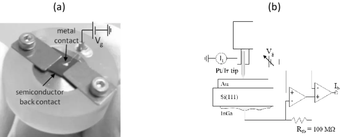
1.2.3 Implementation of BEEM
Implementing BEEM on our STM setup has required the fabrication of a new sample holder providing two isolated contacts for the metal and the semiconductor terminals (Figure 7a). Apart from the sample holder, a specific current amplifier was developed for the measurement of the BEEM current IC (Figure 7b).
(a) (b)
Figure 7 : (a) BEEM sample holder. (b) Schematics of the BEEM connections and current measurement setup.
27
In the configuration that we have chosen, the tunneling current is measured on the tip terminal with respect to ground. The tunneling barrier bias voltage is applied to the metal contact. The BEEM current amplifier is thus referenced to the voltage applied to the metal layer. A differential amplifier subtracts the tunneling barrier voltage to the output of the current amplifier. The BEEM current amplifier uses an OPA111 operational amplifier with a feedback resistance Rfb of 100 M for current-voltage conversion. The differential amplifier has three gains from 1 to 100. This circuit has an adjustable offset voltage Voff. Simultaneous topography, tunneling and ballistic currents measurements can be performed.
BEEM experiments are performed following two modes.
- The image Mode. For a given electron energy, the STM tip scans the sample surface at a constant height. For each (x,y) spatial position of the tip, It and Ic are recorded to give a cartography of the electron transmission at the interface metal/semiconductor.
- The spectroscopy Mode. For a fixed position of the tip, the variation of Ic is measured versus the tunneling bias voltage Vgap. The tunneling current It is kept constant by the feedback loop controlling the tunnel gap.
1.2.4 Luminescence detection setup
To perform STL measurements, we couple an optical spectroscopy setup to the microscope (Figure 8).
Figure 8 : Schematics of the luminescence spectroscopy setup. A beam splitter and a 658 nm laser are used for the optical alignment by in-situ photoluminescence spectroscopy. During the STL measurements, the electrons are injected from the tip and the luminescence from QW is collected on the backside of the sample. The characteristics of lens 1 used for collecting the luminescence light are f = 18.4 mm, NA = 0.27 and those of lens 2 used for focusing on the spectrometer slit are f = 75 mm, NA = 0.08.
28
This luminescence setup includes a laser excitation source at 658 nm for in-situ photoluminescence (PL) spectroscopy measurements. Accordingly the PL signal can be optimized prior to electron injection from the tip without modifying the position of the sample inside the cryostat. The laser beam excites the sample from the backside thanks to a beam splitter which attenuates by about 35 % the 658 nm laser source while ensuring an almost full transmission in the emission range of the QW’s (Figure 9a). A short focal lens (lens 1) located in the cryostat is used to collect the light coming out of the sample. A second lens (lens 2) focuses the luminescence onto the inner monochromator slit. The numerical aperture (NA) of lens 2 almost matches the aperture of the monochromator blazed at 1 µm.
(a) 600 700 800 900 1000 0 20 40 60 80 100 Transmission (%) Wavelength (nm) (b) 300 400 500 600 700 800 900 1000 1100 0,1 1 External quantum effic ienc y (%) Wavelength (nm)
Figure 9 : (a) Beam splitter transmission versus wavelength. (b) Typical spectral response of the Ag-Cs-O photocathode.
The QW InGaAs alloy composition was chosen so to keep the QW’s emission wavelength below 1 µm. In this spectral range, we can use as photon counting device a photomultiplier tube (PMT) equipped with a Ag-Cs-O photocathode which exhibits a quantum efficiency of typically 10-3 (Figure 9b). For measuring the luminescence spectrum, we use a Jobin Yvon H25 Monochromator (NA = 0.25, 2 mm wide slits, 600 groove/mm diffraction grating, spectral resolution +/-1.5 nm). We work with the first order of diffraction of the grating.
30
1.3 Results
1.3.1 BEEM of Au/n-Si junctions
For testing our BEEM setup we have studied archetype Au/Si-n junctions. Gold deposition on the clean (111) Si surface is achieved by electrochemistry using a gold chloride solution. Samples are then cleaved in order to obtain small contact surface about 4 mm2. The current-voltage characteristics are first measured to determine the Schottky barrier height. Density current-voltage (J-V) curves of Au(250 nm)/Si-n and Au(350 nm)/Si-n samples are shown in Figure 10. The Schottky barrier height can be deduced from the analysis of these curves. We start from the following formula, which gives the current density J running through the biased junction as a function of the applied bias V [Rhoderik1988] :
𝐽 = 𝐽𝑠𝑎𝑡(1 − 𝑒−𝑒𝑉 𝑘𝑇⁄ ) = 𝐽𝑠𝑎𝑡𝑒−𝑒𝑉 𝑘𝑇⁄ (𝑒𝑒𝑉⁄𝑘𝑇− 1)
where Jsat is the saturation current.
-0,8 -0,6 -0,4 -0,2 0,0 0,2 0,4 0,6 10-2 10-1 100 101 102 103 104 Au(250 nm)/Si-n Au(350 nm)/Si-n Au(10 nm)/Si-n J ( µA/c m 2 ) V (V)
Figure 10 : Current density-voltage characteristics of Au(250 nm)/Si-n (red squares) and Au(350 nm)/Si-n (green triangles circles) and Au(10 nm)/Si-n (black circles).
Then we introduce the ideality factor n, which originates from the barrier dependence on applied voltage :
31
𝐽𝑠𝑎𝑡 = 𝐴∗𝑇2𝑒−Φ𝑏⁄𝑘𝑇 𝐴∗= 4𝜋𝑒𝑘 2𝑚 𝑒 ∗ ℎ3where b is the Schottky barrier height, A* = 2.58 x 10⁸ µA m-2 K-2 is the Richardson constant for Si(111).
Then, from the current density-voltage characteristics one can plot the Rhoderick function : 𝑅ℎ(𝑉) = ln ( 𝐽 𝐴∗𝑇2(𝑒𝑒𝑉⁄𝑘𝑇−1)) = − 𝑒Φ𝑏 𝑘𝑇 − 𝑒𝑉 𝑛𝑘𝑇 = 𝛼 + 𝛽𝑒𝑉.
Rh(V) can be fitted by a linear function in the saturation region (Figure 11):
-0,4 -0,2 0,0 0,2 0,4 0,6 -50 -45 -40 -35 -30 -25 -20 Au(10 nm)/Si-n Au(250 nm)/Si-n Au(350 nm)/Si-n Rh Bias (V)
Figure 11 : Rh function of Au(250 nm)/Si-n (red squares), Au(350 nm)/Si-n (green triangles) and Au(10 nm)/Si-n (black circles)
Two quantities can be extracted from the Rh curve fitting : the barrier height and the ideality factor n. The values obtained for the ideality factor (Table 1) shows that the Au/Si-n structures exhibits a strong rectifying character. The value of the barrier height is between 0.7 eV and 0.76 eV which is comparable with published values. The electrical characteristics of these Au/Si-n structures thus appear to be suitable for BEEM measurements.
32
Table 1 : Results of Rh-function linear fit. The extracted fitting parameters, and, and the deduced values of b and n are reported. The dynamic resistance of the unbiased junction is also indicated.
sample Intercept α Slope β Barrier height B (eV) Ideality factor n Dynamic resistance (Ω·cm2) Au(10 nm)/Si -29,66 -39,94 0.76 0.97 16·103 Au(250 nm)/Si -27,14 -37,03 0.7 1.05∓0.09 140 Au(350 nm)/Si -29,59 -37,17 0.76 1.04∓0.08 27·103
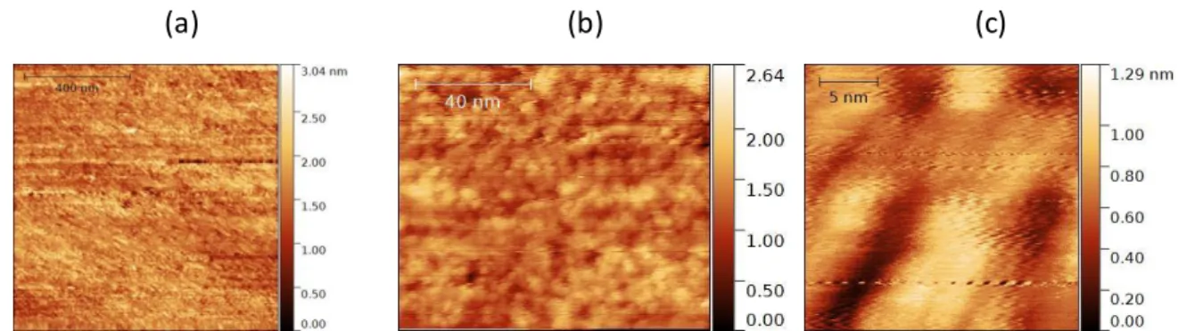
Figure 12 shows an example of an STM topography image of the gold surface of Au/Si-n structure. The metallic layer is formed by the coalescence of flat Au islands of 50 nm typical size and exhibits cavities with typical size of 20 nm. This morphology is confirmed by AFM measurements.
Figure 12 : STM image of the Au(4 nm)/Si-n surface. The Au layer is deposited by electrochemical process. The scan size is 1 x 1 µm2; the gap voltage Vg is 0.7 V; the tunneling current It is 1.5 nA and is maintained constant by the feedback loop.
We have performed BEEM experiments on these junctions. Figure 13 shows the variation of the ballistic electron transmission Ib/It as a function of the bias applied to the tunneling junction. This excitation spectroscopy measurement is performed at constant tunneling current. In this case, tip-sample distance and, consequently, tunneling transmission change. We successively measured the transmission spectrum for different values of It =3, 6 12, 14, 20 and 32 nA. We find that the transmission does not depend on the values of the tunneling current.
The onset of the transmission is found at an injection bias potential of 0.67 V which is in reasonable agreement with the barrier height value deduced from the analysis of the junction electrical characteristics. However, the variation of the transmission above the onset does not follow the power law predicted by the Bell-Kaiser or Ludeke-Prietsch models.
33
A power law with an exponent of 1.2 fits quite well the experimental curve, but this exponent is well below the values of 2 or 2.5 predicted by the above mentioned models.
0,2 0,4 0,6 0,8 1,0 1,2
1E-4 1E-3 0,01 0,1
Average Ib/It from 3, 6, 12, 14, 20, 32 nA Bell-Kaiser (n=2); barrier = 0,41 Ludeke-Prietsch (n=2,5); barrier = 0,39 n=1,2; barrier = 0,67 eV
Average transmissi
on
Tunneling voltage (V) Average Ib/It nFigure 13 : Average transmission Ib/It measured on the Au/Si-n sample as a function of the tunneling bias voltage. Tip position is fixed during the experiments. Tunneling current is maintained constant during the voltage scan. Error bars are standard deviations. Experiment is performed at room temperature. Various power law fittings are shown.
In order to measure the variation of the transmission as a function of tip position, we have performed BEEM imaging. For each measurement the bias voltage applied to the tunneling barrier is fixed at 1.1 V. Measurements are performed for different values of the tunneling currents : 9, 14, 20 and 30 nA. The comparison between STM topography images and ballistic-tunneling current ratio (Ib/It) images is presented in Figure 14.
STM topography image does not change with increasing tunneling current. Note that no surface modification is observed during the scan. For the highest values of It, the contrast in the transmission image is improved and additional features are revealed. There are some spots where the transmission reaches 10% while very weak ballistic electron transmission channels are observed in the interstices between Au islands. The flat Au islands height changes by about one gold atomic layer. However, the signal-to-noise ratio on the transmission measurement presented here is not sufficient to detect a correlation with the island thickness from which could be deduced the electron mean free path.
These images however demonstrate the capability of our experimental setup for BEEM measurements on metal/semiconductor structures.
34
It STM topography Ib/It 9 nA 14 nA 20 nA 30 nAFigure 14 : Simultaneously recorded STM (left) and BEEM (right) images of a Au/Si-n sample for different values of It. The gap voltage is Vg = 1.1 V. The acquisition time of each image is 10 min.
35
1.3.2 Optical detection of BEEM in Pd/Fe/GaAs/InGaAs/GaAs structures
The sample used for the optical detection of ballistic electron transmission is a structure which has already allowed evidencing spin-filter effect from the cathodoluminescence emitted under injection of a free spin-polarized electron beam [Li2014]. This sample consists of a semiconductor heterostructure, MBE-grown at the Institute of Semiconductor Physics, Novosibirsk [3246 (VS1-47)], on top of which a 4 nm-thick iron layer capped with a 2 nm-nm-thick palladium layer was grown in LPMC by thermal evaporation in UHV conditions. The Fe growth on the clean (100) GaAs surface is known to be epitaxial so that continuous ferromagnetic films of a few nm thickness can be obtained this way. The 2 nm-thick Pd cap protect efficiently the iron layer from oxidation. The whole structure, referred to as InGaAs_1 sample in the following, is detailed in Figure 15.
- Pd (2nm) - Fe (4nm) - p-GaAs:Be (7×1017cm-3) (10nm) - p-In0.18Ga0.82As:Be (7×1017 cm-3) (10nm) - p-GaAs:Be (7×1017 cm-3) (20nm) - p-In0.18Ga0.82As: Be (7×1017 cm-3) (10nm) - p-GaAs:Be (7×1017 cm-3) (20nm) - p-Al0.3Ga0.7As:Be (7×1017 cm-3) (40nm) - n-GaAs:Si (2×1018 cm-3) (100nm) - n+-GaAs(100) substrate
Figure 15 : (left) Schematics of the GaInAs_1 sample band diagram in real space. (right) structure composition is indicated from cap layer to substrate.
Fe grows epitaxial onto GaAs when deposited by MBE at room temperature [Filipe1997]. As a consequence, very thin continuous magnetic films can be obtained. Figure 16 shows the constant current STM topography image of the cap Pd layer. The topography is monitored at different scales. The RMS surface roughness does not exceed 1 nm as expected for 2D epitaxial layers.
36
(a) (b) (c)
Figure 16 : Constant tunneling current STM image of the Pd surface of the Pd/Fe/GaAs sample. Scan size, tunneling current and gap voltage are respectively (a) 1000 nm, 1.43 nA and 0.7 V, (b) 100 nm, 0.94 nA and 0.6 V, (c) 23 nm, 0.94 nA and 0.7 V.
To identify the QW’s light emission, PL measurements are performed inside the cryostat at room temperature. The 658 nm laser beam illuminates the back side of the sample. The PL spectrum (Figure 17) exhibits an intense broad peak located at 860 nm which corresponds to the GaAs bulk emission and a weak contribution of the QW’s emission around 960 nm (cf. inset in Figure 17).
800 820 840 860 880 900 920 940 960 980 1000 0 1x10⁵ 2x10⁵ 3x10⁵ 4x10⁵ 5x10⁵ 6x10⁵ 920 940 960 980 1000 3x10⁴ 4x10⁴ 5x10⁴ Intensity (counts/s) Wavelength (nm) Intensit y ( counts/ s) Wavelength (nm)
Figure 17 : Photoluminescence spectrum from the InGaAs_1 sample excited and detected from the backside. The excitation wavelength is 658 nm. A weak contribution of the InGaAs QWs located at 100 nm from the metal/GaAs interface is detected.
The weakness of the QWs photoluminescence signal is due to the fact that the sample is excited from the backside with a wavelength well above the GaAs bandgap . Therefore, the excitation light is all absorbed close to the back substrate surface. The QWs are populated with conduction electrons only by the residual absorption of the GaAs
37
luminescence that reaches the other side of the sample. Note that, at high wavelengths, a large background is still measured (104 counts/s), which arises from the emission of the heavily doped GaAs substrate. In consequence, is it impossible to evaluate precisely the efficiency of the electron capture and recombination in the QW’s.
After having selected an area of minimal roughness, we inject electrons from the tip with a tunneling barrier bias larger than the GaAs band gap and measure the luminescence spectrum in the range corresponding to the QW emission. This experiment is performed for three different sets of injection parameters : It = 14 nA, Vg = 1.5 V, It = 26 nA, Vg = 1.7 V and It = 36 nA, Vg = 2 V. The result is shown in Figure 18. No light emitted from the QW’s is detected around 960 nm, whatever the tunneling current. The slight increase in the signal measured for It = 26 nA and Vg = 1.7 V is probably due to a slight warming of the PMT, given the time required for recording the spectra with a good statistics.
900 920 940 960 980 1000 0 20 40 60 80 Wavelength (nm) Countin g rate (counts/s) It = 26nA ; Vg=1,7 V It = 14.4 nA ; Vg = 1.5 V It = 36nA; Vg=2 V
Figure 18 : Luminescence spectrum measured on the Pd/Fe/GaAs/InGaAs/GaAs sample under tunneling injection of electrons above the GaAs bandgap. The injection conditions are : It = 14.4 nA, Vg = 1.5 V (black squares), It = 26 nA, Vg = 1.7 V (empty red circles) and It = 36 nA, Vg = 2 V (blue triangles).
1.3.3 Luminescence of GaAs/InGaAs/GaAs QW's structures
Several intrinsic factors can limit the magnitude of the optical signal coming out from the back side of the sample sitting into the cryostat :
- the electron transmission efficiency through the metal layer and Schottky contact, - the efficiency of the electron capture by the QW which depends on the minority carrier transport properties between the entrance interface and the QW,
38
- the quantum yield of the radiative recombination process in the QW, - the light extraction from the semiconductor,
- the numerical apertures of the collection optics and of the monochromator, - the photon detector efficiency.
To evaluate the actual reasons for the absence of luminescence signal from the quantum wells under injection of electrons from the tip, we performed the same experiment on bare GaAs/InGaAs/GaAs samples without any metal layers on top. Two specific samples were grown which are described in Table 2.
The active region of these samples is moderately p-doped (Be concentration : 4 x 101 6 cm-3) and incorporates a set of three InGaAs QWs separated by GaAs barriers. The two structures differ one from each other by the thickness of the GaAs top layer which determines the position of the InGaAs QWs from the surface. In the 3720 sample, the thickness of the top GaAs layer is larger than the band bending region near the surface while in the 3721 sample the GaAs top layer is thinner than the band bending region and the QWs are partially located in the electric field of the depletion region.
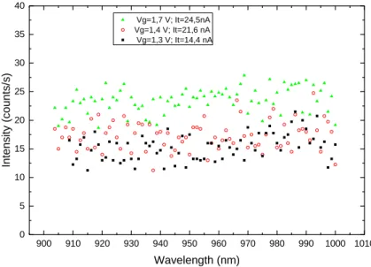
We performed STM-excited luminescence on these 3720 and 3721 samples. Figure 19 shows the luminescence spectra of the 3721 sample recorded at different bias Vg and tunneling currents. Again no signal is detected in the wavelength range corresponding to the QW’s emission. Therefore, the weak electron transmission through metal/semiconductor junction cannot be evoked to explain the absence of luminescence signal. The reason might be the small optical efficiency of our optical detection system.
Table 2 : Structure of GaAs samples with embedded InGaAs QWs.
Sample 3720 115 nm Sample 3721 40 nm p-GaAs : Be 4·1016 10 nm p-GaAs : Be 4·1016 3 times 7 nm p-In0.18Ga0.82As:Be 4·1016 - QW 125 nm p-GaAs : Be 4·1016 30 nm p-Al0.3Ga0.7As : Be 4·1016 300 nm p-GaAs : Be 4·1018 Buffer 350 µm Substrate p-GaAs(001) Wt 19524/Zn
39
900 910 920 930 940 950 960 970 980 990 1000 1010 0 5 10 15 20 25 30 35 40 Vg=1,7 V; It=24,5nA Vg=1,4 V; It=21,6 nA Vg=1,3 V; It=14,4 nA Int en sity (co un ts/s) Wavelength (nm)Figure 19 : STM-excited luminescence of sample 3721 (GaAs (40 nm) / GaInAs QW’s). Tip position is fixed during all scan and the tunneling current is maintained constant.
Even extending the detection to the GaAs emission range, no luminescence signal is detected (Figure 20). 800 820 840 860 880 900 920 940 960 980 1000 0 10 20 30 40 50 60 70
80 Sample 3721, high pass filter 780 nm, Vg = 1.8V, It = 29 nA 4 pts smoothing Int en sity (co un ts/s) A
Figure 20 : STM-excited luminescence from the 3721 sample (GaAs (40 nm) / GaInAs QW’s). Tip position is fixed for the whole data. Tunneling current is maintained constant. Electrons are injected from the tip with It = 29 nA and Vg = 1.8 V. The acquisition time for each point is 6s and total acquisition time is 960 s. Vertical lines mark the respective positions of the QW’s (953 nm) and GaAs (867 nm) luminescence peaks.
40
One explanation for the absence of STM-excited luminescence in all studied samples could be the poor optical efficiency of our optical detection system. In order to determine the efficiency of our optical spectroscopy system and of the capture and recombination in the InGaAs QW structures, we have performed photoluminescence measurements.
PL spectra of the bare GaAs/InGaAs/GaAs-p sample, recorded for optimized (blue cirve) and non-optimized light collection, are shown in Figure 21. The 658 nm laser is used for excitation. The sample was oriented “up-side-down” in order to absorb light in the region where the QWs are located. The peaks located at 870 nm and at 940 nm correspond to PL of the GaAs and of the QW’s respectively. After optimization of the QW’s signal, the peak counting rate is close to 104 photon/s. With an excitation power of about 1 mW, a rough estimate of the QW’s photoluminescence yield is 10-12 to 10-11. If we assume that similar yield can be expected when injecting electrons with the STM tip, one would get a photoluminescence yield of about 1 photon/s for an injected current of 10 nA. Taking into account a light extraction coefficient of ~ 10-2 from the GaAs of refractive index nGaAs ~ 3.5 and the S1 cathode efficiency of 10-3 the overall efficiency of our light collection and analysis system is of the order of 10-6 which is clearly not sufficient to detect STM-induced luminescence. 780 800 820 840 860 880 900 920 940 960 980 1000 0 10000 20000 30000 40000 50000 60000 70000 Counts (counts/s) Wavelength (nm) optimized spectrum complete spectrum
Figure 21 : Photoluminescence spectra of the 40 nm GaAs/GaInAs sample inside the cryostat. (Blue curve) optimized spectrum in the QW’s emission range. (Inset) Schematics of the experiment excitation and detection configuration. Excitation wavelength : 658 nm.
QW
Exc.
41
In the above estimate, the efficiency of the electron capture by the QWs is not evaluated. In a photoluminescence experiment, it is strongly dependent on the excitation wavelength through the absorption coefficient. We have thus performed a photoluminescence study of the GaAs/InGaAs samples for different excitation wavelengths : UV (360 nm), Red (632.8 nm and 658 nm), IR (780nm and 840 nm). In such way we probe the luminescence from the QWs when carriers are excited over different depths in the sample (see the absorption lengths reported in Table 3 for different wavelengths).
Table 3 : Absorption length in intrinsic GaAs for different light wavelength. The bold line corresponds to the distance between QW and the surface.
Laser wavelength (nm) 360 632.8 658 780 840
Laser energy (eV) 3.45 1.97 1.88 1.59 1.48
Absorption length (nm) 12.5 50 350 1000 1000
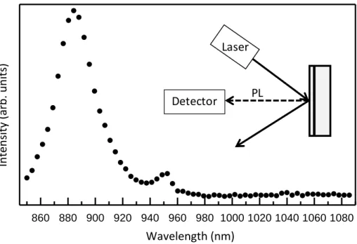
Starting with the 3720 sample, the PL spectrum measured in reflection geometry for 844 nm light excitation is shown in Figure 22. Two luminescence peaks are observed: the main contribution at 884 nm corresponds to the recombination at the GaAs bandgap and the satellite contribution at 952 nm originates from the QW’s luminescence.
860 880 900 920 940 960 980 1000 1020 1040 1060 1080 In te n sity (arb . u n its) Wavelength (nm)
Figure 22 : PL spectrum of Sample 3720 in reflection configuration for an excitation wavelength of 844 nm. Two peaks are observed : at 884 nm (bulk GaAs) and 952 nm (QW).
Detector PL
42
In the transmission geometry, which corresponds to the configuration of electron injection set-up and for an IR excitation, we better discriminate between the previously dominant 884 nm peak and the QW’s peak. In this geometry, the luminescence light corresponding to the recombination through the GaAs gap is filtered out by the absorption through the GaAs substrate. As a result, the luminescence spectrum of the 3720 sample (Figure 24, red symbols) reveals the presence of two resolved peaks of equivalent intensities at 917 nm and 953 nm. The peak at 953 nm corresponds to the QWs emission while the peak at 917 nm corresponds to the low energy tail of the GaAs emission which is spectrally filtered by the re-absorption in the GaAs substrate with a cut-off around 900 nm. Therefore, the light emitted from the recombination in the QW’s is transmitted through the substrate, which strengthens our experimental approach of injecting electron from the topside of the sample and detecting the emitted light from the backside of the sample. In the same measurement conditions, the sample 3721 (with QW’s located at 40 nm from the surface) only shows a very weak QWs contribution at 953 nm (Figure 23, black symbols).
840 860 880 900 920 940 960 980 1000
Intensity (arb. units)
Wavelength (nm)
40nm p-type GaAs (3721), PL from IR(780 nm), transmission, laser on face 115 nm p-type GaAs (3720), PL from IR(780 nm), transmission, laser on face
Figure 23 : PL spectra in transmission geometry of 3720 (red symbols) and 3721 (black symbols) samples for an excitation wavelength of 780 nm (experimental configuration is schematized in the inset). The 3721 sample has a 40 nm p-type top GaAs layer and the 3720 sample has a 115 nm p-type top GaAs layer. The spectra are normalized to the peak intensity at 917 nm. An interferential filter is used for cutting-off the laser light at 780nm.
Exc.
43
For better evidencing the QWs contribution in the 3721 samples, we have performed a transmission PL experiment exciting the sample from the backside (Figure 24, blue symbols). In this geometry, the QW’s luminescence is weaker since it is only excited by the residual luminescence light corresponding to the recombination through the GaAs bandgap and transmitted through the whole sample. The slight difference between the two spectra in the range between 940 nm and 960 nm is due to the QWs luminescence.
840 860 880 900 920 940 960 980 1000
Intensity (arb. units)
Wavelength (nm)
40nm p-type GaAs (3721), PL from IR(780 nm), transmission, laser on bottom 40nm p-type GaAs (3721), PL from IR(780 nm), transmission, laser on face
Figure 24 : (a) PL spectra in transmission geometry of 3721 sample for an excitation wavelength of 780 nm coming from the backside (blue symbols) and the topside (black symbols) of the sample (corresponding illumination configurations are shown in the inset). The spectra are normalized to the peak intensity at 917 nm. An interferential filter is used for cutting-off the laser light at 780nm.
When exciting with UV light at 375 nm, i.e. when the absorption length is smaller than the band bending region which mimics quite reasonably the injection with a tip, the GaAs emission vanishes and QW’s emission line at 950 nm is by far more intense (Figure 25).
Exc.
Det.
Exc.
44
840 860 880 900 920 940 960 980 1000 1000 2000 3000 4000 5000 6000115 nm p-type GaAs, sample 3720, UV laser, PL
Counting rate (count/s)
Wavelength (nm)
Figure 25 : Transmission PL spectrum of 3720 sample for an excitation at 375 nm.
From this study, it appears that 3720 sample, with QWs out of the depletion region , provides the largest QW’s luminescence contribution. Moreover, QW’s photoluminescence is observed with similar intensities in both reflection and transmission geometries so that our STL spectroscopy configuration is in principle well adapted for the targeted measurements. It remains that the overall light collection and detection efficiency of our system is not sufficient to allow STL measurements.
Exc.