Additive manufacturing of patterned 2D
semiconductor through recyclable masked growth
The MIT Faculty has made this article openly available.
Please share
how this access benefits you. Your story matters.
Citation
Guo, Yunfan et al. "Additive manufacturing of patterned 2D
semiconductor through recyclable masked growth." Proceedings of
the National Academy of Sciences 116, 9 (February 2019): 3437-3442
© 2019 National Academy of Sciences
As Published
http://dx.doi.org/10.1073/pnas.1816197116
Publisher
National Academy of Sciences (U.S.)
Version
Final published version
Citable link
https://hdl.handle.net/1721.1/121495
Terms of Use
Article is made available in accordance with the publisher's
policy and may be subject to US copyright law. Please refer to the
publisher's site for terms of use.
Additive manufacturing of patterned 2D semiconductor
through recyclable masked growth
Yunfan Guoa, Pin-Chun Shena, Cong Sub, Ang-Yu Lua, Marek Hempela, Yimo Hanc, Qingqing Jia, Yuxuan Lina, Enzheng Shid, Elaine McVaya, Letian Doud, David A. Mullerc, Tomás Palaciosa, Ju Lib, Xi Linge,f,g,1, and Jing Konga,1
aDepartment of Electrical Engineering and Computer Science, Massachusetts Institute of Technology, Cambridge, MA 02139;bDepartment of Nuclear and Materials Science and Engineering, Massachusetts Institute of Technology, Cambridge, MA 02139;cSchool of Applied & Engineering Physics, Cornell University, Ithaca, NY 14850;dDavidson School of Chemical Engineering, Purdue University, West Lafayette, IN 47907;eDepartment of Chemistry, Boston University, Boston, MA 02215;fDivision of Materials Science and Engineering, Boston University, Boston, MA 02215; andgThe Photonics Center, Boston University, Boston, MA 02215
Edited by Ramamoorthy Ramesh, University of California, Berkeley, CA, and accepted by Editorial Board Member Zachary Fisk January 12, 2019 (received for review September 18, 2018)
The 2D van der Waals crystals have shown great promise as potential future electronic materials due to their atomically thin and smooth nature, highly tailorable electronic structure, and mass production compatibility through chemical synthesis. Elec-tronic devices, such as field effect transistors (FETs), from these materials require patterning and fabrication into desired struc-tures. Specifically, the scale up and future development of “2D”-based electronics will inevitably require large numbers of fabrica-tion steps in the patterning of 2D semiconductors, such as transifabrica-tion metal dichalcogenides (TMDs). This is currently carried out via mul-tiple steps of lithography, etching, and transfer. As 2D devices become more complex (e.g., numerous 2D materials, more layers, specific shapes, etc.), the patterning steps can become economi-cally costly and time consuming. Here, we developed a method to directly synthesize a 2D semiconductor, monolayer molybdenum disulfide (MoS2), in arbitrary patterns on insulating SiO2/Si via seed-promoted chemical vapor deposition (CVD) and substrate en-gineering. This method shows the potential of using the prepat-terned substrates as a master template for the repeated growth of monolayer MoS2patterns. Our technique currently produces arbi-trary monolayer MoS2patterns at a spatial resolution of 2μm with excellent homogeneity and transistor performance (room temper-ature electron mobility of 30 cm2V−1s−1and on–off current ratio of 107). Extending this patterning method to other 2D materials can provide a facile method for the repeatable direct synthesis of 2D materials for future electronics and optoelectronics.
2D semiconductor
|
monolayer MoS2|
patterned growth|
growth mechanism|
recyclable masked growthI
n recent years, the family of monolayer transition metal dichal-cogenides (TMDs) has become attractive semiconducting crystals for nano- and flexible electronics due to their atomic thinness, high carrier mobility, and excellent flexibility (1, 2). In addition, TMDs have drawn considerable attention in condensed matter due to the unique electronic band structures and intriguing valley–spin cou-pling, making them promising for valleytronics (3), piezoelectrics (4), bandgap modulation (5), and high-quantum efficiency optical/ optoelectronic applications (6, 7).To fabricate future 2D-based electronics and optoelectronics structures, it is necessary to pattern 2D materials for contacts, gating, optical access, etc. (8, 9). At present, patterning TMDs have relied on either subtractive or additive manufacturing.“Growth and etch” (10–12) is perhaps the most typical method of 2D patterning, where it utilizes subtractive manufacturing (akin to“top down”) to lithographically define and subsequently etch away unwanted areas of 2D material. This method has spatial resolution roughly down to nanometers (when using electron beam lithography), but it has a high manufacturing cost and can become time consuming. Addi-tionally, the inevitable generation of multiple layers (which is nec-essary when constructing an integrated system) becomes difficult to handle, as selective etching of 2D materials still poses fabrication
challenge (also due to their atomic thinness). Furthermore, con-taminations between interfaces and rough, amorphous edge termi-nations may be introduced during fabrication, thus increasing the chance for quality deterioration of as-grown materials. To avoid surface contamination by resist residues, shadow mask (13) and laser cutting (14) can be considered, but the poor spatial resolutions typically are in the range of near millimeters to hundreds of micrometers.
However, for additive manufacturing (“bottom-up”) techniques, inkjet printing (15) has been extensively used for the large-scale preparation of TMD patterns. Nevertheless, it requires solution-based 2D flakes (typically multilayered), and the minimal feature size is usually larger than 10μm. Various efforts have been devoted to prepattern seed precursors [molybdenum oxide (MoO3),
am-monium heptamolybdate (16), or Au catalyst (17)] to generate patterned TMD structures directly, although preventing multilayer islands growing on monolayer regions still turned out to be chal-lenging. Substrate modification by O2plasma provides a simpler
route to patterned TMDs (18, 19), but the reported electrical mo-bility has been two orders of magnitude lower than as-grown TMDs (1 cm2V−1s−1) with poor spatial resolution (∼100 μm).
Significance
Traditional semiconductor fabrication methods, such as lithog-raphy and etching, have been sufficient for the needs of in-tegrated circuits over past decades. Their applicability has also been demonstrated in emerging 2D materials, which offers facile processing over large lateral dimensions, while unique and remarkable properties due to the confinement within atomic thicknesses. Nevertheless, each fabrication step adds cost to the manufacturing and increases the possibility of quality degradation. Here, we developed a method to directly synthesize arbitrary monolayer molybdenum disulfide pat-terns with high spatial resolution, excellent homogeneity, and
electrical performance on insulating SiO2/Si. Significantly, our
on-demand method allows for the repeated growth of pat-terned 2D materials with preserved structural integrity and material qualities, paving the way for simpler and cost-effective fabrication.
Author contributions: Y.G. and J.K. designed research; Y.G., P.-C.S., C.S., A.-Y.L., M.H., Y.H., and E.M. performed research; Y.G., P.-C.S., C.S., Q.J., Y.L., E.S., L.D., D.A.M., T.P., J.L., X.L., and J.K. analyzed data; and Y.G., P.-C.S., C.S., and J.K. wrote the paper. The authors declare no conflict of interest.
This article is a PNAS Direct Submission. R.R. is a guest editor invited by the Editorial Board.
Published under thePNAS license.
1To whom correspondence may be addressed. Email: [email protected] or [email protected].
This article contains supporting information online atwww.pnas.org/lookup/suppl/doi:10.
1073/pnas.1816197116/-/DCSupplemental.
Published online February 12, 2019.
ENGINEER
Herein, through in-depth studies of the growth mechanism and precursor control, we have found that plasma-based substrate modification can be used to directly grow patterned monolayer molybdenum disulfide (MoS2) with high crystal quality, diverse
geometries, high spatial resolution (2μm at present, limited by laser lithography), and high electrical mobility (∼30 cm2 V−1 s−1) on
SiO2/Si substrate. The same patterning mask can be recycled for
repeated growth with consistent material morphology and quality each time, which demonstrates the potential of this method for a “master–replica” type of repeated manufacturing. Such an additive manufacturing method opens up the possibilities for wide applica-tions of 2D TMD nanostructures in modern electronics and opto-electronics with much simpler fabrication.
Results and Discussions
Substrate modification is the first step to achieve the patterned MoS2structures as shown in Fig. 1A. As a proof of concept, we
have chosen to define MoS2 in the shape of kirigami patterns.
Traditionally, kirigami is a technique to create 3D structures from 2D sheets and has been applied in 2D materials to build robust macro- or microscale structures with tunable mechanical properties (20–22). Photolithography defines patterns of photo-resist on the substrates (SI Appendix, Fig. S1) while undeveloped areas are etched away using O2 plasma, which simultaneously
modifies the surface of SiO2 substrate. After removing the
de-veloped photoresist, MoS2can selectively grow on plasma-treated
areas, similar to our previous studies (details are in Methods) (23, 24). As the plasma treatment creates a region with higher surface energy and enhanced hydrophilicity (discussion below), the hydro-philic salt perylene-3,4,9,10-tetracarboxylic acid tetrapotassium
(PTAS) is used to promote seeded, selective MoS2growth only at
the O2plasma-treated areas, forming as-grown patterned MoS2.
Inspection of the resultant growth using optical microscopy (OM) clearly shows a patterned growth of MoS2(in the shape of
a wave array) on SiO2/Si (Fig. 1B). The reflectance contrast of
the green-tinted MoS2, which comprises the wave, is uniform,
with a strap width of 20μm (tunable by changing the patterns on the substrate). Fig. 1C shows that MoS2grows at opposite
lo-cations (in contrast to Fig. 1B) when a negative photoresist was used for the same pattern. Through this technique, monolayer MoS2patterns with diverse morphologies and different feature
sizes can be obtained by only changing the original growth “mask” (SI Appendix, Fig. S2 A1–C2). Currently, the minimal spatial resolution is 2 μm, which is limited by the direct laser writing instrument (SI Appendix, Fig. S2 D1 and D2). To evaluate the surface morphology of the MoS2 patterns, we use atomic
force microscopy (AFM). We first observed that the strong O2
plasma etching causes a height difference between the pristine SiO2regions and the etched regions of about 2 nm (SI Appendix,
Fig. S3A). After the growth of MoS2, a flat and pristine
mono-layer fills in the recessed region (Fig. 1D) and reduces the height difference to∼1.3 nm (SI Appendix, Fig. S3B), confirming that the thickness of MoS2patterns is monolayer (∼0.7 nm).
To evaluate the crystallinity of the monolayer MoS2patterns,
characterizations with photoluminescence (PL) and Raman spectroscopy were carried out. A strong PL emission at around 1.85 eV with an FWHM intensity of about 60 meV was observed on all tested samples, consistent with the emission of grown monolayer MoS2(Fig. 1G) (25). For Raman spectroscopy, the
frequency difference between Raman peaks located at 383 cm−1
Preferential Growth (3) Modified Substrate (1) 100 m SiO2 MoS2 100 m SiO2 MoS2 SiO2 MoS2 5 m 10 nm -10 nm (2)
A
B
C
D
5 15 25 35 45 10 20 30 40 0.5 1 0 1.5 2 0 0 5 15 25 35 45 55 1.0 0.9 0.8 0.7 0.6 0.5 10 20 30 40 0E
Energy (eV) Intensity (a.u.) 1.7 1.8 1.9 2.0 1.85 eVG
360 380 400 420 440 Raman Shift (cm-1) Intensity (a.u.) E2g A1g 21 cm-1H
1 nm -20 0 20 40 Back-gate Voltage Vbg (V) 40 30 20 10 0 Current I ds ( A) 10-6 10-8 10-10 10-12 Current I ds (A) 20 mI
J
0 1 2 3 4 5 Channel Length Lch ( m) 1 m 2 m 3 m 4 m Au Ni Si (P+) MoS2 SiO2 1600 900 600 300 1200 0 Rtot (k . m)F
Length ( m) Length ( m) *104 Intensity (a.u.) *104 Intensity (a.u.) Length ( m) Length ( m) pristine SiO2/Si growth precursors PTAS Seed treated region Selective-area Modification patterned photo-resist pristine SiO2/Si O2 plasma remove photo-resist CVD growthFig. 1. Patterned growth and characterization of MoS2nanostructures. (A) Schematic representation of the procedures for the direct growth of MoS2 nanostructures via seed-promoted growth and sub-strate engineering. Step 1: the selective-area modi-fication process by lithography patterning and O2 plasma etching; step 2: the patterned regions are distinguished from pristine SiO2/Si substrates after modification; step 3: the preferential growth of MoS2on patterned SiO2/Si regions. (B) A typical OM image of a monolayer MoS2 wave array. (C) OM image of a monolayer MoS2wave film that grows at the opposite locations when a negative photoresist was used for the wave pattern in B. (D) AFM image of a monolayer MoS2kirigami structure showing the flat surface and ordered edge morphology. (E and F) PL mappings for monolayer MoS2wave arrays and the inversed wave film pattern. (G) A typical PL spectrum collected on the monolayer MoS2 wave structures. (Inset) A typical Raman spectrum collected on the monolayer MoS2wave structures. (H) ADF-STEM image of a patterned monolayer MoS2edge showing the clean and ordered edge at atomic scale. (I) Transfer (Ids− Vbg) characteristic of a typical back-gated transistor fabricated on our CVD-patterned MoS2film with gate voltages from−30 to 50 V and a bias Vdsfixed at 1 V. The room temperature elec-tron mobility of the transistor is 29.3 cm2V−1s−1. The red curve shows the transfer characteristic of the same MoS2transistor in logarithmic scale. The on–off current ratio is∼107. (Inset) Optical image of a typical MoS2device based on the wave pattern. (J) Total device resistance RTOT normalized by width vs. channel length Lchmeasured at a carrier concentra-tion n of∼ 1.8 × 1012cm−2, yielding a contact re-sistance of Rc∼ 6.7 kΩ.μm from the vertical intercept. (Inset) The schematic of our TLM devices with Ni/Au contacts.
(E2g) and 404 cm−1(A1g) is 21 cm−1, further confirming that the
patterned MoS2is monolayers as well (Fig. 1G, Inset). To assess
the spatial homogeneity, we performed PL and Raman mappings across the grown structures. PL mappings at 670 nm in Fig. 1 E and F and SI Appendix, Fig. S4 C2 and D2 confirmed that monolayer MoS2follows the prepared wave and rectangle
kir-igami patterns reasonably well with crystalline homogeneity. Additionally, Raman mappings of the E2g mode (SI Appendix,
Fig. S4 A2, B2, C3, and D3) and the A1gmode (SI Appendix, Fig.
S4 A3, B3, C4, and D4) both exhibit a high degree of spatial uniformity. All optical spectroscopy data indicate that this pat-terned manufacture produces high-quality MoS2.
Through transmission electron microscopy (TEM) examination, it was found that the patterned MoS2maintains reasonably sharp
and clean edges.SI Appendix, Fig. S5Ashows a typical bright-field TEM image of an MoS2edge, whileSI Appendix, Fig. S5Bshows
the corresponding dark-field TEM and diffraction pattern (SI Appendix, Fig. S5B, Inset). Through the dark-field TEM, the pat-terned MoS2can be clearly observed as polycrystalline (typical in
all of these growth results) with three domains. Excluding a wrinkle likely caused by the TEM transfer process, there is no visible gap or bilayer area over the film. Particularly, the edges formed by domain merging remain flat and sharp. Compared with the growth-and-etch method, one additional advantage for this direct growth is that the as-grown edges are clean, are sharp, and exhibit fewer contaminations or atomic defects as revealed by the atomic-resolution annular dark-field scanning TEM (ADF-TEM) image (shown in Fig. 1H). This is imperative in preserving the intrinsic properties of TMD materials, especially for electrical performance. In conventional nanofabrication or device manufacturing, photolithography and subsequent plasma etching are necessary to define individual devices from the continuous film, which can
degrade the performance of the devices, as photoresist residues may induce scattering centers and high contact resistances at the interface. In comparison, patterned monolayer MoS2at predefined positions
would preserve intrinsic electronic properties and facilitate the system-level fabrication for multifunctional devices (Fig. 1I, Inset). To evaluate the electronic performance, we fabricated back-gated field effect transistors (FETs) on different monolayer MoS2patterns. Our
MoS2FETs shows high performance based on the average electronic
properties (SI Appendix, Fig. S6). Fig. 1I andSI Appendix, Fig. S7A
exhibit the typical transfer (Ids− Vbg) and output (Ids− Vds)
char-acteristics, respectively, of an FET fabricated on an MoS2 wave
pattern. The MoS2transistor exhibits n-type conduction with Ion/Ioff
ratio up to∼107. The electron mobility of our MoS
2FET reaches
29.3 cm2 V−1 s−1 at room temperature in air (Fig. 1I), which is
comparable with the reported values of metal–organic chemical va-por deposition-grown samples (26). Furthermore, the contact re-sistance (Rc) of our MoS2FETs was further extracted based on the
transfer length method (TLM). Fig. 1J shows a linear fit to the total resistance normalized by channel width (RTOT) vs. channel length
(Lch). We extract Rc∼ 6.7 kΩ·μm at room temperature for a carrier
density n of about 1.8× 1012cm−2. This contact resistance is con-sistent with previous reported values of Ni-contacted MoS2devices
on exfoliated samples (27). Significantly, one of the crucial factors to achieve a low contact resistance is the clean interface between MoS2and metal electrodes, which is attained through the direct
growth of MoS2patterns.
Understanding the growth mechanism is critical to obtaining reliable predefined MoS2patterns via such direct growth
para-digm. To this end, we systematically investigated the substrate modification, seed-promoted nucleation, and the effect of the sulfur vapor on the growth process. A generic mechanism of thin film growth considers chemical potentials and surface energies of
SiO2/Si substrate
s
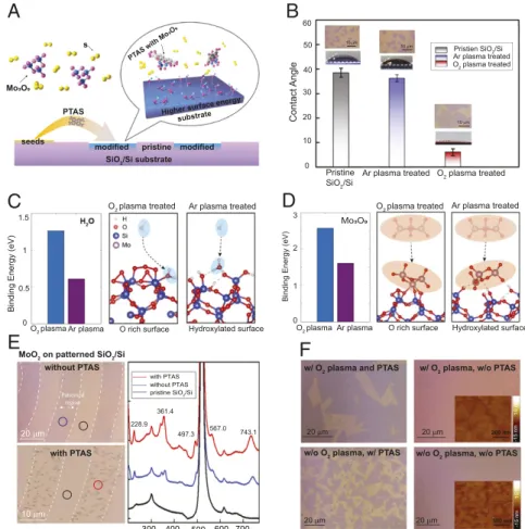
seeds PTAS
modified pristine modified Higher surface energy
substrate
Pristine SiO2/Si
Ar plasma treated O2 plasma treated
Pristien SiO2/Si
Ar plasma treated O 2 plasma treated 10 20 30 40 0 50 60 Contact Angle
B
A
D
O2 plasma Ar plasma O rich surface Hydroxylated surface
3
2
1
0
Binding Energy (eV)
O2 plasma Ar plasma O rich surface Hydroxylated surface
Binding Energy (eV)
C
1.5
1
0.5
0
MoO2 on patterned SiO2/Si
400 600 Raman Shift (cm-1) 300 500 700 228.9 361.4 567.0 743.1 497.3
w/ O2 plasma and PTAS
20 m 20 m
w/ O2 plasma, w/o PTAS
15 nm
-15 nm
F
E
with PTAS
pristine SiO2/Si
10 m 10 m
10 m
O2 plasma treated Ar plasma treated O2 plasma treated Ar plasma treated
10 m Patterned region 20 m without PTAS with PTAS without PTAS 20 m
w/o O2 plasma, w/ PTAS
20 m
w/o O2 plasma, w/o PTAS
200 nm
500 nm
15 nm
-15 nm
Fig. 2. Mechanism study for the patterned growth of monolayer MoS2 nanostructures. (A) Schematic illustration of the growth mechanism of the pat-terned growth of MoS2. (B) Comparison of contact angles for pristine, Ar plasma-treated, and O2 plasma-treated SiO2/Si substrates. (C) DFT calculation for the binding energies between H2O and SiO2/Si substrate treated by O2plasma and Ar plasma. (D) DFT calculation for the binding energies between Mo3O9 and SiO2/Si substrate treated by O2plasma and Ar plasma. (E, Upper Left) OM image of MoO2 particles preferentially deposited on patterned SiO2/ Si regions without PTAS. (E, Lower Left) OM image of MoO2 particles preferentially deposited on pat-terned SiO2/Si regions with the presence of PTAS. (E, Right) Raman spectra collected at the regions indicted by the red, blue, and black circles in the OM images in Left; several MoO2Raman peaks are la-beled in the spectra. It is shown that MoO2particles exhibit a clear preference to deposit on the pat-terned region and that the Raman peaks of MoO2 are stronger with the presence of PTAS. (F, Upper Left) OM image of monolayer MoS2flakes grown on O2plasma-treated SiO2/Si substrate with the assis-tance of PTAS. The domain size of MoS2is around 20μm. (F, Upper Right) OM image of small MoS2 flakes grown on O2plasma-treated SiO2/Si substrate without PTAS. (Inset) AFM images of MoS2 small flakes with domain size around 300 nm. (F, Lower Left) OM image of monolayer MoS2flakes grown on pristine SiO2/Si substrate with the assistance of PTAS. The domain size of MoS2 is around 8–10 μm. (F, Lower Right) OM image of small MoS2flakes grown on pristine SiO2/Si substrate without PTAS seed. (In-set) AFM images of MoS2small flakes with domain size around 200 nm, indicating the poor quality of MoS2growth.
ENGINEER
epitaxial layers and the substrates (28). Therefore, increasing the surface energy on selective areas of the substrate favors patterned monolayer growth over the growth of multilayer particles. As shown in Fig. 2A, after patterning and O2plasma treatment, the SiO2/Si
substrate was composed of modified regions and pristine regions. We compared the contact angles for each type of surface in Fig. 2B. The contact angle of pristine SiO2/Si substrate is around 38.48°, while it
drops rapidly to 6.04° after O2plasma treating for 10 min, similar to
observations in previous reports (19). To compare the change in the physical surface due to O2plasma treatment, we also measured the
contact angle of the surface treated by Ar plasma for the same du-ration (which gives similar surface roughness) (SI Appendix, Fig. S8). However, the Ar plasma-treated substrate shows a contact angle of about 36.22°, similar to that of the pristine SiO2/Si. Thus, physical
roughness is not the main contribution to the surface energy change. To understand the difference in surface energies induced by different treatments, we conducted density functional theory (DFT) calculations. In our model, Ar plasma etching increases the number of dangling bonds on the surface of SiO2/Si
sub-strate, which serve as active sites to dissociate H2O molecules in
ambient environment, resulting in a hydroxylated surface (ter-minated by–OH group) (SI Appendix, Fig. S9). However, in the case of O2plasma, the oxygen bonds on the unsaturated surface
site and yields an oxygen-rich surface. DFT calculations show that the binding energy of water with the oxygen-rich surface is over two times that of the Ar plasma-treated surface (Fig. 2C), consistent with the contact angle measurement in Fig. 2B. When considering the binding energy with Mo3O9[the intermediate of
MoO3−xduring the MoS2growth (29)], the oxygen-rich surface
has∼1-eV higher binding energy than that of the hydroxylated surface (Fig. 2D). Combining the growth result (SI Appendix, Fig. S10) with DFT calculations, it is shown that the O2plasma-modified
substrates have better wettability and higher binding energy to Mo3O9, which is beneficial for the monolayer growth of MoS2. We
experimentally verify this via results shown in Fig. 2E. On only supplying MoO3powder during the growth, Mo-containing species
[MoO2as confirmed by Raman spectroscopy (30)] clearly preferred
the O2 plasma-treated regions over the nontreated regions. By
adding PTAS, which is a hydrophilic salt and has preference for the patterned regions (23), Mo-based compounds may have higher adsorption within the patterned regions (as given by a stronger Raman signature after PTAS was added). Here, the presence of PTAS may increase the strength of surface adhesion between MoS2
and SiO2/Si, leading to the monolayer growth of MoS2. Based on
the different growth results in Fig. 2F, which show obvious growth enhancement under O2plasma and PTAS, we conclude that the
combination of O2 plasma treatment and PTAS exhibits a
syner-getic effect that promotes the optimized MoS2growth.
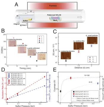
For the MoS2growth to distinguish the difference between the
untreated and treated surfaces, we noted that the entrance timing of sulfur and its amount are critical, both of which will affect the concentration (or partial pressure) of sulfur in the gaseous phase. According to the Mo–O–S phase diagram (31), MoO3undergoes a two-step reaction in the chemical vapor
de-position (CVD) growth of MoS2(32):
MoO3ðsÞ + x=2SðgÞ → MoO3−xðgÞ + x=2SO2ðgÞ. [1]
Next, MoO3−x(g) has two possible reaction paths:
MoO3−xðgÞ + ð7 − xÞ=2SðgÞ → MoS2ðsÞ + ð3 − xÞ=2SO2ðgÞ [2.1]
MoO3−xðgÞ + ð1 − xÞ=2SðgÞ → MoO2ðsÞ + ð1 − xÞ=2SO2ðgÞ.
[2.2] Higher [S]/[Mo] ratio (here, [S] and [Mo] indicate the con-centrations or partial pressures of S and Mo species) promotes
the reaction in path [2.1], while lower [S]/[Mo] ratio tends to form MoO2as path [2.2]. To investigate the role of sulfur, we
laid several patterned substrates as shown inSI Appendix, Fig. S11A(23). Presumably, the sulfur concentration decreases along the substrate as the distance away from the sulfur source in-creases, and the quality of the MoS2patterns in different regions
of SiO2/Si reflects the influence of sulfur concentration on the
patterned growth. Instead of producing spatially distinguished MoS2patterns, higher sulfur concentration creates a continuous
MoS2 film across the entire surface (SI Appendix, Fig. S11B)
(which means that there is no selective patterning by the sub-strate), while lower sulfur concentration produces discontinuous MoS2flakes (SI Appendix, Fig. S11E). Only under an appropriate
concentration, we can produce patterned monolayer MoS2(SI
Appendix, Fig. S11D). Therefore, we designed an improved CVD setup to control sulfur concentration during the growth. As shown in Fig. 3A, a small quartz tube is used to carry the sul-fur boat, and a set of magnets is used to move the position of the sulfur boat. The sulfur powder is initially kept outside of the heating zone, and it is moved inside the heating zone during the ramping period when the MoO3 precursor reaches a suitable
temperature (SI Appendix, Fig. S12) (it takes 15 min for the center of the furnace to reach the growth temperature). We first found that the entrance timing of sulfur impacts the ratio of sulfur partial pressure to Mo partial pressure ([S]/[Mo]) due to the temperature difference at different entrance times (SI Ap-pendix, Fig. S13 and Table S1). As shown in Fig. 3B, the [S]/[Mo] ratio has a negative correlation with the entrance timing of
1 1.5 2 Distance (d) (cm) 100 2 m d2: continus film 2 m d3: small particles 2 m d1: coalescing domains [S] (atm. 10 -6) 5 m t3:partly sulfurized t4:un-sulfurized [S]/[Mo] 10¹ 10² 10³ 104 d1 d2 d3
C
B
13 14 15 Timing (min) 12 0 50 100 150 200 t1 t2 t3 t4 t1:coalescing domains t2:continus film 5 mA
MoO3Patterned SiO2/Si
magnet Sulfur d @ time t Furnace Ar 0 0.1 0.2 0.3
Sulfur Pressure (torr)
3 2 1 0 Nucleation Rate (N / m 2) 0 0.1 0.2 0.3
Sulfur Pressure (torr)
1 0.5 0 Coverage (Θ) 4 5
Fitting of 3D growth rate
Fitting of nucleation rate
30 20 10 0 40 3D Growth Rate (*10 -3 m 3 /min )
D
Fitting in Frank-Van der Merwe mode Fitting in Volmer-Weber mode
K=190 K=9
E
11.4 5.7 0.0 2D Growth Rate m 2 /min 10 m 1 1 1 1 1 1 1 1 1000000000mmm 5 m 5 mFig. 3. The control of sulfur precursor during the patterned growth of monolayer MoS2nanostructures. (A) Schematic illustration of the modified CVD setup and the controlled process to synthesize patterned MoS2 nano-structures. (B) The relationship between the entrance time of the sulfur precursor and the corresponding [S]/[Mo] ratio during the growth. (Insets) OM images of different growth results according to different entrance times of sulfur. (C) The relationship between the locations of the sulfur precursor (d) and the corresponding vapor pressures of sulfur. (Insets) AFM images of MoS2patterns grown as a result of different precursor locations. (D) The dependence of nucleation rate as the function of partial pressure of sulfur precursor (left y axis); the dependence of 3D growth rate as the function of partial pressure of sulfur precursor (right y axis). (E) The dependence of surface coverage as the function of partial pressure of sulfur precursor (left y axis); the dependence of 2D growth rate as the function of partial pressure of the sulfur precursor (right y axis).
sulfur, which essentially dominates the degree of the sulfuriza-tion in the process. When sulfur is introduced relatively early (as shown in Fig. 3B) (at t1or t2; before 14 min), the [S]/[Mo] is high
enough to fully sulfurize MoO3 into MoS2. Nevertheless, to
make continuous MoS2 patterns, sufficient supply of
molybde-num is also required (entering at t2) compared with the lower
supply of molybdenum at t1. However, when sulfur enters at t3,
the [S]/[Mo] ratio decreases rapidly, resulting in only a part of MoO3turning into MoS2. If sulfur enters at t4or later, only black
MoO2particles are obtained on the substrate. Although MoO2
can also be sulfurized into MoS2(33), the temperature needed
(650 °C to 850 °C) is much higher than that in our growth. Ad-ditionally, the position where the sulfur boat is introduced (corresponding to the distance d in Fig. 3C and as illustrated in Fig. 3A) is another important factor of sulfur pressure, which therefore, determines the nucleation rate and growth rate of MoS2. According to the temperature variation at different
po-sitions (i.e., different d values) (SI Appendix, Fig. S14), we semiquantitatively calculated the nucleation rate and the growth rate of the patterned growth of monolayer MoS2(SI Appendix,
Table S2). In Fig. 3C, the [S] at d1is insufficient, leading to both
low nucleation rate (Fig. 3D) and growth rate (Fig. 3E). While excess [S] at d3will increase the nucleation rate of MoS2
dra-matically, it also accelerates the MoS2nuclei growth rate in the
vertical direction (corresponding to the 3D growth rate in Fig. 3D), which is significantly faster than that in the lateral direction (corresponding to 2D growth rate in Fig. 3E), leading to the formation of multilayer MoS2 particles. If the sulfur partial
pressure is kept at an appropriate value (located at d2), we could
achieve medium nucleation rate and optimal growth rate in the lateral direction and obtain monolayer MoS2patterns.
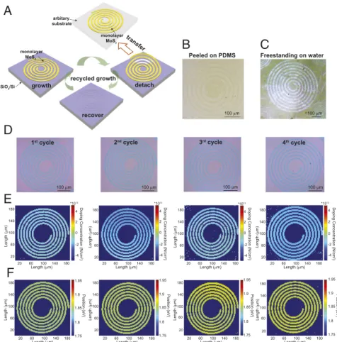
As previously mentioned, electronic applications require pat-terned materials for device fabrication and integration. Never-theless, previous methods to produce patterned 2D materials are limited by the single use of patterned substrates or etched ma-terials. Therefore, developing a master–replica type of repeated growth of patterned TMD materials is highly attractive for 2D material device fabrication. Here, we have found that the pre-patterned substrate can be repeatedly used through the non-invasive transfer of monolayer MoS2patterns. As shown in Fig.
4A, due to the weak interaction between the monolayer MoS2
and the SiO2/Si substrate, monolayer MoS2patterns can be easily
detached (with preserved structural integrity) from the substrate by directly peeling with a polydimethylsiloxane (PDMS) stamp via dry transfer (Fig. 4B) or delaminating by water via wet transfer (Fig. 4C andSI Appendix, Figs. S15 and S16). Since the separation process is performed without any intermediate sup-porting layer or etchant, the released substrate with original patterns is recovered, which makes it possible for the next cycle of patterned growth. In our study, it was found that the patterned substrate can be reused at least four times without seeing signs of wear, and the quality of monolayer MoS2patterns is well preserved.
Fig. 4D shows the OM images of MoS2spiral patterns grown from
four “growth–detach” cycles on the same SiO2/Si substrate after
water delamination. It was found that the shape of the MoS2spiral
in each cycle was well reserved and that the reflectance contrast was
100 m 1st cycle 100 m 2nd cycle 100 m 3rd cycle 100 m 4th cycle
E
100 180 0 2 60 140 Length ( m) 180 20 60 100 140 Length ( m) 4 2 0 -2 -4 Doping Concentration (N/cm 2 ) *1013 180 20 60 100 140 Length ( m) 100 180 0 2 60 140 Length ( m) 4 2 0 -2 -4 Doping Concentration (N/cm 2 ) *1013 detach recover growth SiO2/Si monolayer MoS2 recycled growth monolayer MoS2 arbitary substrateA
100 m 100 m Freestanding on water Peeled on PDMSC
B
D
F
4 2 0 -2 -4 Doping Concentration (N/cm 2 ) *1013 100 180 0 2 60 140 Length ( m) 180 20 60 100 140 Length ( m) 4 2 0 -2 -4 Doping Concentration (N/cm 2 ) *1013 100 180 0 2 60 140 Length ( m) 180 20 60 100 140 Length ( m) 100 180 0 2 60 140 Length ( m) 180 20 60 100 140 Length ( m) 1.95 1.9 1.85 1.8 1.75 Position (eV) 100 180 0 2 60 140 Length ( m) 180 20 60 100 140 Length ( m) 1.95 1.9 1.85 1.8 1.75 Position (eV) 180 20 60 100 140 Length ( m) 100 180 0 2 60 140 Length ( m) 1.95 1.9 1.85 1.8 1.75 Position (eV) 1.95 1.9 1.85 1.8 1.75 Position (eV) 100 180 0 2 60 140 Length ( m) 180 20 60 100 140 Length ( m) transferFig. 4. Repeated growth of patterned monolayer MoS2nanostructures using the same template. (A) Schematic illustration of repeated growth procedures for directly grown MoS2patterns. (B) OM image of monolayer MoS2patterns peeled on PDMS. (C) OM image of monolayer MoS2structures freestanding on water without any additional support. (D) OM images of the monolayer MoS2spiral pattern after the first, second, third, and fourth growth cycles. (E) The carrier concentration mappings (via Raman) of the monolayer MoS2spiral after the first, second, third, and fourth growth cycles as given by D. (F) The photoluminescence position mappings (via PL spectrum) of the monolayer MoS2spiral after the first, second, third, and fourth growth cycles as given by D.
ENGINEER
uniform under the same illumination. The OM images of SiO2/Si
substrates before growth and after delamination (SI Appendix, Fig. S17) show that premade patterns on SiO2/Si substrate are retained
after this simple and clean transfer without visible damage and contamination. From our calculation, the O2 plasma-treated
sub-strates have lower binding energy with hydrocarbon species (the common contaminate in air) (SI Appendix, Fig. S18), which suggests a“contamination-resilient” feature of O-rich surfaces. This could be verified by our observation that the patterned substrates kept for several weeks are still as effective to patterned growth as freshly made. To evaluate the quality of the MoS2patterns grown by the
recycled growth, we extracted strain (SI Appendix, Fig. S19) and carrier concentration maps (Fig. 4E) from the spatially resolved Raman analysis (34, 35) on the MoS2spirals grown each time using
the same SiO2/Si template. The strain and carrier concentration
maps show a relatively small variation, indicating good consistency in the quality of MoS2patterns for different cycles. Moreover, the
PL spectrum on monolayer MoS2from each cycle has few changes
on the emission energy and FWHM (SI Appendix, Fig. S20). The photoluminescence position mappings (Fig. 4F) extracted from the PL spectrum analysis also demonstrate the preserved qualities. After delamination, these MoS2patterns floating on a water surface
can be easily picked up onto arbitrary substrates, such as trans-parent quartz (SI Appendix, Fig. S21A) and flexible mica (SI Appendix, Fig. S21B), allowing for more efficient integration of complicated 2D device structures.
The key for repeated utilization of the same mask relies on the successful delamination (hence, on the quality of the monolayer MoS2 patterns). If MoS2 particles are grown, the patterns are
difficult to delaminate by water, which will damage the surface integrity and reduce the lifetime of the master template. With well-controlled growth, successful transfer, and posttreated cleaning, it is anticipated that these prepatterned templates can be used many times. This additive manufacturing method paves
the way for broad applications of 2D TMD nanostructures in modern electronics and optoelectronics with much simpler fab-rication, lower cost, and higher efficiency.
Methods
To obtain patterned substrates for MoS2growth, photolithography and O2 plasma treatment steps were first carried out as explained above. After re-moving the photoresist on the patterned SiO2/Si wafer, the substrate was preannealed at 350 °C for 2 h with 300 standard cubic centimeters per minute (sccm) Ar and 100 sccm H2gases. Then, a piece of the patterned substrate was suspended between two SiO2/Si substrates with predeposited PTAS (via solution dropping). All of these substrates were placed face down on a crucible containing MoO3precursor in a 1-inch quartz tube. This cru-cible was placed in the middle of the heating zone with another smaller tube containing the sulfur crucible upstream close to the cold end of the quartz tube. Before heating, the whole CVD system was purged with 1,000 sccm Ar (99.999% purity) for 3 min. Then, 20 sccm Ar was introduced into the system as a carrier gas. The growth system was heated to 625 °C for 15 min. At around 13 min, the sulfur crucible was pushed into the system by a magnet (as shown in Fig. 3A) at a distance of∼1.5 cm from the left edge of the furnace. The MoS2growth was carried out around 620 °C to 630 °C for 3 min under atmospheric pressure. The growth system was finally cooled down to room temperature quickly by opening the furnace and cooling using a fan.
ACKNOWLEDGMENTS. We acknowledge support from Air Force Office of Scientific Research Multidisciplinary University Research Initiative-Foldable and Adaptive Two-Dimensional Electronics Program Grant FA9550-15-1-0514, the Center for Energy Efficient Electronics Science through NSF Grant 0939514, the US Army Research Office through Massachusetts Institute of Technology Institute for Soldier Nanotechnologies Grant 023574, the Center for Integrated Quantum Materials, Science and Technology Center through NSF Grant DMR-1231319 (to Q.J. and Y.L.), and King Abdullah University of Science and Technology Contract OSR-2015-CRG4-2634. Y.H. and D.A.M. ac-knowledge the Cornell Center for Materials Research for funding through NSF Materials Research Science and Engineering Centers Program DMR-17198751. X.L. acknowledges the support of Boston University.
1. Radisavljevic B, Kis A (2013) Mobility engineering and a metal-insulator transition in monolayer MoS2. Nat Mater 12:815–820.
2. Bertolazzi S, Brivio J, Kis A (2011) Stretching and breaking of ultrathin MoS2. ACS
Nano 5:9703–9709.
3. Mak KF, McGill KL, Park J, McEuen PL (2014) Valleytronics. The valley hall effect in MoS2transistors. Science 344:1489–1492.
4. Wu W, et al. (2014) Piezoelectricity of single-atomic-layer MoS2for energy conversion
and piezotronics. Nature 514:470–474.
5. Feng Q, et al. (2014) Semiconductors: Growth of large-area 2D MoS2(1-x)Se2x
semi-conductor alloys (Adv. Mater. 17/2014). Adv Mater 26:2763.
6. Radisavljevic B, Radenovic A, Brivio J, Giacometti V, Kis A (2011) Single-layer MoS2
transistors. Nat Nanotechnol 6:147–150.
7. Wang QH, Kalantar-Zadeh K, Kis A, Coleman JN, Strano MS (2012) Electronics and optoelectronics of two-dimensional transition metal dichalcogenides. Nat Nanotechnol 7:699–712.
8. Zheng W, et al. (2015) Patterning two-dimensional chalcogenide crystals of Bi2Se3and
In2Se3and efficient photodetectors. Nat Commun 6:6972.
9. Yu Q, et al. (2011) Control and characterization of individual grains and grain boundaries in graphene grown by chemical vapour deposition. Nat Mater 10: 443–449.
10. Zhou H, et al. (2013) Thickness-dependent patterning of MoS2sheets with
well-oriented triangular pits by heating in air. Nano Res 6:703–711.
11. Mahjouri-Samani M, et al. (2015) Patterned arrays of lateral heterojunctions within monolayer two-dimensional semiconductors. Nat Commun 6:7749.
12. Xue Y, et al. (2016) Scalable production of a few-layer MoS2/WS2vertical
hetero-junction array and its application for photodetectors. ACS Nano 10:573–580. 13. Park W, et al. (2014) Photoelectron spectroscopic imaging and device applications of
large-area patternable single-layer MoS2synthesized by chemical vapor deposition.
ACS Nano 8:4961–4968.
14. Cao L, et al. (2013) Direct laser-patterned micro-supercapacitors from paintable MoS2
films. Small 9:2905–2910.
15. Kelly AG, et al. (2017) All-printed thin-film transistors from networks of liquid-exfoliated nanosheets. Science 356:69–73.
16. Han GH, et al. (2015) Seeded growth of highly crystalline molybdenum disulphide monolayers at controlled locations. Nat Commun 6:6128.
17. Song I, et al. (2014) Patternable large-scale molybdenium disulfide atomic layers grown by gold-assisted chemical vapor deposition. Angew Chem Int Ed Engl 53: 1266–1269.
18. Kim H-J, Kim H, Yang S, Kwon J-Y (2017) Grains in selectively grown MoS thin films. Small 13:1702256.
19. Chen X, et al. (2016) Lithography-free plasma-induced patterned growth of MoS2and
its heterojunction with graphene. Nanoscale 8:15181–15188.
20. Shyu TC, et al. (2015) A kirigami approach to engineering elasticity in nanocomposites through patterned defects. Nat Mater 14:785–789.
21. Lamoureux A, Lee K, Shlian M, Forrest SR, Shtein M (2015) Dynamic kirigami struc-tures for integrated solar tracking. Nat Commun 6:8092.
22. Blees MK, et al. (2015) Graphene kirigami. Nature 524:204–207.
23. Ling X, et al. (2014) Role of the seeding promoter in MoS2growth by chemical vapor
deposition. Nano Lett 14:464–472.
24. Ling X, et al. (2016) Parallel stitching of 2D materials. Adv Mater 28:2322–2329. 25. van der Zande AM, et al. (2013) Grains and grain boundaries in highly crystalline
monolayer molybdenum disulphide. Nat Mater 12:554–561.
26. Kang K, et al. (2015) High-mobility three-atom-thick semiconducting films with wafer-scale homogeneity. Nature 520:656–660.
27. English CD, Shine G, Dorgan VE, Saraswat KC, Pop E (2016) Improved contacts to MoS2
transistors by ultra-high vacuum metal deposition. Nano Lett 16:3824–3830. 28. ten Wolde PR, Frenkel D (1997) Enhancement of protein crystal nucleation by critical
density fluctuations. Science 277:1975–1978.
29. Burns RP, DeMaria G, Drowart J, Grimley RT (1960) Mass spectrometric investigation of the sublimation of molybdenum dioxide. J Chem Phys 32:1363–1366.
30. Kumari L, et al. (2007) X-ray diffraction and Raman scattering studies on large-area array and nanobranched structure of 1D MoO2 nanorods. Nanotechnology 18:
115717.
31. Li H, Li Y, Aljarb A, Shi Y, Li L-J (2018) Epitaxial growth of two-dimensional layered transition-metal dichalcogenides: Growth mechanism, controllability, and scalability. Chem Rev 118:6134–6150.
32. Chhowalla M, et al. (2013) The chemistry of two-dimensional layered transition metal dichalcogenide nanosheets. Nat Chem 5:263–275.
33. Wang X, Feng H, Wu Y, Jiao L (2013) Controlled synthesis of highly crystalline MoS2
flakes by chemical vapor deposition. J Am Chem Soc 135:5304–5307.
34. Michail A, Delikoukos N, Parthenios J, Galiotis C, Papagelis K (2016) Optical detection of strain and doping inhomogeneities in single layer MoS2. Appl Phys Lett 108:
173102.
35. Chae WH, Cain JD, Hanson ED, Murthy AA, Dravid VP (2017) Substrate-induced strain and charge doping in CVD-grown monolayer MoS2. Appl Phys Lett 111:143106.