Calibration of Sampling Clock Skew in
High-Speed, High-Resolution Time-Interleaved
ADCs.
by
Daniel Kumar
Submitted to the Department of Electrical Engineering and Computer
Science
in partial fulfillment of the requirements for the degree of
Doctor of Philosopy in Electrical Engineering and Computer Science
at the
MASSACHUSETTS INSTITUTE OF TECHNOLOGY
June
2015
Massachusetts Institute of Technology 2015.
A
ATn
All rights reserved.
__
J0.
Signature redacted
Author ...
...
Department of Electrical Engineering and Computer Science
March 27, 2015
Certified by...
Signature redacted
Hae-Seung Lee
Advanced Television and Signal Processing Professor of Electrical
Engineering
Thesis Supervisor
Accepted by ...
Signature redacted
. . . .
' / ) //
Leslie A. Kolodziejski
MASSACHUSETTS INSTITUTE OF TECHNOLOLGY
JUL 0
7
2015
Calibration of Sampling Clock Skew in High-Speed,
High-Resolution Time-Interleaved ADCs.
by
Daniel Kumar
Submitted to the Department of Electrical Engineering and Computer Science on March 27, 2015, in partial fulfillment of the
requirements for the degree of
Doctor of Philosopy in Electrical Engineering and Computer Science
Abstract
There is an ever-increasing demand for high-resolution and high-resolution ADCs. In order to raise the sampling rates of ADCs in a power efficient manner, time-interleaving is an essential technique, whereby N ADC channels, each operating at a sampling frequency of
f
8, are used to achieve an effective conversion rate of N -f,.
While time-interleaving enables higher conversion rates in a given technology, mismatch issues such as gain, offset, and sampling clock skew between channels de-grade the overall time-interleaved ADC performance. Of these issues, sampling clock skew between channels is the biggest problem in high-speed and high-resolution, time-interleaved ADCs as errors due to sampling clock skew become more severe for higher input frequencies. There are a few sources of sampling clock skew between channels. Mismatches in the sampling clock path and logic delays are the most obvious ones. Input signal routing mismatch and RC mismatch of the input sampling circuits also cause sampling clock skew.
In this thesis, we developed two new methods to mitigate the effects of sampling clock skew in time-interleaved ADCs. The first is the rapid consecutive sampling method, whereby each interleaved channel is implemented using two sub-channel ADCs. Two consecutive samples of the input are taken with a short time delay between them. This allows for a straight-forward linear interpolation between the consecutive samples in order to recover the de-skewed sample. The second method entails introducing a programmable delay in the input signal path, instead of delaying the sampling clock, in order to calibrate out sampling clock skew. The design and implementation of a proof-of-concept, time-interleaved ADC that implements the input signal delay method is detailed. Finally, measurement results to show the efficacy of the proposed method in mitigating the effects of sampling clock skew is also presented.
Thesis Supervisor: Hae-Seung Lee
Acknowledgments
I would like to first thank my advisor, Professor Hae-Seung Lee. It has been a terrific
opportunity to work with him. His technical guidance has been stellar and I have
learned much about circuit design from him. I have always been amazed by the breadth and depth of his knowledge. However, what inspires me the most is his
unwavering support and ability to see the best way forward when problems seem insurmountable, both with regards to research and life in general. For that, I will be
ever grateful.
I would also like to thank the members of my thesis committee, Professor Anantha
Chandrakasan and Professor Charles Sodini. I have gained a lot from their teaching, advice, feedback, and support over the years. I would also like to thank Professor
Ayman Shabra for his valuable technical feedback.
Another highlight of graduate school was the people I had a chance to work
with. Bruno DoValle, Kohei Onizuka, Eric Winokur, Sabino Pietrangelo, Do Yeon Yoon, Xi Yang, SungWon Chung, Mariana Markova, Albert Chang, Sunghyuk Lee, Kailiang Chen, Hyun Boo, Grant Anderson, Joohyun Seo, Harneet Khurana, and
Maggie Delano have been great colleagues. Beyond the doors of 38-265, my thanks goes to Lorenzo Turicchia, Wei Li, Woradorn Wattanapanitch, Scott Arfin, Arun
Paidimarri, Soumyajit Mandal, Micah O'Halloran, and Shirin Farrahi too. Their
generosity in time and thoughtful advice (both technical and otherwise) has been humbling. Graduate school is a team sport, and I'm grateful to have had them on
my team!
My time at MIT would also have been much less enjoyable if not for the close
friends that have continually brought joy and companionship into my life. Omair
Saadat, Siddharth Bhardwaj, Himanshu Dhamankar, Somani Patnaik, Johann John, Edward Boenig, Margo Liptsin, Victor Li, Paul Wilson, and Marc Biel. I cherish your friendship.
Finally, it would be remiss of me if I did not thank my family. My parents and siblings have cheered me on through the highlights and supported me through the
tough times. For that, I am eternally grateful. To Jaisree, you're probably my best
Contents
1 Introduction 23
1.1 Time-Interleaved ADCs. ... 25
1.2 Thesis Organization . . . . 29
2 Operation of Time-Interleaved ADCs 31 2.1 Single Channel Sampling . . . . 32
2.1.1 Single Channel Sampling in Time-Domain . . . . 33
2.1.2 Single Channel Sampling in Frequency-Domain . . . . 34
2.2 Time Interleaved Sampling . . . . 35
2.2.1 Multi-Channel, Time-Interleaved Sampling in Time Domain . 36 2.2.2 Multi-Channel, Time-Interleaved Sampling in Frequency-Domain 38 2.3 The Effect of Channel Errors on the Performance of Time-Interleaved ADC System s . . . . 40
2.3.1 Offset Mismatch Between Channels . . . . 42
2.3.2 Gain Mismatch Between Channels . . . . 44
2.3.3 Sampling Clock Skew Between Channels . . . . 49
2.4 Comparison of Channel Mismatches . . . . 54
3 Sampling Clock Skew Errors in Time-Interleaved ADCs 57 3.1 Major Sources of Sampling Clock Skew . . . . 57
3.1.1 Skew Due to Transistor Variations . . . . 58
3.1.2 Skew Due to Variations in Clock and Signal Routing . . . . . 61
3.2.1 Two-Rank Track-and-Hold . . . . 63
3.2.2 Channel Randomization . . . . 65
3.3 Calibration and Correction Methods to Mitigate Effects of Sampling Clock Skew . . . . 65
3.3.1 Sampling Clock Skew Detection . . . . 67
3.3.2 Calibration and Correction of Sampling Clock Skew . . . . 73
3.4 Sum m ary . . . . 80
4 Proposed Sampling Clock Skew Calibration Methods 81 4.1 Rapid Consecutive Sampling (RCS) Method . . . . 82
4.1.1 Bound on Delay Between Samples . . . . 85
4.1.2 Behavioral Simulation Results of the RCS Technique . . . . . 87
4.1.3 Challenges in Implementing the RCS Technique . . . . 88
4.2 Input Signal Delay Control Method . . . . 91
4.2.1 Fine Input Signal Delay Control Using Low-Pass Filters . . . . 93
4.2.2 Behavioral Simulation Results of the Input Signal Delay Con-trol Technique . . . . 96
4.2.3 Input Sampling Bandwidth Requirements . . . . 98
4.2.4 Effect of Residual Gain Mismatch . . . . 100
4.3 Sum m ary . . . . 102
5 Prototype Time-Interleaved SAR ADC Circuit Design 105 5.1 Interleaved Channel Converter Architecture . . . . 106
5.2 SAR ADC Block Diagram . . . . 108
5.3 DAC Design . . . . 109
5.4 Input Sampling Network . . . .111
5.4.1 Bottom Plate Sampling . . . .111
5.4.2 Bootstrapped Sampling Switch . . . . 113
5.4.3 Input Signal Delay Control . . . . 116
5.5 Latch Comparator . . . . 118
5.7 Multi-Phase Clock Generator . . . . 128
5.8 Off-Chip References . . . . 131
5.9 Layout . . . . 133
5.10 Summary . . . . 133
6 Test Setup and Measurement Results 137 6.1 Test Setup . . . . 137
6.1.1 Prototype Chip . . . . 137
6.1.2 Printed Circuit Board (PCB) . . . . 137
6.1.3 Measurement Setup . . . . 139 6.2 Measurement Results . . . . 139 6.2.1 Static Performance . . . . 145 6.3 Performance Summary . . . . 146 6.4 Summary . . . . 148 7 Conclusions 151 7.1 Summary . . . . 151 7.2 Future Work. . . . . 153
List of Figures
1-1 Block diagram of a typical signal-chain for electronic systems. .... 24 1-2 Plot of power consumption vs. input signal Nyquist bandwidth. The
curved line shows the expected power growth if a single channel ADC
is used to achieve increasing bandwidths. The linear line shows the expected power consumption of an ideal time-interleaved ADC with
increasing bandwidths (with power of overhead circuitry to implement time-interleaving excluded). . . . . 25 1-3 Block diagram of a time-interleaved ADC. . . . . 27
1-4 Plot of Schreier FOM vs Nyquist sampling frequencies for all ADC
papers presented at ISSCC and VLSI from 1997-2014. . . . . 28
2-1 Block diagram of a typical Nyquist-rate ADC. . . . . 32
2-2 Block diagram of a sampling system. . . . . 33 2-3 Time-domain representation of a continuous signal, x(t), sampled using
a delta train function, d(t) . . . . . 34 2-4 Frequency-domain representation of a continuous signal, X(jw),
sam-pled using a delta train function, D(jw). . . . . 35 2-5 Block diagram of a N-way time-interleaved sampler. The delta trains,
di(t), are used to sample the i-th channel and are delayed by T/N from each other. . . . . 36
2-6 Time-domain representation of a 4-way time-interleaved system. The sampling period of each delta train is T, but the delta train for each channel is shifted by T/N from each other. The sampled output, x5(t) appears to be sampled with a sampling period of T/4. . . . . 38
2-7 Frequency-domain representation of a 2-way time-interleaved system. While the spectrum of each of the channels show aliasing in the
fre-quency spectrum, the summed output does not suffer from aliasing. The images centered at 7r, 37r,... from the odd and even channels
(denoted using a shaded image) cancel each other out, leaving the
re-sulting spectrum free of aliasing artifacts. . . . . 41
2-8 Block diagram of a time-interleaved ADC with offset mismatch between channels modeled as an additive voltage source, V,,oi, at the input of
the i-th channel. . . . . 43
2-9 Behavioral simulation results of the time domain error due to offset mismatches between channels. The plot in panel (a) shows a 12-bit
output of a 4-way time-interleaved ADC with offset mismatch between channels. The graph in panel (b) shows the error in LSBs of the time-interleaved system with offset mismatch from the ideal, expected
out-put code when no offset mismatch between channels is present. ... 43
2-10 A frequency spectrum of the output of a behavioral simulation of a 4-way time-interleaved ADC with offset mismatches between channels.
The spurs at f,/2 and f,/4 are due to the offset mismatches between channels in the time interleaved ADC. . . . . 45
2-11 Block diagram of a time-interleaved ADC with gain mismatch between channels modeled as an gain block with gains, Gaj before the input of
2-12 Behavioral simulation results of the time domain error due to gain
mis-matches between channels. The plot in panel (a) shows a 12b output of
a 4-way time-interleaved ADC with gain mismatch between channels. The graph in panel (b) shows the error in LSBs of the time-interleaved
system with offset mismatch from the ideal, expected output code. . . 47
2-13 A frequency spectrum of the output of a behavioral simulation of a
4-way time-interleaved ADC with gain mismatches between channels. The pair of spurs spaced by
+fi,
aroundf,/4
and f,/2 are due to the gain mismatches between the channels in the time interleaved ADC. . 48 2-14 Block diagram of a time-interleaved ADC with sampling clock skewbetween channels modeled as a time delay Ati added to the clock signal
of the i-th channel. . . . . 49
2-15 Behavioral simulation results of the time domain error due to sampling
clock skew between channels. The plot in panel (a) shows a 12-bit
output of a 4-way time-interleaved ADC with sampling clock skew between channels. The graph in panel (b) shows the error in LSBs
between output of the time-interleaved system with sampling clock
skew and an the expected output code for an ideal, skew-free, time-interleaved system . . . . 50 2-16 The same sampling clock skew results in a voltage error proportional
to the gradient of the input error during the sampling instant. .... 51 2-17 A frequency spectrum of the output of a behavioral simulation of a
4-way time-interleaved ADC with sampling clock skew between channels. The pair of spurs spaced by
fi,
aroundf,/4
and f,/2 are due to the sampling clock skew between channels in the time interleaved ADC. . 53 2-18 SNDR vs input signal frequency for a 4-way, 12-bit, time-interleaved3-1 Sampling clock for a time-interleaved ADC. CLKFs is the full-speed clock. The i-th interleaved channel is sampled on the falling edge of
C ki. . . . . 58
3-2 Circuit schematic of a multi-phase clock generator. The output of each
AND gate is buffered to drive the clock routing interconnects to the
individual channels. . . . . 59 3-3 Circuit schematic of the input sampling network during the track phase. 60 3-4 Possible routing schemes for the input signal and clock in a
time-interleaved ADC: (a) input signal and clocks are routed linearly, (b) input signal and clocks are routed in a H-tree fashion. . . . . 62 3-5 Time-interleaved ADC with a global T/H that samples the input
sig-nal. The T/H within each interleaved channel re-samples the output
of the global T/H. . . . . 64
3-6 Time-interleaved ADC with channel randomization to mitigate
sam-pling clock skew. P-channels are used to implement an N-way
time-interleaved ADC, where P/gtN . . . . 66 3-7 Sampling-clock skew calibration or correction process. . . . . 67 3-8 Sampling clock skew estimation using out-of-energy calculation for
bandlimited input signals. . . . . 69 3-9 Zero-crossing for a 2-way interleaved ADC without skew (a), and with
tim ing skew (b). . . . . 70 3-10 Estimation of sampling clock skew between the ADC under test and
the calibration (CAL) ADC. x(t) is the input signal and # and 0,aI
are the clocks for the ADC channel under test and the CAL ADC
respectively. Source:[21] . . . . 71 3-11 Popular circuit implementations of variable delay lines. In (a), a
vari-able load capacitance is used to control the delay of Clkd, while in (b)
3-12 Jitter addition from variable delay lines. When the clock edge is slowed
down, it becomes more susceptible to noise near threshold of the
re-timing inverter, leading to increased jitter in the ouput clock . . . . . 76
3-13 The effect of increasing slew rates and inverter noise on tthresh.. ... 77
3-14 Sampling clock skew correction using a fractional delay filter, H(z) . 78
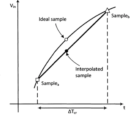
4-1 For small sampling clock skews, linear extrapolation can be used to estimate a skew-free sample. . . . . 82
4-2 Using linear interpolation to estimate the skew free sample using two samples of the input signal Samplea, and Sampleb of the input taken
before and after the ideal sampling instant. . . . . 83
4-3 Block diagram of a time-interleaved ADC with RCS. . . . . 84
4-4 Timing diagram of a time-interleaved ADC with RCS. . . . . 84
4-5 Error between the estimate of the input signal and the actual value when linear interpolation applied using two samples separated by AT,.
for various input signal frequencies. . . . . 86
4-6 Output spectrum of a behavioral simulation for a four-way time inter-leaved ADC with sampling clock skew. In (a), the output spectrum of
the uncalibrated ADC is shown, and in (b) the output spectrum after calibration for an ADC utilizing the RCS technique is shown . . . . . 87
4-7 Input disturbance after sub-channel sampling for the i-th channel in
time-interleaved ADC with RCS. . . . . 88
4-9 Controlling the delay of the input signal as a method to calibrate out sampling clock skew. In (a), the usual method for sampling clock skew
calibration is presented. Here the sampling clock edge is shifted such that the effects of sampling clock skew is removed. In (b), sampling
clock skew is reduced by delaying/advancing the input signal instead.
The square marker indicates the sample when the input signal is de-layed/advanced, showing that the effect of sampling clock skew has
been m itigated. . . . . 92
4-10 Block diagram of a time-interleaved ADC with RCS. . . . . 93
4-11 Sampling voltage error caused by sampling clock skew. . . . . 94
4-12 Maximum allowable sampling clock skew, tskew vs. input signal
fre-quency, f~i, plotted for various ADC resolutions. . . . . 95
4-13 Block diagram of a time-interleaved ADC with RCS. . . . . 95
4-14 Mapping the low-pass RC network to the input sampling network of
an A D C . . . . 97
4-15 Output spectrum of a behavioral simulation for a four-way time
inter-leaved ADC with sampling clock skew. In (a), the output spectrum of the uncalibrated ADC is shown, while in (b) the output spectrum of a calibrated ADC utilizing the input signal delay control technique is
shown... ... 97
4-16 Output settling of the T/H circuit. In (a), the schematic that models
the input T/H during the track phase is shown and in (b) the output waveforms for the worst case settling requirement is illustrated. . . . 99
4-17 The maximum variance in gain mismatch between channels when the
entire calibration range is used for sampling clock skew calibration.
The maximum variance, - is normalized by - 102
vaiace ain,skewCa1' by Uain...10
4-18 The maximum variance in gain mismatch between channels when the
calibration range of one standard deviation is used for sampling clock
skew calibration. The maximum variance, ainskewCal, is normalized
5-1 T/H implementation for sampling with variable delay of the input sig-nal. In (a), a simplified model of the sampling network that needs to
be implemented to introduce controllable delay to the input signal vj,'
is shown. In (b), one possible implementation to change the sampling switch resistance, R8W, is shown. More than one sampling switch can
be used by turning on multiple Trki during the sampling phase. . . . 106 5-2 Input sampling network for a SAR ADC with the auxiliary sampling
switches to vary the delay of the sampled input. Only the input track-ing switches are shown. The reference switches are omitted in this
figure for simplicity. . . . . 107 5-3 Block diagram of the prototype 4-way time-interleaved ADC. . . . .. 108
5-4 Schematic of a split-capacitor DAC. . . . . 110 5-5 Schematic of a capacitive-resistive hybrid DAC. In this schematic only
one half of the DAC is shown for simplicity. A fully differential DAC
was implemented in the prototype ADC. . . . .111
5-6 Schematic of the T/H with bottom-plate sampling. CLKd is the
de-layed version of the sampling clock, CLK . . . . . 112
5-7 Schematic of the differential T/H with bottom-plate sampling switch
MiB. The device Mx is used to shuffle charge between the two half circuits rather than from the outputs. . . . . 113 5-8 Schematic of a simplified input tracking network. R,. models the
switch resistance when it is on. . . . . 114
5-9 Schematic of the tracking switch clock bootstrap circuit. . . . . 115 5-10 Input signal and the gate voltage, VG, of the tracking switch. During
each track phase, VG is always VDD above the input signal. . . . . . 115 5-11 Schematic of the input sampling network with auxiliary switches MiB
for sampling clock skew calibration. Only one half of the capacitive
DAC is shown for simplicity. The actual implementation is fully
5-13 Relevant waveforms of the StrongArm comparator commonly used in
SAR A D Cs. . . . . 120
5-14 Schematic of a Schinkel latch. . . . . 121
5-15 Relevant waveforms of the StrongArm comparator commonly used in
SAR AD Cs. . . . . 123
5-16 Schematic of a Miyahara comparator. The capacitor banks on D+ and D- are used for offset calibration. . . . . 124
5-17 Schematic of the asynchronous SAR clock generation circuit block. . . 126 5-18 Timing diagram illustrating the relevant signals of the SAR
asyn-chronous timing scheme. . . . . 127 5-19 Relevant waveforms of the StrongArm comparator commonly used in
SAR AD Cs. . . . . 128
5-20 Block diagram of the time-interleaved clocking network. . . . . 129 5-21 Schematic of the differential to single-ended converter used to generate
a CMOS level square clock from the sinusoidal inputs. The bias current
is supplied from off-chip. . . . . 130 5-22 Schematic of the multi-phase clock generator used to generate the
sam-pling clocks for each SAR ADC. . . . . 130 5-23 Schematic used to model the effect of bondwire parasitics on the ADC
references. . . . . 132
5-24 Schematic used to model the interleaved bondwire parasitics on the
ADC references. . . . . 132 5-25 Layout of the core of the prototype time-interleaved ADC. The layout
is shown in (a), and a legend indicating the relevant blocks is shown
in (b) . . . . 134
5-26 Layout of the SAR ADC used in the individual channels. The layout
is shown in (a), and a legend indicating the relevant blocks is shown
in (b ) . . . 135
6-2 Test setup used to characterize the prototype ADC. . . . . 140
6-3 Prototype ADC output spectra for a low frequency input signal before and after offset calibration. The spectrum of the interleaved output
before offset calibration is shown in (a) while the spectrum of the
in-terleaved output after offset calibration is shown in (b) . . . . 141
6-4 Prototype ADC output spectra for a low frequency input signal before sampling clock skew calibration. The single channel output spectrum is shown in (a) and the four channel output spectrum is shown in (b). 142
6-5 Prototype ADC output spectra for a high frequency input signal near its Nyquist rate before sampling clock skew calibration. The single
channel output spectrum is shown in (a) and the four channel output spectrum is shown in (b). . . . . 143
6-6 Prototype ADC output spectra for a low frequency input signal after sampling clock skew calibration. The single channel output spectrum
is shown in (a) and the four channel output spectrum is shown in (b). 144
6-7 Prototype ADC output spectra for a high frequency input signal near its Nyquist rate after sampling clock skew calibration. The single chan-nel output spectrum is shown in (a) and the four chanchan-nel output
spec-trum is shown in (b). . . . . 145
6-8 SNDR of the time-interleaved ADC output with various input signal
frequencies before and after sampling clock skew calibration. . . . . . 146
6-9 INL and DNL performance of the ADC. Single channel results are
shown on the left column and time-interleaved results are shown in the right colum n. . . . . 147
6-10 Breakdown of the power consumed by the time-interleaved ADC. . . 148
6-11 Energy versus SNDR plot for time-interleaved ADCs presented at ISSCC
List of Tables
4.1 Number of settling time-constants, M, required to settle to within half LSB for various ADC resolutions. . . . . 100 6.1 Performance summary of the prototype time-interleaved ADC. . . . . 147
Chapter 1
Introduction
The need for computing elements to process real world signals is ever increasing. While signals in the real-world are analog, the predominant computing paradigm
today is in the digital domain. Thus, analog-to-digital converters (ADCs) are required to sample and digitize real-world analog signals so that the digitized signals can be
processed further in the digital domain.
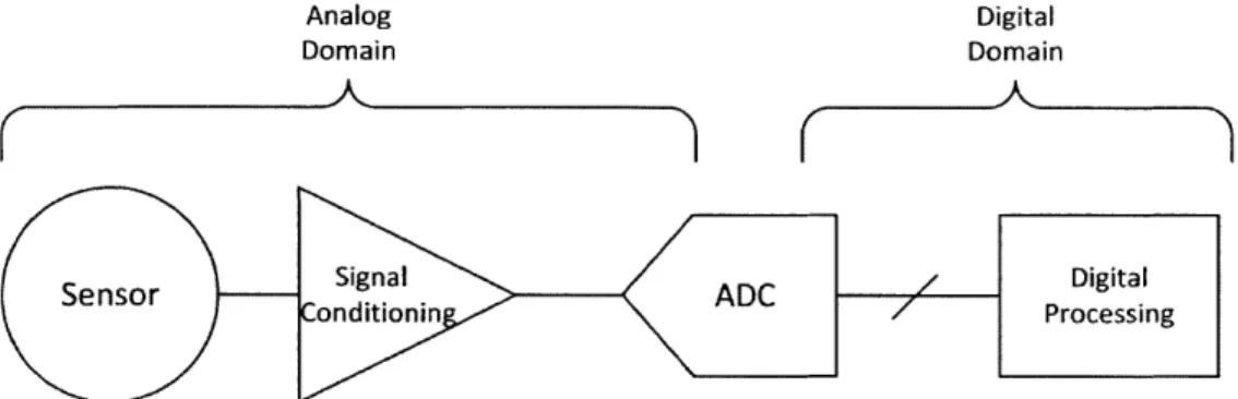
The signal chain of a typical electronic system with a real-world, analog input signal is illustrated in Fig. 1-1. The analog signal is sensed and transduced into an
electrical signal by a sensor. Next, the analog, electrical signal is conditioned and
processed (amplified, filtered, etc.) in the analog domain before being sampled and converted into a stream of bits by an ADC. The stream of bits is then sent to a
digital back-end or a computer to undergo further signal processing. Over the past few decades, we have observed that the prevailing trend in the field is to minimize
the amount of processing that is done in the analog domain, and to move as much processing as possible to the digital domain. This shift is driven by two main forces, one due to technology scaling, and the other is the drive to manage complexity as
systems scale in size and scope. From the technological standpoint, device scaling has
benefited digital circuits tremendously. Scaling has increased the speed and power efficiency of digital circuits significantly. However, with scaling, the supply voltage
and intrinsic gain of transistors keep reducing from one process node to another, which affects the performance of the analog blocks adversely. Thus, the trend has
Analog Digital
Domain Domain
A A
Sensor n ADC Processing
Figure 1-1: Block diagram of a typical signal-chain for electronic systems.
been to minimize the signal conditioning and processing in the analog domain, and
to shift the bulk of signal processing tasks to the digital domain.
The second motivation for minimizing the amount of signal processing that is done in the analog domain is the necessity to manage design complexity and to increase
design reuse. As systems keep getting more and more complex, it is valuable to have access to raw data that can use the most up to date advancements in new
digital processing techniques or software updates. In many applications, such as
medical or communication systems, it may be difficult or cost prohibitive to physically
upgrade the analog hardware, but updating the digital processing algorithms (e.g. by updating an FPGA or microcontroller) is feasible. One example of such a system is the cochlear implant - the analog blocks in the cochlear implant are usually made to be simple as possible, and most of the processing is done in the digital blocks that are
easily re-programmable and that can updated as new speech processing techniques are invented. From a design re-use perspective, analog systems are highly application
specific and cannot be ported or scaled easily from one application to another. Thus, for every application, significant design time needs to be dedicated for the design of the analog processing blocks. Digital systems, on the other hand, due to the
advancements in hardware description languages (HDLs), have enabled increasing amounts of design reuse from one application to another.
Both these reasons outlined above keep moving the boundary between the digital and analog further into the analog domain (i.e. minimized the processing done in the
Power Single Channel ADC Time-Interleaved ADC N=4 N=3 N=2 N = I Bandwidth
Figure 1-2: Plot of power consumption vs. input signal Nyquist bandwidth. The
curved line shows the expected power growth if a single channel ADC is used to
achieve increasing bandwidths. The linear line shows the expected power consumption of an ideal time-interleaved ADC with increasing bandwidths (with power of overhead circuitry to implement time-interleaving excluded).
analog domain, and move as much processing as is feasible into the digital domain).
This places an increased burden on the ADC. ADCs need to be faster (i.e. convert more samples per second) in order to be able to digitize signals at higher
frequen-cies, be very energy efficient, and operate at higher resolutions (i.e. encode more
information per sample).
1.1
Time-Interleaved ADCs
As more and more signal processing is moved to the digital domain, the need for
high-accuracy, and high-speed ADCs that operate in an energy efficient manner
be-comes increasingly important. One metric to compare the performance of different
ADCs is to use the energy-per-conversion-step figure-of-merit (FoM) [1]. Typically, as the number of conversions per second or the resolution of the ADC (i.e. the
num-ber of distinct digital levels) increases, so does the energy consumed per conversion.
However, the increase in the power consumption of an ADC is usually super-linear
in Fig. 1-2. As the bandwidth of the input signal is increased, the corresponding
power consumption of the converter increases much more quickly [2,3]. For example, consider a SAR ADC, where the total conversion time per sample is given by,
tclk - tsamp + N (tsettie + tComparator + tiogic), (1.1) where N is the number of bits of the converter. In order to increase the speed of the
ADC, a few or all of the variables in Eq. 1.1 above need to be reduced. In order to
reduce the DAC settling time, faster references are needed that consume significantly more power. Low power, static-current free latch based comparators may need to
be replaced by power hungry, current-mode comparators. Devices within the logic circuits will need to be upsized in order to reduce logic delays. Fundamentally, as
the various components in an ADC approaches the limits of a particular technology, demanding an increase in operation speed comes at a disproportionately greater
in-crease in power consumption. As such, it is becoming more energetically impractical
to build ADCs with increasing input signal bandwidths and with higher resolutions.
One effective method to increase the sampling speed of an ADC without
incur-ring a large energy penalty is to use more than one ADC in parallel. In Fig. 1-2, if 2 converters were used instead of 1, the increase in power consumption (denoted by the
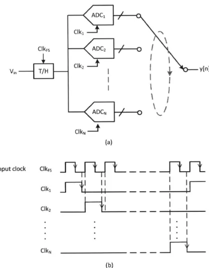
horizontal dotted lines), can be linear, if the extra power overhead to implement time-interleaving is excluded. This architecture is commonly known as time-time-interleaving and was first presented in [4]. A block diagram on a time-interleaved ADC is
illus-trated in Fig. 1-3. In a time-interleaved ADC, N ADC channels, each operating at a sampling frequency
f,
are used to achieve an effective conversion speed of N -f,
as illustrated in below. Therefore, in a time-interleaved ADC, each channel may operate at a slower, but more energy efficient conversion rate, but together achieve a highereffective conversion rate.
The importance of time-interleaving in achieving state-of-the-art performance can
be seen by observing the ADC papers presented at the International Solid State
ADC, Clk,
ADC20
100101001
Analog Input
4,
2 Digital OutputCIkN
Figure 1-3: Block diagram of a time-interleaved ADC.
(VLSI) over the years. Fig. 1-4 shows a graph with the Schreier FoM vs Nyquist
sampling frequency for all ADCs presented at ISSCC and VLSI from 1997-2014 [5].
The Schreier FoM is defined as,
FOMSchreier = SNDRdB + 10-
log
1 0(
7 ,(1.2)
(Pwhere BW is the maximum input signal bandwidth and P is the power consumption of the converter. The filled markers indicate the ADCs that utilize time-interleaving in their design. It is clear from this graph that in order to achieve very high sampling
speeds in an energy efficient manner, time-interleaving is an increasingly important
design paradigm.
While time-interleaving enables higher conversion rates in a given technology, it
is not without challenges. First, there is an area and energy overhead that comes
with utilizing a time-interleaved architecture. Having more channels requires more
die area. Having more channels also requires some auxiliary circuitry such as a
multi-phase sampling clock generation circuits, which adds an energy overhead.
chan-*ISSCC TI MVLSI TI Msscc
0
0 0 0 01 0 8 0 180 170 160 150 -140 -130 - 0 0 0 0 110 1 1.E+04 1.E+05 0 - 0 , - __ _ .. E %\\. 00 0 , o 0 QEE m %%%00 @00 0 C~:Q'~ 0 040 %%~ 0 0 0~0
9 @% 0 0 90 0 0 13 0oc 0 0 0 0 000
0
Figure 1-4: Plot of Schreier FOM vs Nyquist sampling frequencies for all ADC papers
presented at ISSCC and VLSI from 1997-2014.
nels further complicate the implementation of time-interleaved ADCs. Mismatch
between channels, such as gain mismatch, offset mismatch, and sampling clock skew
between channels can degrade the overall ADC performance [6]. Of these issues,
sam-pling clock skew between channels is the most challenging problem in time-interleaved
ADCs with high resolution and high sampling rates. There are a few sources of
sam-pling clock skew between channels. Mismatches in the samsam-pling clock paths and
logic delays are the most obvious. Input signal routing mismatch and resistive and
capacitive (RC) mismatches of the input sampling circuits also cause sampling clock
skew.
The sampling clock skew can be mitigated by various calibration techniques.
Pre-vious calibration techniques employ either sampling clock delay adjustment
tech-niques [7] or by digital correction of output data [8,9]. The timing adjustment requires
adjustable delays that can result in increased sampling jitter [7]. The increased jitter
degrades the SNDR at high input frequencies and cannot be compensated by
cali-bration. On the other hand, the digital calibration of output data requires complex
0
HDJ
0
U-120
1.E+06 1.E+07 1.E+08 1.E+09 1.E+10 1.E+11
fsnyq [Hz]
L. . .a --- ---
---interpolation. It is useful to note that many of the sampling clock skew calibration
techniques have been published in recent years, indicating that sampling clock skew calibration is an important current research area in ADC design.
In this thesis, we have developed a much simpler calibration circuitry and
al-gorithms for sampling time skew compared to previous techniques that have been published in the literature. We explore two proposed techniques to mitigate
sam-pling clock skew: i) a rapid consecutive samsam-pling technique whereby two samples of the input are acquired with a short delay between them for each channel in at
time-interleaved ADC, and ii) and input signal programmable delay technique whereby the delay of the input signal is controlled such that it is realigned with the sampling edge of the sampling clock with time-skew. We explore both techniques using behavioral
simulations. In both methods, the main goals are to avoid the increase in jitter and to minimize the complexity of the calibration method such that the impact on the
total noise and power consumption in the analog circuits can be made negligible.
1.2
Thesis Organization
This thesis is organized as follows. In Chapter 2 we theoretically analyze the various
errors that are present in time-interleaved ADC systems. In Chapter 3 we discuss the major sources of sampling clock skew in time-interleaved ADCs. In this chapter we
also explore previous work in the literature that propose methods for the detection
and mitigation of sampling clock skew in time-interleaved ADCs. Chapter 4 describes the calibration methods proposed in this research. Chapter 5 describes the circuit
design of a prototype ADC with our proposed sampling clock skew calibration scheme. Chapter 6 summarizes the results from the prototype ADC. Future research directions
Chapter 2
Operation of Time-Interleaved
ADCs
In Chapter 1, we described the importance of time-interleaving architectures in order
to build ADCs with higher resolutions and that operate at continually increasing speeds. In this chapter, we explore the operation of time-interleaved ADCs in more
detail. Specifically, we begin by analyzing the operation of a Nyquist sampling rate
converter in the time and frequency domains. This analysis will set the stage for the theoretical analysis of a time-interleaved system in which each channel is sampling
at below the Nyquist sampling frequency of the combined time-interleaved system.
More importantly, the analysis presented in this chapter will allow us to understand the effects of mismatches between channels on the operation of the time-interleaved
system. We conclude this chapter by exploring the various errors that plague
time-interleaved systems and their respective effects on the overall performance of the ADC system.
All Nyquist-rate ADCs can be reduced to a model with three main blocks: an
anti-aliasing filter block, followed by a sampling block and a quantizer block, as
illustrated in Fig. 2-1. The anti-aliasing filter block ensures that the input signal is
band-limited to below the Nyquist frequency, which is half of the sampling frequency of the ADC, in order to prevent aliasing that can degrade the performance of the
10101110
Analog Input
Digital Output
Anti-aliasing
Sampler
Quantizer
Filter
Figure 2-1: Block diagram of a typical Nyquist-rate ADC.
output of the sampling block is then input into the quantizer that quantizes the sampled continuous time signal in order to generate a digital output corresponding to the sampled continuous time level.
2.1
Single Channel Sampling
Before analyzing the operation of a time-interleaved ADC, we begin by analyzing an single channel ADC. In a single channel architecture, the continuous time input signal is sampled uniformly in time. A simplified version of the sampling process is illustrated in Fig. 2-2, where x(t) is the continuous time input signal, d(t) denotes the continuous time delta train, x (t) is the sampled continuous time signal, and x [n] is the discrete-time sampled signal. For the rest of the analysis in this section, we make two simplifications:
1. The sampling operation is performed using a delta train.
In real implementations, the input signal sampling is carried out by a track-and-hold circuit block that is more accurately modeled using a square wave or a periodic rectangular pulse signal. The analysis of such a sampling block, modeled using a zero-order-hold (ZOH) filter is described in [10] but is omitted in the analysis in this chapter for algebraic simplicity. It is important to note that this simplification does not affect the analysis or insights obtained in any substantial way.
x(t))
C/D
-+xs[n]
Figure 2-2: Block diagram of a sampling system.
2. The sampling operation is modeled as a continuous time block.
In reality, the output of the sampling block is a discrete time signal. This is illustrated in Fig. 2-2 where the continuous-to-discrete time block converts the
continuous time signal to a discrete time signal. In the following analysis, we
analyze the system only in continuous time, i.e. at the output of the multiplier. Mathematically converting a continuous time sample to a discrete time sample,
x,[n], is easily done via a substitution given by,
x,[n] = x,(nT), (2.1)
where n is an integer. However, in order to not be weighed down by notation, we will perform all the analysis in the following section in continuous time and
take the output of the sampler to be x,(t).
2.1.1
Single Channel Sampling in Time-Domain
The continuous time signal x(t) is sampled uniformly in time with a sampling period
of T using the delta train, d(t) which is given by:
00
d(t) = 6(t - kT). (2.2)
x(t)
0
I -2T -T
d(t)
0 T 2T 3T t
Figure 2-3: Time-domain representation of a continuous a delta train function, d(t).
- I - I
'I-x~(t)
I- ~4
I I I I I I I I -2T -T 0 T 2T 3T tsignal, x(t), sampled using
written as,
xS(t) = x(t) -d(t)
(2.3)
- E x(kT)6(t - kT), k=-oo
which is the delta train weighted by the samples of x(kT). The sampling process in time-domain is illustrated in Fig. 2-3.
2.1.2
Single Channel Sampling in Frequency-Domain
The sampling operation described in the time-domain above can also be analyzed in the frequency domain (and is often quite instructive). From the multiplication
property of Fourier transforms, the multiplication of x(t) and d(t) in the time-domain results in the convolution of X(jw) and D(jw) in the frequency domain, whereby
X(jw) and D(jw) are the Fourier transforms of x(t) and d(t) respectively. Hence, X,(jw) can be expressed as,
X,(jw)
=X(jw) * D(jw)
(2.4)Furthermore, we know that the delta train in the frequency domain is just a scaled
Xcjw)
Dow)
Xs/co)
-x
0
_ -27 0 27 -21 0 2rY T T T T T
Figure 2-4: Frequency-domain representation of a continuous signal, X(jW), sampled using a delta train function, D(jw).
be written as,
D(j) =- 6
W -
(2.5)T T
Since the convolution of a signal with an impulse train results in a shifted and summed version of the signal, the frequency response of the sampled signal, X,(jw), is given by,
1 X( 2i7rk 2(W (2.6)
X3(jW) = X
E
~
T),(2)k=-oo
The spectrum of the sampled signal is illustrated in Fig. 2-4. As long as the
input signal is band-limited to the Nyquist frequency, there will not be aliasing in the frequency response of the sampled output.
2.2
Time Interleaved Sampling
As described in Chapter 1, a time-interleaved ADC is made up of a number of N
channels or sub-ADCs. Each of the channels is used to sample the input signal in sequential manner such that the effective sampling rate of the system is N times
greater than the sampling rate of each individual channel. In this section, we look
at the sampling operation of a time-interleaved ADC and describe how by summing the sampled outputs of each of the channels, we can indeed achieve a higher effective
62(t)
x(t) +
y(t)
Figure 2-5: Block diagram of a N-way time-interleaved sampler. The delta trains, di(t), are used to sample the i-th channel and are delayed by T/N from each other.
2.2.1
Multi-Channel, Time-Interleaved Sampling in Time
Do-main
A higher effective sampling rate can be achieved by ensuring that the sampling
in-stance of each channel is distributed equally in time. As in the previous section, assuming that sampling of the input signal is performed using delta trains, the block
diagram of an N-channel, time-interleaved sampler is illustrated in Fig. 2-5. In this block diagram, each channel is sampled with a shifted delta train, di(t). The sampled
signals are then summed to produce the output, y(t). The delta train associated with the i-th channel in an N-way time-interleaved ADC can be expressed as,
di(t) n6 t - kT - i , (2.7)
k=-oo
The sampled signals x,,i(t) for each channel is then given by,
x,,i(t) =x(t) - di(t)
= : x kT + Ti) - t - kT -- i .28
k=-oo
The output of the time-interleaved sampling system is y(t), and can be expressed
as, N y(t) = ( x,,(t) (2.9)
E
x (kT + i )6 t-kT- i). i=1 k=-ooBy changing the variables of the summation and some algebraic manipulation, the
equation above can be rewritten as,
y(t)= X (m - (t - m ). (2.10)
By comparing Eq. (2.10) above to that of Eq. (2.3), we can see that the input signal
is sampled with a sampling period of -, which implies that the effective sampling
rate of the time-interleaved system is N times higher than that of the individual channel. The increased effective sampling rate of the time-interleaved system is more
easily observed visually in Fig. 2-6. In this illustration, a 4-way time-interleaved system is shown. The delta train dt,i(t) is the sum of the delta trains for each of
the channels. The delta train of each of the channels is separated by a delay of T/4
from each other, where T is the sampling period of each channel. The time domain
output, x,(t) shows the summed output of the time-interleaved sampler, in which the input signal appears to be sampled with a sampling period of T/4 rather than
T, showing that time-interleaving can effectively increase the sampling rate by the
dti(t)
4LX
-2T -1 0 T 2T 3 t -2T -4w 4 : 4 -4 4 'II 'II 'II 0 1 a a 4 4 4o
Channel 1 A Channel 3 O Channel 2 X Channel 4Figure 2-6: Time-domain representation of a 4-way time-interleaved system. The sampling period of each delta train is T, but the delta train for each channel is shifted by T/N from each other. The sampled output, x,(t) appears to be sampled with a sampling period of T/4.
2.2.2
Multi-Channel, Time-Interleaved Sampling in
Frequency-Domain
While the time-domain analysis presented above is useful in illustrating the operation of an ideal time-interleaved ADC, understanding the issues in real time-interleaved ADCs is more readily achievable by analyzing the operation of the time-interleaved
ADC system in the frequency domain.
As expressed in Eq. 2.4, the Fourier transform of x8,(t), which is the sampled output of each channel, can be expressed as,
Xs,i(jw)
=X(jw)
*
Di(jo),
(2.11)where Di(jw) is the time-shifted delta train signal. Using the time-shifting property
of Fourier transforms, Di(jw) is given by,
Di(jw) = D(jw) - e-'i (2.12)
x(t)
0
4 ) It
Given the above result, the Fourier transform of the sampled signal for each
chan-nel, x,,, is given by,
X,i(jw)
=X(jw) * D(jw) - e-j.
Tk=-oo
(2.13)
-ew-
ik The Fourier transform of the multiplexed output of the time-interleaved system,
Y(jw) is then given by, N Y(jw) = XS'i(jw) N 1o
TE
:
LX
(w
i=1 k=-oo (2.14)Eq. 2.14 can be recast as,
1
Y(j) =
27rk \E(jw)T) -Ej), (2.15)
X
(j(
w where E(jw) is defined as,N
E(jw)
=e
N i1 N - e-Z2 k i i=1 (2.16){
N,when k/N is an integer
0, elseFrom Eq. (2.16), we can observe that for integer values k/N, E(jW) evaluates to N, and for non-integer values of k/N, E(jw) evaluates to zero. Given the result above, we can rewrite Y(jw) as follows,
N
0Q/w
Y(jW) = T
X j(
- 27rm N\ ) , where m= k (2.17)27rk
T
By comparing Eq. (2.17) to Eq. (2.6) above, we can see that time-interleaved
sampling produces the same output as a single-channel system with a sampling period
of T/N instead of T. Thus the time-interleaved system has an effective sampling
period of T/N rather than T, which corresponds to an increase in the sampling frequency by a factor of N, the number of channels in the time-interleaved system.
The way in which time-interleaving results in an effectively higher-sampling system
is more intuitively explained using diagrams. In Fig. 2-7, the frequency representation of a two-way time-interleaved systems is shown. In a two-way time interleaved system, the output of each channel is,
= 0 (W - 27rk . Xfoj ) k=-coa s (e T X,, of m)
= E
X j(W
-
e-AD
(2.18)
k=-oo TE X (j(W - T - e-s k=-ooIn the equation for X,,e((), for all odd values of k, the exponential e - evaluates to -1, while for all other values of k, the exponential e- I evaluates to 1. From Fig.
2-7, we can clearly observe, when the output of both channels are summed, in an ideal
situation, the odd images of the spectrum of X(jo)
cancel
each other and we are only left with the spectrum of X(jw) spaced by T/2. As a result, Y(jw), which is the sumof X,,,O(jw)
+
X,(),results in a spectrum with no aliasing.2.3
The Effect of Channel Errors on the
Perfor-mance of Time-Interleaved ADC Systems
In the previous section we described how a time-interleaved system can be used to achieve a higher sampling speed for the entire system. In other words, we saw how N
channels each sampling at
f,
can be used to mimic a single channel running at N-f. This increase in performance is achieved by employing parallelism and requires the___________________________ I
-27c
T0
27E
TXsouwco)
-67E
-47E T T--27E T 02 T0
-6a
-41
T
T
W
AYUfw)
-47E
-2at
T T
0
2
47
.61E
T T T I4a
6a
T TFigure 2-7: Frequency-domain representation of a 2-way time-interleaved system. While the spectrum of each of the channels show aliasing in the frequency spectrum, the summed output does not suffer from aliasing. The images centered at tir, 37r,
...
from the odd and even channels (denoted using a shaded image) cancel each other out, leaving the resulting spectrum free of aliasing artifacts./V
use of four separate ADCs. In real implementations, there will always be systematic errors between the channels. As a result, in real time-interleaved systems, errors such
as offset mismatch, gain mismatch, and sampling clock skew between ADC channels will result in the performance degradation of the overall time-interleaved system. In
this section, we look at the effect of ADC channel errors on the overall time-interleaved
ADC performance.
2.3.1
Offset Mismatch Between Channels
The effect of offset mismatch between channels in a time-interleaved ADC can be modeled as an additive voltage source, V,j. A block diagram that includes offset
mismatch between channels is illustrated in Fig. 2-8. The presence of offset in itself
does not pose a major problem for the ADC. If the offset for all channels are the same and input signal independent, the offset error can be easily corrected in the
digital domain or even ignored. However, when the offsets between channels are mismatched, it causes a time-varying error in the time-interleaved system, which
leads to the presence of spurious tones in the frequency spectrum of the output of the
time-interleaved system.
The block diagram in Fig. 2-8 is used to model the output of each channel. By assuming a different offset voltage, V,, of up to 10 LSB for each 12-bit resolution
channel, the time domain error resulting from offset mismatches is shown in Fig. 2-9.
If we further assume that the variation in the offset of each ADC is independent of
the input signal characteristics, the errors introduced by offset mismatch between
channels is constant over the signal period, i.e. the offset mismatch produces fixed
amplitude and frequency noise that is independent of the sampling frequency or the input amplitude of the time-interleaved ADC.
We can evaluate the effect of offset mismatches in the frequency domain by eval-uating the Fourier transform of x,,i(t). With offset error, x.,i(t) now becomes,
V0,1
-}- ADC,
VO,2 Clk,
ADC2 --
-1L,
100101001Analog Input C4r2 Digital Output
VO,N
CIkN
Figure 2-8: Block diagram of a time-interleaved ADC with offset mismatch between channels modeled as an additive voltage source, V,,, at the input of the i-th channel.
2000
1000-o
-1000 -2000 0 C/) (b) -2 W 2U 10--10 0.1 0.2 0.3 0.4 0.5 0 0.1 0.2 0.3 0.4 0.5 Time (ps)Figure 2-9: Behavioral simulation results of the time domain error due to offset mismatches between channels. The plot in panel (a) shows a 12-bit output of a 4-way time-interleaved ADC with offset mismatch between channels. The graph in panel
(b) shows the error in LSBs of the time-interleaved system with offset mismatch from
the ideal, expected output code when no offset mismatch between channels is present.
j,-The Fourier transform of x,,i with offset is then given by,
Xs,i(jw) = (X(jw) + Vo,j) * Di(jw)
1
(w
2k)) .wlik V D(2.20)= T E X (j(W T ) - N + Vo,j - Di(jw). k=-oo
Using Eq. 2.17, the sum of the output of all the channels can then be expressed
as,
N * / N N
Y(j)27rm + JW) (2.21)Voj - D+(
From equation 2.21, we can expect that the offset error shows up as tones in the frequency domain at intervals of 1/T (since Di is periodic in 1/T), where T is the
sampling rate of each channel. The location of these spurs in the frequency domain are at,
f
7,O =i .
f
8 where i = 1, 2,3, ... (2.22)where
f,
is the sampling frequency of each interleaved channel.An example of the effect of offset mismatch on the time-interleaved system us-ing behavioral simulations is shown in Fig. 2-10. Here, a frequency spectrum of a
simulated 4-way time-interleaved ADC is shown with each channel having a different offset. The spurious tones appear at multiples of the channel sampling frequency as expected from the theory.
Again, it is important to note that the tones caused by the offset mismatch be-tween channels is independent of the input signal and only dependent on the channel
sampling period and the offset mismatch between channels.
2.3.2
Gain Mismatch Between Channels
The effect of gain mismatch between channels in a time-interleaved system can be modeled by using a gain element with gain values, Gi, for each channel. A block
0 CL -25--50 -75--100 -125
Spurs due to offset mismatch
2f, 0
Frequency
Figure 2-10: A frequency spectrum of the output of a behavioral simulation of a 4-way time-interleaved ADC with offset mismatches between channels. The spurs at f,/2 and
f,/4
are due to the offset mismatches between channels in the time interleaved ADC.-G, ADC,
Clk,
ADC2
100101001
Analog Input 2 Digital Output
0__ GN ADCN
CIkN -
-Figure 2-11: Block diagram of a time-interleaved ADC with gain mismatch between channels modeled as an gain block with gains, G,j before the input of the i-th channel.
is illustrated in Fig. 2-11.
The block diagram in Fig. 2-11 is used to model the output of each channel. To simulate the effects of gain mismatches between channels in a time-interleaved ADC, behavioral simulations are run for a 4-way time-interleaved ADC with different gains,
Gi, of up to t5% for each channel. The time domain error resulting in the gain
mismatches between channels is shown in Fig. 2-12. The time-domain error plot shows that the error is greatest at the peaks an troughs of the output signal. This makes intuitive sense as the error between a channel with a non-unity gain and an
ideal channel with unity gain is greater as the input signal amplitude increases.
As in the case with offset mismatches between channels, it is instructive to analyze
the effect of gain mismatches between channels in the frequency domain. This can be done by writing the Fourier transform of x,,i with the gain elements included.