HAL Id: lirmm-03168361
https://hal-lirmm.ccsd.cnrs.fr/lirmm-03168361
Submitted on 12 Mar 2021HAL is a multi-disciplinary open access archive for the deposit and dissemination of sci-entific research documents, whether they are pub-lished or not. The documents may come from teaching and research institutions in France or abroad, or from public or private research centers.
L’archive ouverte pluridisciplinaire HAL, est destinée au dépôt et à la diffusion de documents scientifiques de niveau recherche, publiés ou non, émanant des établissements d’enseignement et de recherche français ou étrangers, des laboratoires publics ou privés.
the adaptive compute node
Stefano Bernabovi, Michael Chapman, Philippe Naudin, Guillaume Devic,
Abdoulaye Gamatié, Gilles Sassatelli
To cite this version:
Stefano Bernabovi, Michael Chapman, Philippe Naudin, Guillaume Devic, Abdoulaye Gamatié, et al.. Deliverable D4.2 – Preliminary design specifications of the adaptive compute node. [Research Report] Cortus S.A.S; LIRMM (UM, CNRS). 2019. �lirmm-03168361�
D4.2 – Preliminary design specifications of the adaptive
compute node
Version 2.0 (2019) Final Public Distribution Main contributors:S. Bernabovi, M. Chapman, P. Naudin (Cortus); G. Devic, A. Gamatié and G. Sassatelli (LIRMM)
Project Partner Contact Information
Cortus S.A.S Inria
Michael Chapman Erven Rohou
97 Rue de Freyr Inria Rennes - Bretagne Atlantique
Le Génésis Campus de Beaulieu
34000 Montpellier 35042 Rennes Cedex
France France
Tel: +33 430 967 000 Tel: +33 299 847 493
E-mail: [email protected] E-mail: [email protected] LIRMM Abdoulaye Gamatié Rue Ada 161 34392 Montpellier France Tel: +33 4 674 19828 E-mail: [email protected]
Table of Contents
1 Introduction 2
2 Related Work 4
3 Asymmetric Architecture Prototype Design 5 3.1 Design Templates . . . 5 3.2 Implementation and Synthesis on FPGA . . . 8
4 Tailored Multithread Management 11
4.1 Memory Organization . . . 11 4.2 Thread Scheduling . . . 12 4.3 Implementation Methodologies . . . 13
5 Evaluation of the asymmetric architecture 14 5.1 Configuration Evaluation with ImgBW . . . 15 5.2 Configuration Evaluation with ImgBright . . . 15
6 Further considerations: non-volatile memory technologies 17
7 Conclusion and perspectives 19
Executive Summary
The goal of the CONTINUUM project is to define a new energy-efficient compute node model, which will benefit from a suitable combination of efficient compilation techniques, emerging memory, and communication technologies together with heterogeneous cores. Heterogeneous computing is a very promising solution to address the increasing energy-efficiency demand in modern multicore systems, by combining processors according to power consumption and performance trade-off. Compared to the technology review conducted in Deliverable 4.1 [49], the originality of the solution promoted here relies on the core technology of the Cortus partner.
The current deliverable presents a novel asymmetric multicore architecture based on very low power cores. A high-performance core is dedicated for sequential execution and multiple lightweight cores are devoted to parallel execution. In addition, a trade-off in terms of floating-point support in cores is considered for design cost reduction. A tailored flexible multi-thread execution model is defined for this architecture. A FPGA prototype is designed for the preliminary evaluation of the proposal. Even though this prototype does not integrate any non-volatile memory technology, this is highly advocated for the compute node design expected from the CONTINUUM project. The evaluation results already reported in Deliverable 3.2 [50] show the relevance of this choice.
Please note that the present deliverable is an updated version of Deliverable 4.2, based on the early lessons learned from Deliverable 4.3 (Implementation of the whole compute node model). The contents of the deliverable is mainly based on the results published in conferences or journals by the consortium members of the CONTINUUM project. More technical details could be found in the corresponding references.
1
Introduction
Heterogeneous computing usually refers to systems including various processing elements so as to meet both performance and power-efficiency requirements [27, 38, 43]. Typical heterogeneous architectures combine CPUs and compute accelerators such as Graphical Processing Units (GPUs). While the former is well-suited for executing sequential workloads and the operating system, the latter is rather devoted to massively regular parallel workloads, e.g., data-parallel algorithms.
Further examples are the Cell multiprocessor [24] developed by Sony, Toshiba and IBM, and the Llano processor [10] proposed by AMD. Cell combines a general-purpose core with streamlined co-processing elements that accelerate multimedia and vector co-processing applications, whereas Llano combines a quad-core CPU with a GPU.
The more recent ARM big.LITTLE technology [5] considers two different clusters: a big cluster composed of high-performance application processors used to execute heavy workloads; and a LITTLE cluster composed of low power application processors that are used for lightweight workload to save energy. By exploiting this feature, a suitable runtime can provide workloads with required performance while reducing the power consumption whenever possible.
The aforementioned architectures also referred to as asymmetric multicore architectures due to their core heterogeneity in terms of performance and power consumption [27] [32]. Despite their very attractive features for providing energy-efficiency, asymmetric multicore chips are still not mature and robust real-world commercial solutions [32].
In the current work, we devise a novel asymmetric multicore architecture comprising two execution islands: parallel and sequential. While the former is devoted to highly parallelizable workloads for high throughput, the latter addresses weakly parallelizable workloads. Accordingly, the parallel island is composed of many low power cores and the sequential island is composed of a small number of high-performance cores.
An original feature of our proposal is the usage of the cost-effective and inherently low power core technology provided by Cortus [2], one of the world-leading semiconductor IP companies in embedded domain. These cores are highly energy (MIPS/µW) and silicon efficient (MIPS/mm2)
compared to existing technologies. We believe the massive usage of such embedded cores deserves attention for achieving the energy-efficient architectures required for high-performance embedded computing. The architectural solution promoted here is similar to the CPU/GPU heterogeneous design paradigm. However, an important difference is that the parallel island, which plays the same role as the GPU, can suitably deal with both regular and irregular parallel workloads. In addition, both sequential and parallel islands support the same programming model, facilitating the job of programmers. GPUs require specific APIs such as OpenCL and CUDA, which are not necessarily supported by CPUs, requiring extensive software support. Compared to big.LITTLE technology that considers only application processors, here we combine application processors on the "big" side and micro-controllers on the "LITTLE" side. Such compact "LITTLE" cores (which are not intended to support a full OS) are key for aggressive energy optimization.
Another trade-off considered in our solution is the support of floating-point arithmetics, which benefits certain operations in embedded applications, e.g., matrix inversion required for Multiple Input / Multiple Output (MIMO), Fast Fourier Transforms (FFTs) which often suffer from scaling problems
in fixed point. As floating-point units can be expensive in terms of area and power in the considered very low power cores, it will be supported only by a subset of these cores.
A tailored lightweight and flexible multithread execution model is also defined in order to enable the management of programs executed on the proposed architecture, which is synthesized on FPGA. Given the helpful support of the Cortus Company regarding the design exploration task on synthesizable architecture descriptions, we decided to discard higher abstraction level approaches, e.g. cycle-approximate [6, 12, 34, 35], transactional level [44, 28, 29], analytical [16, 4, 3], and more generally model-driven engineering [18, 42, 17]. The very accurate assessments expected based on the target FPGA prototype will give us the opportunity to obtain more reliable insights.
Outline. The rest of this report is organized as follows: Section 2 discusses a few related work; then Section 3 describes the proposed multicore architecture and its implementation; Section 4 presents a preliminary proposal for multithread management on top of the architecture; Section 5 provides initial functional tests of the resulting FPGA prototype; Section 6 draws further design considerations, in particular about the integration of emerging non-volatile memory technologies; finally, Section 7 gives some concluding remarks.
2
Related Work
Several studies have been carried in academia on asymmetric architecture design. Hill et al. [22] applied Amdahl’s Law to explore different multicore chip architecture designs, namely symmetric, asymmetric and dynamic multicore (which enables multiple cores to work together for sequential execution). They combined an Amdahl’s software model with a simple hardware model based on fixed chip resources. They observed that asymmetric and dynamic multicore chips offer the highest speedups.
Morad et al. [33] evaluated asymmetric cluster chip multiprocessor for maximizing performance within a given power budget. Here, serial regions of multithreaded programs are executed on high performance cores while parallel regions are executed on both large and small cores. A theoretical analysis, validated by emulations, has been applied to make comparison with symmetric clusters. Authors observed that asymmetric design can provide a reduction of more than two-thirds in power for similar performance, while enabling more than 70% higher performance for the same power budget. Both [22] and [33] concluded their study by pointing out the fact that asymmetric architecture design exploration is deserving much attention for improved performance and power-efficiency in modern multicore systems. Reaching this goal obviously requires suitable program execution models capable of exploiting this asymmetric feature [27].
Kumar et al. [26] focused on the design of a processor in the context of single heterogeneous multicore architectures for performance and power trade-off. They showed that the most suitable heterogeneous chip multiprocessors comprise customized cores addressing different application characteristics. This interesting insight is relevant in our approach thanks to the high customizability of the adopted Cortus processors.
Suleman et al. [47] exploited compiler and OS support in asymmetric chip multiprocessor for accelerating the execution of critical sections (ensuring that only one thread is granted access to shared data at a time). Experiments showed that asymmetric design reduces the average execution time compared to area-equivalent symmetric design or asymmetric design without acceleration of critical section.
Ipek et al. [23] defined core fusion, which accommodates software diversity and incremental paral-lelization in reconfigurable chip multiprocessor architectures. Independent cores can be dynamically combined into a larger CPU (e.g., in order to accelerate serial code regions), or used as distinct pro-cessing elements (e.g., for executing parallel code regions). An interesting feature of core fusion is that no additional programming effort or specialized compiler support are required.
The present work shares similar motivations with above studies. Nevertheless, it relies on a novel prototype of asymmetric architecture built with cost-effective and very low power core technology. A special attention is given to the multithread workload management on such prototype so as to minimize the impact on energy-efficiency. We also show that the design trade-off about floating-point support plays an important role in performance improvement while benefiting of the inherent low power nature of cores. Unlike the big.LITTLE-like heterogeneous architecture considered in previous studies [5, 11, 13, 14, 39], we rather consider a heterogeneous design comprising more than 2 types of CPU cores. The benefit of such a design has been underlined in a few studies [31, 15, 37].
3
Asymmetric Architecture Prototype Design
3.1
Design Templates
The rationale for building the proposed asymmetric architecture follows the same principles as in previous works [22] and [33]. Given assumptions of Amdahl’s law, we consider that one powerful core is sufficient. Then, we combine it with several small cores. Fig. 1 shows three templates of candidate designs. The 4-core architecture depicted in Fig. 1(a) comprises one high-performance core, referred to as HP-Core; and three low power cores, i.e., micro-controllers, with various features: one with floating-point unit (LPF-Core) and two without (LP-Core). This provides an ISA diversity that meets the requirements of applications. Indeed, floating-point operations are not always present in embedded workloads. All four cores are connected to a shared memory via a hierarchy of crossbars as illustrated in Fig. 1(a). Table 3 gives the cost in area and power of these components.
(a) 4-core template (b) 7-core template (c) 10-core template
Figure 1: Various templates of proposed asymmetric architecture
Figs. 1(b) and 1(c) respectively describe two larger templates of our asymmetric architecture, com-posed of seven and ten cores. These templates result from a replication of the LP-Cluster comcom-posed by the three low power cores.
On-Chip Communication Strategies In a multiprocessor environment communication between the processors and peripheral resources quickly becomes a major design challenge.
There are three widely adopted strategies:
• Bus interconnect. In a simple bus architecture (see Fig. 2) there is a shared bus that is used by all masters to access all the slaves (the sharing is implemented with either tri-state buffers off-chip, or using wired-or techniques in an SoC). There is a simple contention control mechanism, preventing more than one master from using the bus at once. The bus mechanism can be reasonably sophisticated, offering a transactional model with the slaves providing a response at a different point in time from the request - avoiding blocking access to the bus for other masters while the response is being prepared. Very little additional hardware is required to attach to the bus and increasing the number of masters or slaves increases the hardware requirements linearly. The disadvantage of this architecture is that as the number of masters increases the throughput of the system drops dramatically.
Figure 2: Quadcore Cortus architecture with bus interconnect.
• Crossbar. In a Crossbar architecture (see Fig. 3) a multi-way multiplexer provides a path from each of the masters to each of the slaves. There is an arbitration mechanism preventing more than one master from accessing the same slave, however multiple simultaneous access are possible so long as they involve different masters and slaves. Increasing the number of masters or slaves increases the complexity, and size, of the Crossbar. The increase is exponential (O(n2))
[30] with increased masters and slaves. This architecture provides increased bandwidth and resource availability compared to the bus architecture, as unless there is contention for a slave there are no bandwidth constraints and the master can operate at the maximum rate supported by the slave and Crossbar infrastructure. More than 50% of the SoC area can be taken up with the Crossbar matrix in systems with many masters [51]. Another challenge with the on-chip design is timing closure. Complex Crossbar systems become unwieldy and there are long logic paths that mean it becomes increasingly difficult to reach the target operating frequency of the bus.
• Network-on-Chip (NoC). A NoC provides a shared path between network nodes (see Fig. 4). This can be a serial or parallel architecture. Each transaction is packetized and typically contains overhead such as source and destination addresses. The network interface may contain a FIFO allowing transactions to be stored, either until the network is ready to accept the packet or the node is ready to receive the transaction. This can increase the latency of transactions. In a highly congested network timing and real-time operation may become compromised, potentially leading to non-deterministic behaviour. There is a significant fixed overhead per node required to implement a network-on-chip (the Network Interface in the diagram), however this overhead scales linearly with increased nodes. This network interface can be of varying complexity according to the system design requirements, from simple hardware to insert a packet onto the network with the correct address headers to a complete store and forward system for a transactional network with a multiple depth FIFO to hold several messages in flight.
A Network-on-Chip solution isolates each node in its own timing bubble and the global timing constraints are specified and fully defined by the network design. However the nature of an NoC limits the bandwidth between systems, the resource must be shared - and divided equally
Figure 3: Quadcore Cortus architecture with crossbar interconnect.
- between all bus masters. This implies a reduced communication capacity between nodes compared to a Crossbar design.
Table 1: Summary of main characteristics of on-chip interconnects
Bus Crossbar NoC
Simplicity + + + + + +
Latency + + + + + +
Throughput + + + + + +
Throughput with increasing connections + + + + + +
Hardware overhead - - -
-Hardware overhead with increasing connections - - - -
-There is a trade-off between complexity (die area required, power consumption), transfer speed, latency and throughput are summarized in Table 1. Very simple systems can use a bus architecture, typically systems with one master (and perhaps a second master that takes control only occasionally) but as the complexity increases a Crossbar approach becomes attractive, allowing multiple masters to access multiple, shared, slaves. As the number of potential paths between each master and slave increases the complexity of the Crossbar infrastructure increases to a point that a large portion of the die is reserved for the Crossbar and timing closure becomes increasingly difficult. At this point an NoC approach becomes attractive, the cost (in terms of die area and power consumption) of the network attachment hardware and the increase in latency is comparatively less. Table 2 summarizes the above observations.
Table 2: Design choices according to communicating nodes
Bus Crossbar NoC single master node +
several master nodes +
many master nodes +
The point at which an NoC becomes necessary can be postponed by using a multi-level Crossbar system where the number of masters and slaves per Crossbar is reduced by using multiple levels of Crossbar. In the NoC the medium is shared between all nodes. In a Crossbar system there is a dedicated, switched, the path from each master to each slave. The key architectural difference between a Crossbar system and an NoC is the trade-off between space and time.
Our design templates illustrated in Fig. 1 adopt such a mechanism.
3.2
Implementation and Synthesis on FPGA
In order to implement a prototype of the proposed architecture design on FPGA, we consider a Genesys 2 board of Diligent [1]. It is an advanced development platform that relies on the powerful
Figure 5: Implemented asymmetric architecture
Kintex-7 FPGA of Xilinx (XC7K325T). This FPGA provides large capacity and performance. In addition, several useful built-in peripherals enable a wide range of additional applications.
Here, we implement an instance of the 4-core template (see Fig. 1(a)) so as to match the size constraints of Kintex-7 FPGA. Fig. 5 describes the corresponding synthesizable implementation. The generic HP-Core, LPF-Core and LP-Core cores are respectively implemented with the Cortus APSX2, FPS26 and APS25 cores. The APSX21is a new high-end multiple-issue, out-of-order CPU supporting floating-point computation. It was designed as an application processor with features such as precise exceptions, branch prediction and multiple threads of execution. Compared to other cores of Cortus, it provides a higher memory bandwidth due to wider memory buses. The FPS26 is an extensible 32-bit core featuring a single precision floating-point combined with excellent code density. As most Cortus cores, it relies on Harvard architecture with 2 × 4 GByte address space. It is suitable for creating complex embedded systems with caches, co-processors and multiple cores, e.g., in audio, vision, advanced control and communication applications. floating-point arithmetics benefits a number of algorithms in those domains. The APS25 core is similar to the FPS26, but has no floating-point unit. This reduces its complexity in terms of area and power, as a major part of embedded applications do not require floating-point calculations. There is a strict inclusion between the above Cortus cores in terms of instruction sets: APS25 is included in FPS26, itself included in ASPX2.
The remaining part of the system is composed of standard peripherals such as UART, counters, breakpoint handlers and interrupt controllers. A message box peripheral (referred to as MSGBOX in Fig. 5) is designed to enable communication between the different cores by means of specific interrupts.
The resulting architecture has been synthesized on the Genesys FPGA board [1] (see Fig. 6) for evaluation.
Figure 6: The Genesys FPGA board used for compute node prototype.
Table 3 provides an assessment of different design elements in terms of slice count for the Kintex-7 FPGA. Furthermore, gate count, area and power numbers resulting from a synthesis targeting an UMC 55nm ASIC technology. Here, HP-Core core is far more complex in area and power than LPF-Core and LP-Core due to its advanced features. On the other hand, the presence of floating-point support in LPF-Core makes this core twice costly than LP-Core. By taking into account the interconnect (used crossbars) and cores, we give an estimate for the three design templates (here, memory is not included in the estimation as it is assumed off-chip). An interesting observation is that the scalability of these templates does not dramatically degrade their cost in area and power, while performance improvement is expected thanks to more parallelism. This suggests that adding more cores for improved performance could improve the global energy-efficiency.
The implementation of the complete 4-core design shown in Fig. 5 occupies 71% of the total number of LookUp Tables (LUTs) on the FPGA. Preliminary evaluations showed that the instance of HP-Core used here is faster than LPF-HP-Core and LP-HP-Core in a range between 70% and 800% (according to floating-point calculations or not) at identical frequency.
Table 3: Design elements assessment
FPGA metrics ASIC metrics
Slices Gates Area (µm2) Power (mW)
HP-Core 122941 1471462 1341624 4 LPF-Core 7919 93083 134039 0.86 LP-Core 3981 47648 68613 0.42 Interconnect 7359 24736 119733 0,78 4-core 164653 1551905 4431142 6.48 7-core 196029 1762186 6092947 8.18 10-core 232573 1972467 7754751 9.88
4
Tailored Multithread Management
Having a suitable execution model is crucial for adequate exploitation of proposed asymmetric system design. First of all, we consider a multithread programming model, assuming programs written in C. A cooperative thread scheduling is adopted, i.e., a thread completes before switching to another thread on a given core (meaning no context switch). While this approach is less flexible for real-time workloads, it is simple and more effective for computation-intensive workloads. Multithread execution is eased here by giving threads a list of dependencies to be guaranteed by the scheduler. The scheduling is also dynamic, i.e., threads can be executed by any available core in any order when allowed. Thread declaration is static, thus fixed at compile time. A library of functions and data structures ready to use by the user is provided for thread scheduling.
In the next, the scheduler is executed on HP-Core, which plays the role of "master" core that assigns threads to "slave" cores (i.e., LPF-Core and LP-Cores) and itself.
4.1
Memory Organization
We separate program and data memories for each core. Two additional memory zones are reserved to shared memory and for the memory management unit (MMU) configuration. This makes it possible to compile the same program for different cores implementing different instruction sets. In Fig. 7(a), three different functions a(), b() and c() can be compiled differently, resulting in different machine codes, sizes and memory placements, but unchanged functionality. If a specific code fragment has to be executed by a specific core, the cpu_id() run-time function is used to indicate this core. At the data level, each core has its own data, stack and heap. To share data, a shared memory section is available, including a shared heap. For dynamic memory allocation, the smalloc() and sfree()functions are available. A basic lock mechanism for exclusive access is implemented in those functions. The MMU configuration for all the cores is stored in a dedicated memory section.
(a) memory organization (b) thread creation (c) thread execution
Figure 7: Multithreaded management approach
Since direct memory mapping is used and is the same for every core, this allows for memory saving, hence reducing information replication.
In the shared data, three status vector are provided:
• cpu_ready[4] to indicate if a core is ready,
• cpu_valid[4] to indicate to a core if data is valid and execution can be started, • cpu_assigned_thread[4] to store the address of the thread to execute.
Furthermore, a cpu_lock variable is available to implement exclusive access to shared resources.
4.2
Thread Scheduling
Threads and functions are represented by data structures:
• cFunction makes the link between a function and its physical address in memory. This is very important to support different instruction sets.
• cThread contains the reference to the function with its parameters, the return value, depen-dencies, status, execution time and further information.
Two creation functions populate these structures and link them in lists:
• cFunctionCreate(): takes a function pointer and a string tag, and associates them in a linked-list working as a look-up table in the heap memory. Each core must perform this creation to have its LUT in its heap!
• cThreadCreate(): takes a function string tag, the parameters, return value and dependen-cies and put them in a linked list in the shared heap memory. Parameters and return values are always casted void*. This created information is available to every core in the shared heap.
In Fig. 7(b), cFunctionCreate takes the address of a function and links it with the string tag function_a(blue solid arrows). Then, cThreadCreate takes the string tag to create a thread in the shared memory (blue dashed arrow).
When the two steps of creation are performed, the "master" core can start thread scheduling, and finally all cores can start execution. For this purpose, two methods are provided:
• cSchedulerExecute(): launches one iteration of the scheduler, which checks whether: – there are threads available in the thread list;
– dependencies are fulfilled;
– a core is available (cpu_ready[i] == 1);
If all conditions are satisfied, then a thread is assigned to a core. Its address is copied in cpu_assigned_thread[i]where i is the identifier of the target core. The core is signaled via an interrupt or by setting cpu_valid[i] to 1. cSchedulerExecute returns the identifier of the thread to be executed.
• cThreadExecute(): executes a thread after retrieving the function to be executed from the function list. When it has finished, it notifies the "master" core.
In Fig. 7(c), cSchedulerExecutes (on HP-Core) assigns the thread to LP-Core: cpu_ready[3] goes 0, cpu_valid[3] is set to 1 while the thread address is stored in cpu_assigned_thread[3](red solid arrows). Then, cThreadExecute (on LP-Core) takes this address and the control of the thread. It uses the function string tag to retrieve the address of the function and executes it (red dashed arrows).
4.3
Implementation Methodologies
When describing the above scheduler, we mentioned a "polling" approach which uses cpu_valid[] for signaling and an "interrupt" approach which relies on interrupt routines. The polling ap-proach consists of looking continuously at a memory location waiting for some value (in this case, cpu_valid[i] == 1). During idle phase, "slave" cores do nothing and "master" core runs the scheduler. All cores can run a thread. A corresponding pseudo-code is as follows:
00 if (cpu_id() == 0) { 01 do { 02 remaining = cSchedulerExecute(); 03 if (cpu_valid[0]) cThreadExecute(); 04 } while (remaining != 0); 05 } else {
06 do {
07 if (cpu_valid[cpu_id()]) cThreadExecute(); 08 } while (1);
09 }
This approach is way more simple, but less effective. In fact, the "master" core assigns a thread to itself and re-runs the scheduler only once this thread is completed.
The interrupt approach consists in notifying the core whenever an interrupt signals the start of execution. An interrupt is also sent to signal the end of execution, launching the scheduler. The interrupt routines will then call the execution functions. A corresponding pseudo-code is as follows:
00 void interrupt_handler(IRQ_MSGBOX_0Mto1S) { 01 msgbox[1]->req[0] = 0; 02 cThreadExecute(); 03 } 04 void interrupt_handler(IRQ_MSGBOX_1Sto0M) { 05 msgbox[0]->req[1] = 0; 06 cSchedulerExecute(); 07 }
Here, the routines shown for HP-Core and LPF-Core, exist for all four cores. This approach is more difficult to handle, but it is easily understandable and, if nesting interrupt is enabled, it is more effective. In fact, the "master core" can interrupt its assigned thread execution to run the scheduler and assign a new thread to a free core as soon as possible.
5
Evaluation of the asymmetric architecture
We evaluate the performance of the proposed architecture by considering two simple image processing programs:
• ImgBW (converting color to grayscale): this program takes a color image as input, where each pixel is characterized by three components (R, G, B) corresponding to red, green and blue; then, maps the three components into a single grayscale value by computing the weighted sum of component values (i.e., luminosity method).
• ImBright (brightness conversion): this program transforms a colored input image by doubling the luminance.
The program ImgBW manipulates floating-point numbers while ImBright does not. For their multithreaded execution, each input image is divided into four equal sub-parts, each transformed by a separate thread, i.e., four threads are executed: T0, T1, T2 and T3. The following core assignment order is considered respectively for these threads when all cores available: LPF-Core, LP-Core, LP-Core, and HP-Core.
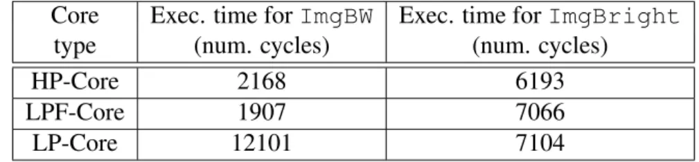
Table 4 reports the total execution time (i.e., program and scheduler) in terms of CPU cycles, for dif-ferent configurations (or scenarios) of the asymmetric multicore system for ImgBW and ImgBright. All the scenarios are run at the same frequency. The average time taken to execute a thread on each core is given in Table 5.
5.1
Configuration Evaluation with ImgBW
In Table 4, the best performance for ImgBW is provided when the four threads are executed only by the HP-Core and LPF-Core cores. This is explained by the fact that both cores integrate a floating-point unit. In addition, the HP-Core includes further features that makes it powerful (e.g., branch prediction and larger cache). The scenario considering only HP-Core is just below the previous one in terms of execution time. The reason lies in the fact here the execution of threads is serialized. It is interesting to observe that the configuration composed of all cores and the one composed of LPF-Core and LP-Cores lead to almost similar execution times. This shows the non negligible penalty due to LP-Core in presence of floating-point computation. Indeed, as reported in Table 5, the corresponding average thread execution time is higher. As a result, the worst scenario is the one composed of LP-Cores only (see Table 4).
Table 4: Configuration evaluation on programs
Configurations Exec. time for Exec. time for ImgBW(cycles) ImgBright(cycles) HP-Core & LPF-Core 8171 Not Considered
Only HP-Core 12536 9886
All cores 14861 16894
LPF-Core & two LP-Cores 14945 28455 Two LP-Cores 26309 Not Considered
On the other hand, we notice that the above results depend on the workload complexity assigned to each thread. For instance, let us crop bigger size of an input image, i.e., 3/4 of the image, and assign it to HP-Core and LPF-Core for execution. The remaining part is assigned to LP-Cores. We therefore obtain a reduction of 41% of the total execution time in comparison with the "All cores" configuration in Table 4.
Table 5: Average time per thread for each core type Core Exec. time for ImgBW Exec. time for ImgBright
type (num. cycles) (num. cycles)
HP-Core 2168 6193
LPF-Core 1907 7066
LP-Core 12101 7104
5.2
Configuration Evaluation with ImgBright
When considering ImgBright, a different behavior is obtained with LP-Cores in Table 4 as they can be fully leveraged for threads execution. For this non-floating-point program, since all cores can be used for maximum performance, we only compare the three most relevant configurations.
The average thread execution times for LPF-Core and LP-Core are closer in Table 5, while HP-Core is faster. Then, the shortest execution time is provided by the scenario including all four cores, i.e., higher parallelism level. Reducing the core count in other scenarios leads to longer execution times. In the above evaluations, we notice that the scenarios consisting of a single HP-Core only can lead to far better execution times as this high-performance core is supposed to run at a frequency twice faster than those of LPF-Cores and LP-Cores. The results reported above consider the same frequency for all configurations.
Beyond the above experiments, which targeted the preliminary system prototype, further evaluations have been carried out on an extended 7-core prototype [20]. They are presented in deliverable 5.2 of the CONTINUUM project.
6
Further considerations: non-volatile memory technologies
The previous architecture design could be extended for better energy-efficiency. In particular, the CONTINUUM project advocates the integration of non-volatile memory (NVM) technologies in the memory hierarchy [48, 39, 46]. As a matter of fact, NVMs are parts of the emerging technologies fore-seen for addressing the energy consumption issue in future technologies. A majority of current systems integrate volatile memories such as Static Random Access Memories (SRAM) and Dynamic Ran-dom Access Memories (DRAM). Unlike those memories, NVM favors a potential power consumption reduction by enabling a complete circuit power-down without losing data and logic states.
Table 6 summarizes the differences between candidate Magnetic Random Access Memory (MRAM) technologies [45], compared to the more standard SRAM technology. The Toggle MRAM technology is very mature but consumes more power than the other NVMs. Due to its voltage-controlled switching scheme, the Magnetoelectric Random Access Memory (MeRAM) requires a very low write current compared to the other technologies. The Spin Transfer Torque RAM (STT-RAM) and the Spin-Orbit Torque RAM (SOT-RAM) show almost the same overall performance and are very good candidates to be part of the cache memory hierarchy in Systems-on-Chip. The Thermal-Assisted Switching RAM (TAS-RAM) technology is the most reliable thanks to its magnetic tunnel junction structure, which allows excellent thermal stability, hence very good data retention.
Among the above NVM technologies, we consider the STT-RAM for integration in the cache memory hierarchy of the target design. We have been conducting a number of studies to evaluate the potential gain in energy consumption [50, 40, 7, 8, 9, 41], by using a analytical and cycle-accurate modeling as the corresponding memory devices are not yet mainstream on the market. The obtained results showed a promising improvement to the target system energy-efficiency. The gathered insights aim to be leveraged in the compute node design targeted by the CONTINUUM project. Finally, note that further opportunities on the exploration of NVM integration at the main memory level have been explored during the project [25, 21].
T echnology Cell size (F 2) Access time Write curr ent Endurance Maturity Adv antages / Drawbacks read/write SRAM 50–120 1–100 ns / 1–100 ns lo w 10 16 Commercialized (+) Maturity , access time (-) Current leakage T oggle 50 35 ns / 35 ns > 30 mA 10 15 Commercialized (+) Maturity (-) High po wer T AS < 50 30 ns / 30 ns A fe w mA 10 15 T est chip (+) Reliability (-) Access time STT < 50 2-20 ns / 2-20 ns 50 uA > 10 16 T est chip (+) Lo w po wer (-) Reliability MeRAM < 10 < 10 ns v ery lo w > 10 16 Prototype (+) Lo w po wer (-) Maturity SO T < 50 A fe w ns < 100 uA > 10 16 Prototype (+) Lo w po wer (-) Maturity T able 6: Magnetic memory technologies ver sus SRAM [45 ]
7
Conclusion and perspectives
In this deliverable, we presented a novel asymmetric multicore architecture based on cost-effective and very low power core technology targeting the embedded domain. This architecture combines a high-performance core suitable for sequential execution, and several lightweight low power cores devoted to parallel execution. A prototype of this architecture has been implemented on FPGA together with a tailored flexible multithread execution model. This is the first attempt to build an asymmetric multicore architecture based on the low power core technology of Cortus, which is one of the world-leading semiconductor IP providers for embedded domain. An energy measurement facility [39] has been adapted to the FPGA prototype.
A preliminary evaluation of our solution raises interesting insights regarding floating-point support in considered cores. The opportunity of customizing certain LP-Cores makes it possible to devise tradeoffs in terms of performance, area and energy efficiency. This type of customization is not limited to floating-point support and could very well be extended to other features such as cryptographic primitives or pattern-oriented computations, particularly useful for security or channel coding. Beyond the building blocks used in the implemented compute node prototype, the promoted design also features non-volatile memory technologies for an improved energy-efficiency. This is the aim of complementary studies carried out in the CONTINUUM project, based on a cycle-accurate system model in gem5 [7].
Future work includes a refinement of the proposed architecture with advanced workload management in order to leverage the features of the different cores for optimized performance. High-performance cores are known to be adequate for addressing compute-intensive workloads with predictable branching and high data-reuse. Low power cores are more memory-intensive workloads friendly. Exploiting such knowledge in core allocation to threads is a worth research direction. We already started to explore a candidate compiler-assisted approach for workload scheduling on such heterogeneous architectures [36]. Another worth-mentioning direction concerns the integration of machine learning techniques in the resource allocation decision process [19]. Finally, considering non-volatile memory in the main memory level is another opportunity to investigate.
References
[1] Genesys 2 Kintex-7 FPGA Development Board. https://www.xilinx.com/products/ boards-and-kits/1-cfdwjq.html, July 2017.
[2] Cortus SAS – Advanced Processing Solutions. http://www.cortus.com, July 2017.
[3] An, X., Boumedien, S., Gamatié, A., and Rutten, É. CLASSY: a clock analysis system for rapid prototyping of embedded applications on mpsocs. In Corporaal, H. and Stuijk, S., editors, Workshop on Software and Compilers for Embedded Systems, Map2MPSoC/SCOPES 2012, Sankt Goar, Germany, May 15-16, 2012, pages 3–12. ACM, 2012. doi: 10.1145/2236576.2236577. URL https://doi.org/10.1145/2236576.2236577.
[4] An, X., Gamatié, A., and Rutten, É. High-level design space exploration for adaptive applications on multiprocessor systems-on-chip. J. Syst. Archit., 61(3-4):172–184, 2015. doi: 10.1016/j. sysarc.2015.02.002. URL https://doi.org/10.1016/j.sysarc.2015.02.002.
[5] ARMbLtd. big.little technology: The future of mobile. 2013. URL https://www.arm. com/.
[6] Binkert, N., Beckmann, B., Black, G., Reinhardt, S. K., Saidi, A., Basu, A., Hestness, J., Hower, D. R., Krishna, T., Sardashti, S., Sen, R., Sewell, K., Shoaib, M., Vaish, N., Hill, M. D., and Wood, D. A. The gem5 simulator. SIGARCH Comput. Archit. News, 39(2):1–7, August 2011. ISSN 0163-5964. doi: 10.1145/2024716.2024718. URL https://doi.org/10.1145/ 2024716.2024718.
[7] Bouziane, R., Rohou, E., and Gamatié, A. How Could Compile-Time Program Analysis help Leveraging Emerging NVM Features? In EDiS: Embedded and Distributed Systems, pages 1–6, Oran, Algeria, December 2017. doi: 10.1109/EDIS.2017.8284031. URL https: //hal.inria.fr/hal-01655195.
[8] Bouziane, R., Rohou, E., and Gamatié, A. Compile-time silent-store elimination for energy efficiency: an analytic evaluation for non-volatile cache memory. In Chillet, D., editor, Pro-ceedings of the RAPIDO 2018 Workshop on Rapid Simulation and Performance Evaluation: Methods and Tools, Manchester, UK, January 22-24, 2018, pages 5:1–5:8. ACM, 2018. doi: 10.1145/3180665.3180666. URL https://doi.org/10.1145/3180665.3180666.
[9] Bouziane, R., Rohou, E., and Gamatié, A. Energy-efficient memory mappings based on partial WCET analysis and multi-retention time STT-RAM. In Ouhammou, Y., Ridouard, F., Grolleau, E., Jan, M., and Behnam, M., editors, Proceedings of the 26th International Conference on Real-Time Networks and Systems, RTNS 2018, Chasseneuil-du-Poitou, France, October 10-12, 2018, pages 148–158. ACM, 2018. doi: 10.1145/3273905.3273908. URL https://doi.org/10. 1145/3273905.3273908.
[10] Branover, A., Foley, D., and Steinman, M. Amd fusion apu: Llano. IEEE Micro, 32(2):28–37, March 2012. ISSN 0272-1732. doi: 10.1109/MM.2012.2.
[11] Butko, A., Gamatié, A., Sassatelli, G., Torres, L., and Robert, M. Design exploration for next generation high-performance manycore on-chip systems: Application to big.little architectures. In 2015 IEEE Computer Society Annual Symposium on VLSI, pages 551–556, 2015. doi: 10.1109/ISVLSI.2015.28.
[12] Butko, A., Garibotti, R., Ost, L., Lapotre, V., Gamatié, A., Sassatelli, G., and Adeniyi-Jones, C. A trace-driven approach for fast and accurate simulation of manycore architectures. In The 20th Asia and South Pacific Design Automation Conference, ASP-DAC 2015, Chiba, Japan, January 19-22, 2015, pages 707–712. IEEE, 2015. doi: 10.1109/ASPDAC.2015.7059093. URL https://doi.org/10.1109/ASPDAC.2015.7059093.
[13] Butko, A., Bessad, L., Novo, D., Bruguier, F., Gamatié, A., Sassatelli, G., Torres, L., and Robert, M. Position Paper: OpenMP scheduling on ARM big.LITTLE architecture. In MULTIPROG: Programmability and Architectures for Heterogeneous Multicores, Prague, Czech Republic, January 2016. URL https://hal-lirmm.ccsd.cnrs.fr/lirmm-01377630. [14] Butko, A., Bruguier, F., Gamatié, A., and Sassatelli, G. Efficient Programming for Multicore
Processor Heterogeneity: OpenMP versus OmpSs. In OpenSuCo, Frankfurt, Germany, June 2017. URL https://hal-lirmm.ccsd.cnrs.fr/lirmm-01723762. Held in conjunction with the 2017 ISC High Performance Computing Conference.
[15] Butko, A., Bruguier, F., Novo, D., Gamatié, A., and Sassatelli, G. Exploration of performance and energy trade-offs for heterogeneous multicore architectures. CoRR, abs/1902.02343, 2019. URL http://arxiv.org/abs/1902.02343.
[16] Caliri, G. V. Introduction to analytical modeling. In 26th International Computer Measurement Group Conference, December 10-15, 2000, Orlando, FL, USA, Proceedings, pages 31–36. Computer Measurement Group, 2000. URL http://www.cmg.org/?s2member_file_ download=/proceedings/2000/0004.pdf.
[17] Dekeyser, J.-L., Gamatié, A., Etien, A., Ben Atitallah, R., and Boulet, P. Using the UML Profile for MARTE to MPSoC Co-Design. In First International Conference on Embedded Systems & Critical Applications (ICESCA’08), Tunis, Tunisia, May 2008. URL https://hal.inria. fr/inria-00524363.
[18] Gamatié, A., Beux, S. L., Piel, É., Atitallah, R. B., Etien, A., Marquet, P., and Dekeyser, J. A model-driven design framework for massively parallel embedded systems. ACM Trans. Embed. Comput. Syst., 10(4):39:1–39:36, 2011. doi: 10.1145/2043662.2043663. URL https: //doi.org/10.1145/2043662.2043663.
[19] Gamatié, A., An, X., Zhang, Y., Kang, A., and Sassatelli, G. Empirical model-based perfor-mance prediction for application mapping on multicore architectures. J. Syst. Archit., 98:1–16, 2019. doi: 10.1016/j.sysarc.2019.06.001. URL https://doi.org/10.1016/j.sysarc. 2019.06.001.
[20] Gamatié, A., Devic, G., Sassatelli, G., Bernabovi, S., Naudin, P., and Chapman, M. Towards energy-efficient heterogeneous multicore architectures for edge computing. IEEE Access, 7:
49474–49491, 2019. doi: 10.1109/ACCESS.2019.2910932. URL https://doi.org/10. 1109/ACCESS.2019.2910932.
[21] Gamatié, A., Nocua, A., Weloli, J. W., Sassatelli, G., Torres, L., Novo, D., and Robert, M. Emerging NVM Technologies in Main Memory for Energy-Efficient HPC: an Empirical Study. working paper or preprint, May 2019. URL https://hal-lirmm.ccsd.cnrs.fr/ lirmm-02135043.
[22] Hill, M. D. and Marty, M. R. Amdahl’s law in the multicore era. Computer, 41(7):33–38, July 2008. ISSN 0018-9162. doi: 10.1109/MC.2008.209.
[23] Ipek, E., Kirman, M., Kirman, N., and Martinez, J. F. Core fusion: Accommodating software diversity in chip multiprocessors. In Proceedings of the 34th Annual International Symposium on Computer Architecture, ISCA ’07, pages 186–197, New York, NY, USA, 2007. ACM. ISBN 978-1-59593-706-3. doi: 10.1145/1250662.1250686.
[24] Kahle, J. A., Day, M. N., Hofstee, H. P., Johns, C. R., Maeurer, T. R., and Shippy, D. Introduction to the cell multiprocessor. IBM J. Res. Dev., 49(4/5):589–604, July 2005. ISSN 0018-8646. [25] Komalan, M., Rock, O. H., Hartmann, M., Sakhare, S., Tenllado, C., Gómez, J. I., Kar, G. S.,
Furnémont, A., Catthoor, F., Senni, S., Novo, D., Gamatié, A., and Torres, L. Main memory organization trade-offs with DRAM and STT-MRAM options based on gem5-nvmain simulation frameworks. In Madsen, J. and Coskun, A. K., editors, 2018 Design, Automation & Test in Europe Conference & Exhibition, DATE 2018, Dresden, Germany, March 19-23, 2018, pages 103–108. IEEE, 2018. doi: 10.23919/DATE.2018.8341987. URL https://doi.org/10.
23919/DATE.2018.8341987.
[26] Kumar, R., Tullsen, D. M., and Jouppi, N. P. Core architecture optimization for heteroge-neous chip multiprocessors. In 2006 International Conference on Parallel Architectures and Compilation Techniques (PACT), pages 23–32, 2006.
[27] Kumar, R., Tullsen, D. M., Jouppi, N. P., and Ranganathan, P. Heterogeneous chip multiproces-sors. Computer, 38(11):32–38, November 2005. ISSN 0018-9162. doi: 10.1109/MC.2005.379. URL https://doi.org/10.1109/MC.2005.379.
[28] Latif, K., Effiong, C. E., Gamatié, A., Sassatelli, G., Zordan, L. B., Ost, L., Dziurzanski, P., and Soares Indrusiak, L. An Integrated Framework for Model-Based Design and Analysis of Automotive Multi-Core Systems. In FDL: Forum on specification & Design Languages, Work-in-Progress Session, Barcelona, Spain, September 2015. URL https://hal-lirmm.ccsd. cnrs.fr/lirmm-01418748.
[29] Latif, K., Selva, M., Effiong, C., Ursu, R., Gamatie, A., Sassatelli, G., Zordan, L., Ost, L., Dzi-urzanski, P., and Indrusiak, L. S. Design space exploration for complex automotive applications: An engine control system case study. In Proceedings of the 2016 Workshop on Rapid Simulation and Performance Evaluation: Methods and Tools, RAPIDO ’16, New York, NY, USA, 2016. As-sociation for Computing Machinery. ISBN 9781450340724. doi: 10.1145/2852339.2852341. URL https://doi.org/10.1145/2852339.2852341.
[30] Li-Shiuan Peh, S. W. and Vangal., S. On-Chip Networks for Multicore Systems. In Keckler, S. W., Olukotun, K., and Hofstee, H. P., editors, Multicore Processors and Systems, pages 35–71. Springer, 2009.
[31] MediaTek. Corepilot 3.0: max.mid.min (tri-cluster) technology to maximize power efficiency with extreme computing performance. MediaTek, 2015. White Paper.
[32] Mittal, S. A survey of techniques for architecting and managing asymmetric multicore processors. ACM Comput. Surv., 48(3):45:1–45:38, February 2016. ISSN 0360-0300. doi: 10.1145/2856125. [33] Morad, T. Y., Weiser, U. C., Kolodny, A., Valero, M., and Ayguade, E. Performance, power
efficiency and scalability of asymmetric cluster chip multiprocessors. IEEE Comput. Archit. Lett., 5(1):4–17, January 2006. ISSN 1556-6056. doi: 10.1109/L-CA.2006.6.
[34] Nocua, A., Bruguier, F., Sassatelli, G., and Gamatié, A. Elasticsimmate: A fast and accurate gem5 trace-driven simulator for multicore systems. In 12th International Symposium on Reconfigurable Communication-centric Systems-on-Chip, ReCoSoC 2017, Madrid, Spain, July 12-14, 2017, pages 1–8. IEEE, 2017. doi: 10.1109/ReCoSoC.2017.8016146. URL https://doi.org/ 10.1109/ReCoSoC.2017.8016146.
[35] Nocua, A., Bruguier, F., Sassatelli, G., and Gamatié, A. A gem5 trace-driven simulator for fast architecture exploration of openmp workloads. Microprocess. Microsystems, 67:42–55, 2019. doi: 10.1016/j.micpro.2019.01.008. URL https://doi.org/10.1016/j.micpro.2019. 01.008.
[36] Novaes, M., Petrucci, V., Gamatié, A., and Pereira, F. M. Q. Compiler-assisted adaptive program scheduling in big.little systems. CoRR, abs/1903.07038, 2019. URL http://arxiv.org/ abs/1903.07038.
[37] Novo, D., Nocua, A., Bruguier, F., Gamatié, A., and Sassatelli, G. Evaluation of heteroge-neous multicore cluster architectures designed for mobile computing. In Niar, S. and Saghir, M. A. R., editors, 13th International Symposium on Reconfigurable Communication-centric Systems-on-Chip, ReCoSoC 2018, Lille, France, July 9-11, 2018, pages 1–8. IEEE, 2018. doi: 10.1109/ReCoSoC.2018.8449376. URL https://doi.org/10.1109/ReCoSoC.2018. 8449376.
[38] Olukotun, K. Chip Multiprocessor Architecture: Techniques to Improve Throughput and Latency. Morgan and Claypool Publishers, 1st edition, 2007. ISBN 159829122X.
[39] Péneau, P., Bouziane, R., Gamatié, A., Rohou, E., Bruguier, F., Sassatelli, G., Torres, L., and Senni, S. Loop optimization in presence of STT-MRAM caches: A study of performance-energy tradeoffs. In 2016 26th International Workshop on Power and Timing Modeling, Optimization and Simulation (PATMOS), pages 162–169, 2016.
[40] Péneau, P., Novo, D., Bruguier, F., Torres, L., Sassatelli, G., and Gamatié, A. Improving the performance of STT-MRAM LLC through enhanced cache replacement policy. In Berekovic, M., Buchty, R., Hamann, H., Koch, D., and Pionteck, T., editors, Architecture of Computing Systems - ARCS 2018 - 31st International Conference, Braunschweig, Germany, April 9-12, 2018,
Proceedings, volume 10793 of Lecture Notes in Computer Science, pages 168–180. Springer, 2018. doi: 10.1007/978-3-319-77610-1\_13. URL https://doi.org/10.1007/978-3-319-77610-1_13.
[41] Pereira, F. M. Q., Leobas, G. V., and Gamatié, A. Static prediction of silent stores. ACM Trans. Archit. Code Optim., 15(4):44:1–44:26, 2019. doi: 10.1145/3280848. URL https: //doi.org/10.1145/3280848.
[42] Quadri, I. R., Gamatié, A., Boulet, P., and Dekeyser, J.-L. Modeling of Configurations for Embedded System Implementations in MARTE. In 1st workshop on Model Based Engineering for Embedded Systems Design - Design, Automation and Test in Europe (DATE 2010), Dresden, Germany, March 2010. URL https://hal.inria.fr/inria-00486845.
[43] Saripalli, V., Sun, G., Mishra, A., Xie, Y., Datta, S., and Narayanan, V. Exploiting heterogeneity for energy efficiency in chip multiprocessors. IEEE Journal on Emerging and Selected Topics in Circuits and Systems, 1(2):109–119, 2011. doi: 10.1109/JETCAS.2011.2158343.
[44] Schirner, G. and Dömer, R. Quantitative analysis of the speed/accuracy trade-off in transaction level modeling. ACM Trans. Embed. Comput. Syst., 8(1), January 2009. ISSN 1539-9087. doi: 10.1145/1457246.1457250. URL https://doi.org/10.1145/1457246.1457250. [45] Senni, S. Exploration of non-volatile magnetic memory for processor architecture. PhD thesis,
Universite de Montpellier, Dec 2015.
[46] Senni, S., Delobelle, T., Coi, O., Peneau, P., Torres, L., Gamatié, A., Benoit, P., and Sassatelli, G. Embedded systems to high performance computing using STT-MRAM. In Atienza, D. and Natale, G. D., editors, Design, Automation & Test in Europe Conference & Exhibition, DATE 2017, Lausanne, Switzerland, March 27-31, 2017, pages 536–541. IEEE, 2017. doi: 10.23919/ DATE.2017.7927046. URL https://doi.org/10.23919/DATE.2017.7927046. [47] Suleman, M. A., Mutlu, O., Qureshi, M. K., and Patt, Y. N. Accelerating critical section execution
with asymmetric multi-core architectures. SIGPLAN Not., 44(3):253–264, March 2009. ISSN 0362-1340. doi: 10.1145/1508284.1508274.
[48] The CONTINUUM Project Consortium. Survey on emerging memory and communication technologies. Technical Report Deliverable D3.1, June 2016.
[49] The CONTINUUM Project Consortium. State of the art on performance and power estimation of embedded and high-performance cores. Technical Report Deliverable D4.1, October 2016. [50] The CONTINUUM Project Consortium. Evaluation of selected memory and communication
technologies and exploitation opportunities in compilation and runtime management. Technical Report Deliverable D3.2, July 2017.
[51] Wilson, H. and Haycock, M. A Six-port 30-GB/s Non-blocking Router Component Using Point-to-Point Simultaneous Bidirectional Signaling for High-bandwidth Interconnects. volume 36, December 2001.