Calorimetry for Lepton Collider Experiments –
CALICE results and activities
*The CALICE Collaboration
Abstract
The CALICE collaboration conducts calorimeter R&D for highly granular calorime-ters, mainly for their application in detectors for a future lepton collider at the TeV scale. The activities ranges from generic R&D with small devices up to extensive beam tests with prototypes comprising up to several 100000 calorimeter cells. CALICE has validated the performance of particle flow algorithms with test beam data and delivers the proof of principle that highly granular calorimeters can be built, operated and understood. The successes achieved in the past years allows the step from prototypes to calorimeter systems for particle physics detectors to be addressed.
*
Preliminary versions of this document have been submitted to the International Detector Advisory Group (IDAG) and to the European Detector R&D Committtee (EDRC) for their reviews held at Arlington in October and at DESY in November 2012.
The CALICE Collaboration
C. Adloff, J.-J. Blaising, M. Chefdeville, C. Drancourt, R. Gaglione, N. Geffroy, Y. Karyotakis, I. Koletsou, J. Prast, G. Vouters
Laboratoire d’Annecy-le-Vieux de Physique des Particules, Universit´e de Savoie, CNRS/IN2P3, 9 Chemin de Bellevue BP110, F-74941 Annecy-le-Vieux CEDEX, France
B. Bilki1, T. Cundiff, P. De Lurgio, G. Drake, K. Francis, B. Haberichter, V. Guarino,
A. Kreps, J. Repond, J. Schlereth, F. Skrzecz, J. Smith2, D. Underwood, K. Wood, L. Xia,
Q. Zhang3, A. Zhao
Argonne National Laboratory, 9700 S. Cass Avenue, Argonne, IL 60439-4815, USA T. Price, N. K. Watson
University of Birmingham, School of Physics and Astronomy, Edgbaston, Birmingham B15 2TT, UK
J. S. Marshall, M. A. Thomson, D. R. Ward
University of Cambridge, Cavendish Laboratory, J J Thomson Avenue, CB3 0HE, UK D. Benchekroun, A. Hoummada, Y. Khoulaki
Universit´e Hassan II A¨ın Chock, Facult´e des sciences. B.P. 5366 Maarif, Casablanca, Mo-rocco
J. Apostolakis, S. Arfaoui, M. Benoit, D. Dannheim, A. Dotti, F. Duarte Ramos, K. Elsener, G. Folger, H. Gerwig, C. Grefe, V. Ivantchenko, M. Killenberg, W. Klempt, E. van der Kraaij,
C.B. Lam, L. Linssen, A. -I. Lucaci-Timoce, A. Muennich4, J. Nardulli, S. Poss, P. Roloff,
A. Sailer, D. Schlatter, E. Sicking, P. Speckmayer, J. Strube, V. Uzhinskiy CERN, 1211 Gen`eve 23, Switzerland
P. Gay, S. Manen, L. Royer, X. Soumpholphakdy
Clermont Univertsit´e, Universit´e Blaise Pascal, CNRS/IN2P3, LPC, BP 10448, F-63000 Clermont-Ferrand, France
S. Cauwenbergh, M. Tytgat, N. Zaganidis
Ghent University, Department of Physics and Astronomy, Proeftuinstraat 86, B-9000 Gent, Belgium
G. C. Blazey, D. Chakraborty, A. Dyshkant, D. Hedin, J. G. R. Lima, R. Salcido, V. Zutshi NICADD, Northern Illinois University, Department of Physics, DeKalb, IL 60115, USA
V. Astakhov, V. A. Babkin, S. N. Bazylev, Yu. I. Fedotov, S. Golovatyuk, I. Golutvin, N. Gorbunov, A. Malakhov, S. Slepnev, I. Tyapkin, S. V. Volgin, Y. Zanevski, A. Zintchenko
1Also at University of Iowa 2
Also at University of Texas, Arlington
3Now at Xi’an Jiaotong University, Xianning West Road, Xi’an, Shaanxi, 710049, P.R. China 4
Joint Institute for Nuclear Research, Joliot-Curie 6, 141980, Dubna, Moscow Region, Russia D. Dzahini, L. Gallin-Martel, J. Giraud, D. Grondin, J. -Y. Hostachy, J. Menu, F-E. Rarbi Laboratoire de Physique Subatomique et de Cosmologie - Universit´e Joseph Fourier Grenoble 1 - CNRS/IN2P3 - Institut Polytechnique de Grenoble, 53, rue des Martyrs, 38026 Grenoble CEDEX, France
U. Cornett, D. David, G. Falley, K. Gadow, P. G¨ottlicher, C. G¨unter, B. Hermberg, S. Karstensen, F. Krivan, K. Kr¨uger, S. Lu, B. Lutz, S. Morozov, V. Morgunov5, M. Reinecke,
F. Sefkow, P. Smirnov, M. Terwort, A. Vargas-Trevino DESY, Notkestrasse 85, D-22603 Hamburg, Germany
N. Feege6, E. Garutti, S. Laurien, I. Marchesini, M. Ramilli
Univ. Hamburg, Physics Department, Institut f¨ur Experimentalphysik, Luruper Chaussee 149, 22761 Hamburg, Germany
P. Eckert, T. Harion, H. -Ch. Schultz-Coulon, W. Shen, R. Stamen
University of Heidelberg, Fakultat fur Physik und Astronomie, Albert Uberle Str. 3-5 2.OG Ost, D-69120 Heidelberg, Germany
B. van Doren, G. W. Wilson
University of Kansas, Department of Physics and Astronomy, Malott Hall, 1251 Wescoe Hall Drive, Lawrence, KS 66045-7582, USA
K. Kawagoe, Y. Miyazaki K. Oishi, Y. Sudo, H. Ueno, T. Yoshioka,
Department of Physics, Kyushu University 6-10-1 Hakozaki, Higashi-ku, Fukuoka, 812-8581 Japan
P. D. Dauncey
Imperial College London, Blackett Laboratory, Department of Physics, Prince Consort Road, London SW7 2AZ, UK
M. Postranecky, M. Warren, M. Wing
Department of Physics and Astronomy, University College London, Gower Street, London WC1E 6BT, UK
E. Cortina Gil, S. Mannai
Center for Cosmology, Particle Physics and Cosmology (CP3) Universit´e catholique de Lou-vain, Chemin du cyclotron 2, 1320 Louvain-la-Neuve, Belgium
A. Bonnevaux, C. Combaret, L. Caponetto, G. Grenier, R. Han, J.C. Ianigro, R. Kieffer, I. Laktineh, N. Lumb, H. Mathez, L. Mirabito, A. Steen
Universit´e de Lyon, Universit´e Lyon 1, CNRS/IN2P3, IPNL 4 rue E Fermi 69622, Villeur-banne CEDEX, France
5On leave from ITEP 6
J. Berenguer Antequera, E. Calvo Alamillo, M.-C. Fouz, J. Marin, J. Puerta-Pelayo, A. Verdugo
CIEMAT, Centro de Investigaciones Energeticas, Medioambientales y Tecnologicas, Madrid, Spain
V. B¨uscher, L. Masetti, U. Sch¨afer, S. Tapprogge, R. Wanke, A. Welker Institut f¨ur Physik, Universit¨at Mainz, D-55099 Mainz, Germany
F. Corriveau
Department of Physics, McGill University, Ernest Rutherford Physics Bldg., 3600 University Ave., Montr´eal, Quebec, CANADA H3A 2T8
B. Bobchenko, M. Chadeeva, M. Danilov, A. Epifantsev, O. Markin, R. Mizuk, E. Novikov, V. Popov, V. Rusinov, E. Tarkovsky
Institute of Theoretical and Experimental Physics, B. Cheremushkinskaya ul. 25, RU-117218 Moscow, Russia
V. Andreev, N. Kirikova, A. Komar, V. Kozlov, M. Negodaev, P. Smirnov, Y. Soloviev, A. Terkulov
P. N. Lebedev Physical Institute, Russian Academy of Sciences, 117924 GSP-1 Moscow, B-333, Russia
P. Buzhan, A. Ilyin, V. Kantserov, V. Kaplin, A. Karakash, E. Popova, S. Smirnov Moscow Physical Engineering Inst., MEPhI, Dept. of Physics, 31, Kashirskoye shosse, 115409 Moscow, Russia
N. Baranova, E. Boos, d L. Gladilin, D. Karmanov, M. Korolev, M. Merkin, A. Savin, A. Voronin
M.V.Lomonosov Moscow State University, D.V.Skobeltsyn Institute of Nuclear Physics (SINP MSU), 1/2 Leninskiye Gory, Moscow, 119991, Russia
C. Kiesling, K. Seidel, F. Simon, C. Soldner, M. Szalay, M. Tesar, L. Weuste Max Planck Inst. f¨ur Physik, F¨ohringer Ring 6, D-80805 Munich, Germany
J-E. Augustin, J. David, P. Ghislain, D. Lacour, L. Lavergne
Laboratoire de Physique Nucl´eaire et de Hautes Energies (LPNHE), UPMC, UPD, CNRS/IN2P3, 4 Place Jussieu, 75005 Paris, France
M. S. Amjad, J. Bonis, B. Bouquet, S. Callier, S. Conforti di Lorenzo, P. Cornebise, Ph. Doublet, F. Dulucq, M. Faucci Giannelli, J. Fleury, T. Frisson, G. Guilhem, H. Li7,
G. Martin-Chassard, F. Richard, Ch. de la Taille, R. Poeschl, L. Raux, J. Rou¨en´e, N. Seguin-Moreau, F. Wicek, Z. Zhang
Laboratoire de L’acc´elerateur Lin´eaire, Centre d’Orsay, Universit´e de Paris-Sud XI, BP 34, Bˆatiment 200, F-91898 Orsay CEDEX, France
M. Anduze, K. Belkadhi, V. Boudry, J-C. Brient, M. Cerutti, C. Clerc, R. Cornat, D. Decotigny, M. Frotin, F. Gastaldi, E. Guliyev, Y. Haddad, D. Jeans, F. Magniette, A. Matthieu, P. Mora de Freitas, G. Musat, N. Roche, M. Ruan, T.H. Tran, H. Videau Laboratoire Leprince-Ringuet (LLR) – ´Ecole Polytechnique, CNRS/IN2P3, Palaiseau, F-91128 France
B. Bulanek, J. Zacek
Charles University, Institute of Particle & Nuclear Physics, V Holesovickach 2, CZ-18000 Prague 8, Czech Republic
M. Carna, P. Gallus, D. Lednicky, L. Tomasek, M. Tomasek
Czech Technical University in Prague, Faculty of Nuclear Sciences and Physical Engineering, Brehova 7, CZ-11519 Prague 1, Czech Republic
J. Cvach, M. Havranek, M. Janata, J. Kvasnicka, M. Marcisovsky, I. Polak, J. Popule, P. Sicho, J. Smolik, V. Vrba, J. Zalesak
Institute of Physics, Academy of Sciences of the Czech Republic, Na Slovance 2, CZ-18221 Prague 8, Czech Republic
V. Gapienko, A. Semak, Yu. Sviridov, M. Ukhanov
Institute of High Energy Physics, Moscow Region, RU-142284 Protvino, Russia B. Belhorma, H. Ghazlane
Centre National de l’Energie, des Sciences et des Techniques Nucl´eaires, B.P. 1382, R.P. 10001, Rabat, Morocco
R. Hamasaki, H. Ide, S. Inayoshi, S. Itoh, Y. Kawakami, A. Kobayashi, K. Kotera, M. Nishiyama, S. Obe, H. Ono8, T. Ogawa, N. Ohtsuka, T. Sakuma, H. Sato, T. Takeshita,
S. Totsuka, T. Tsubokawa, K. Yanagida, W. Yamaura
Shinshu Univ. , Dept. of Physics, 3-1-1 Asaki, Matsumoto-shi, Nagano 390-861, Japan A. Khan, D. H. Kim, D. J. Kong, Y. D. Oh, S. Uozumi, Y. Yang
Department of Physics, Kyungpook National University, Daegu, 702-701, Republic of Korea R. Fuchi, F. Ukegawa
University of Tsukuba, Faculty of Pure and Applied Sciences, Tennoudai 1-1-1, Tsukuba, Ibaraki 305-8571, Japan
M. G¨otze, O. Hartbrich, J. Sauer, S. Weber, C. Zeitnitz
Bergische Universit¨at Wuppertal Fachbereich 8 Physik, Gaussstrasse 20, D-42097 Wuppertal, Germany
8
Acknowledgements
We would like to thank the technicians and the engineers who contributed to the design and construction of the prototypes, including U. Cornett, G. Falley, K. Gadow, P. G¨ottlicher, S. Karstensen and P.Smirnov. We also gratefully acknowledge the DESY, Fermilab and CERN managements for their support and hospitality, and their accelerator staff for the reliable and efficient beam operation. We would like to thank the HEP group of the Uni-versity of Tsukuba for the loan of drift chambers for the DESY test beam. We would like to thank the RIMST (Zelenograd) group for their help and sensors manufacturing. This work was supported by the Bundesministerium f¨ur Bildung und Forschung, Germany; by the the DFG cluster of excellence ‘Origin and Structure of the Universe’ of Germany ; by the Helmholtz-Nachwuchsgruppen grant VH-NG-206; by the BMBF, grant no. 05HS6VH1; by the Alexander von Humboldt Foundation (Research Award IV, RUS1066839 GSA); by the ’Quarks and Leptons’ programme of the CNRS/IN2P3 and the ’Agence National de la Recherche’, France; by joint Helmholtz Foundation and RFBR grant HRJRG-002, SC Rosatom; by Russian Grants SS-1329.2008.2 and RFBR08-02-121000-0FI and by the Rus-sian Ministry of Education and Science contract 02.740.11.0239; by MICINN and CPAN, Spain; by CRI(MST) of MOST/KOSEF in Korea; by the US Department of Energy and the US National Science Foundation; by the Ministry of Education, Youth and Sports of the Czech Republic under the projects AV0 Z3407391, AV0 Z10100502, LC527 and LA09042 and by the Grant Agency of the Czech Republic under the project 202/05/0653; and by the Science and Technology Facilities Council, UK.
Contents
1 Introduction 1
2 Common developments in CALICE 3
2.1 Front end electronics . . . 3
2.1.1 Front end electronics - ASICs for first large scale beam tests . . . 4
2.1.2 Front end electronics - Towards designs for lepton collider detectors . 4 2.2 Data acquisition systems in CALICE . . . 6
2.2.1 DHCAL DAQ system . . . 7
2.2.2 Data acquisition system emerging from the EUDET project . . . 8
2.2.3 Operation modes . . . 9
2.3 CALICE computing . . . 10
2.4 Organisation of beam test campaigns . . . 10
3 Electromagnetic calorimeter with silicon 10 3.1 Detector prototypes . . . 11
3.2 Elements of the R&D and main conclusions . . . 11
3.3 R&D plans and steps towards a real detector . . . 15
4 Electromagnetic calorimeter with scintillator 17 4.1 Idea of technology . . . 17
4.2 Activities . . . 18
4.3 Main conclusions . . . 18
4.4 Steps towards a real detector . . . 19
4.4.1 Scintillator/PPD unit . . . 19
4.4.2 Sensor layer on printed circuit board . . . 20
4.5 R&D plans . . . 20
5 Digital electromagnetic calorimeter 21 5.1 Test beams in 2010 . . . 22
5.2 Pixel efficiency results . . . 22
5.3 Future plans . . . 23
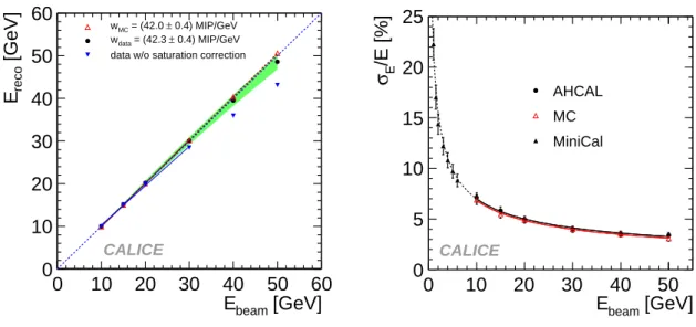
6 Analogue Hadron Calorimeter 23 6.1 Underlying technological principle . . . 23
6.2 Activities so far . . . 23
6.3 Test beam results and operational experience with steel absorber . . . 24
6.3.1 Energy reconstruction . . . 24
6.3.2 Validation of shower simulations . . . 26
6.3.3 Detector performance and stability of response . . . 27
6.4 W-AHCAL test beam results . . . 28
6.4.1 Analysis of the π+/π− data . . . . 29
6.4.2 Analysis of the proton data . . . 31
6.4.3 Calorimeter response and particle types . . . 32
6.4.4 Measurements at the CERN SPS . . . 32
6.5 Steps towards a real detector . . . 33
6.7 T3B - The Time Structure of Hadronic Showers in Tungsten and Steel . . . . 35
7 Tail Catcher and Muon Tracker 36 8 Hadronic calorimeters with gaseous read out 38 8.1 Prototypes based on Resistive Plate Chambers . . . 38
8.1.1 RPC-DHCAL . . . 39
8.1.2 GRPC-SDHCAL . . . 47
8.1.3 RPC technology - Steps towards a real detector . . . 52
8.1.4 RPC Technology - R&D plans . . . 52
8.2 Micromegas for a semi-digital hadron calorimeter . . . 52
8.2.1 Mechanical layout and assembly . . . 53
8.2.2 Large area Micromegas performance . . . 53
8.2.3 Prototype operation, scalability and future plans . . . 54
8.3 Gas Electron Multiplier (GEM) Digital Hadron Calorimeter . . . 56
8.3.1 GEM detector integration with Analog Readout Chip . . . 56
8.3.2 GEM Detector Integration with DCAL . . . 56
8.3.3 GEM Detector Beam Test Preliminary Results . . . 57
8.3.4 GEM Detector and DHCAL Development Plans . . . 58
9 Beam test plans for 2013-2015 58
1
Introduction
The CALICE collaboration was formed in 2001 with the goal to develop and propose options for highly granular calorimeters at future lepton colliders (LC) at the TeV scale. Today, the most advanced proposal for such a machine is the Iinternational Linear Collider, ILC [1], which can operate at centre-of-mass energies between about 0.1 TeV to 1 TeV. In the longer term the Compact LInear Collider, CLIC [2] aims to reach centre-of-mass energies of up to 3 TeV. Even more in the future is the project of a Muon Collider [3].
CALICE is investigating several technological options for both electromagnetic calorime-ters (ECAL) and hadronic calorimecalorime-ters (HCAL), based on the particle flow approach as e.g. introduced in [4].
Within the particle flow paradigm the principal role of the ECAL is to identify photons and measure their energy. The capability to separate photons from each other and from near-by hadrons is of primordial importance. The ECAL forms the first section for hadron showers and with its fine segmentation plays also an important role in the hadron hadron separation.
The role of the hadron calorimeter is to measure the energy associated with neutral hadronic particles, such as neutrons and long living Kaons. In this approach the challenge is to unambiguously identify energy deposits in the calorimeter as belonging to charged particles (and therefore to be ignored) or to neutral particles (and therefore to be measured). As a consequence, the optimal application of PFAs requires calorimeters with the finest possible segmentation of the readout.
Particle flow imposes further requirements on the active element. The calorimeters will be located inside the coil. Therefore the thickness of the active elements needs to be minimised, to keep the coil radius as small as possible. The noise rate needs to be reasonably small, to keep the confusion term manageable. Finally, the active elements need to satisfy general performance criteria, such as reliability, stability, a certain rate capability and be affordable. The CALICE effort involves test beam campaigns with necessarily large installations, and due to the high granularity, some of these have channel counts exceeding those of the largest LHC calorimeter systems. This is only possible by maximizing the use of common infras-tructure such as mechanical devices, electronics architectures and data acquisition systems, and by working within a common software and analysis framework that facilitates combina-tion and comparison of test beam data. Over time, this has allowed CALICE to build up collaborative expertise and to achieve a common understanding of the relative strengths and weaknesses of the technologies under consideration.
The development of calorimeter prototypes is roughly organized in two steps, which in practice may overlap, of course. Firstly, “physics” prototypes provide a proof-of-principle of the viability of a given technology in terms of construction, operation and performance. In addition they are used to collect the large data sets which are invaluable for testing shower simulation programs, and for the development of particle flow reconstruction algorithms with real data. On the other hand, “technological” prototypes address the issues of scaling, integration and cost optimization. They are required for each technology, but many large area and multi-layer issues have initially been addressed with so-called demonstrators, before instrumenting a full volume for larger scale system tests.
The full particle flow performance can only be evaluated in the context of a complete detector design, which is done in the framework of the concept groups ILD [5] and SiD [6]. Also the overall system engineering and integration can only be addressed within a given
concept.
In 2011 CALICE completed a seven year long series of test beam campaigns with physics prototypes of all major ECAL and HCAL technologies. Meanwhile demonstrators are under-going intensive tests for all options, and the commissioning of the first full-size technological prototypes for physics data taking has started.
This comes in time for the preparation of the detailed baseline documents (DBD), de-scribing the detectors together with the ILC technical design report. However, due to the overall unsatisfactory funding situation, all the efforts have not progressed at the same speed, and many beam tests have been carried out so late that the results have not yet been fully extracted. Nevertheless, cross-comparison is possible, and the findings obtained within one technology can often be applied to another.
Distance between shower axes [mm]
0 50 100 150 200 250 300
σ
Probability of recovering within 3
0 0.2 0.4 0.6 0.8 1 10-GeV track CALICE data LHEP QGSP_BERT
CALICE
30-GeV track CALICE data LHEP QGSP_BERTCALICE
Figure 1: Probability to recover the energy of a 10 GeV neutral hadron within three sigma of its true value as a function of the distance from a 10 GeV (circles and continuous lines) or 30 GeV (triangles and dashed lines) charged hadron, respectively. Events are generated by mapping charged hadron showers in the CALICE SiW ECAL, see Sec.3 and AHCAL, see Sec.6, into the ILD calorimeter system, and by reconstructing with PandoraPFA.
One highlight among the rich array of results is the application of a particle flow algorithm to beam test data [7]. Here two displaced showers measured in CALICE prototypes of an analogue hadron calorimeter (AHCAL) and a silicon tungsten electromagnetic calorimeter (SiW ECAL) were mapped into the ILD detector geometry and subsequently processed using PandoraPFA [8] for event reconstruction. Figure1shows the probability to recover the energy of a 10 GeV neutral hadron within three sigma of its true value (where sigma is the detector resolution), as a function of the distance to a 10 GeV or 30 GeV charged pion, compared
with simulations using different physics lists in Geant4 [9]. The good agreement of data and simulations, in particular for the QGSP BERT physics list, underlines the reliability of full detector simulations in predicting the particle flow performance of the detector system.
The evaluation of the basic calorimetric performance and the validation of the simulation models for shower evolution and detector response is concept-independent, and although the technology prototypes are strongly inspired by the ILD and SiD designs, many of the integration issues and their solutions can be generalized.
It is the purpose of this document to present the accumulated knowledge of CALICE for the DBD in a coherent fashion and maximally exploit the possibility for cross-reference, even across the boundaries between concepts. For the common assessment of the status of the technologies, we have defined a set of criteria to be evaluated:
• Established performance: energy resolution, linearity, uniformity, two-particle sep-aration;
• Validated simulation: longitudinal and transverse shower profiles, response, linearity and resolution, both for electrons and hadrons;
• Operational experience: dead channels, noise, stability, monitoring and calibration; • Scalable technology solutions: power and heat reduction, low volume interfaces,
data reduction, mechanical structures, dead spaces, services and supplies;
• Open R&D issues: analysis and R&D to be completed before a first pre/production prototype can be built, cost reduction and industrialization issues.
Although the goal after the LOIs was for full results on all options, due to resource limitations for some issues and technologies the information will not be as complete as might be desirable. Therefore, a consensual assessment of the open issues is essential for the formulation of a coherent R&D program after 2012.
2
Common developments in CALICE
The prototypes are read out by advanced front-end electronics and data acquisition systems. A large number of building blocks of these systems are shared by the prototypes to minimize the amount of specific and parallel development. In case of differences, the coordinated approach within CALICE allows the definition of suitable interfaces between the systems. The offline data management is based on common tools for LC detector R&D to facilitate the integration of beam test results into full detector studies.
2.1 Front end electronics
The CALICE collaboration had to deliver the proof-of-principle that highly granular calorime-ters can be built and that they can meet the requirements for detectors at a future lepton collider. Large scale beam tests have been performed since 2006. In order to avoid confus-ing several effects, the front-end electronics integrated in early prototypes featured a rather conservative design. In a second development stage the particular needs for lepton collider detectors are addressed. This section describes the electronics which have been developed
from the start of the R&D phase until today. It introduces the main features of the applica-tion specific integrated circuits (ASIC). Results on the performance of the ASICs are given in the dedicated sections of the different prototypes.
2.1.1 Front end electronics - ASICs for first large scale beam tests
The ASICs developed and used for the earlier beam test calorimeters were as follows: • FLC PHY3 ASIC [10]: The silicon pads of the physics prototype of the SiW ECAL, see
Sec. 3, are read by an 18-channel ASIC called FLC PHY3. This ASIC, developed in 2002-2003, has been designed in 0.8 µm AMS BiCMOS technology. It provides low noise charge amplification, shaping, and a 12-bit track&hold stage. The analogue multiplexed output is digitized by an external 16-bit ADC. It covers a dynamic range of 14 bits with a noise equivalent of 3500 electrons with the 70 pF detector. The ASIC is linear at the per-mille level. In total, 1000 ASICs were produced at the end of 2003. Beam test campaigns took place at DESY, CERN and FNAL between 2004 and 2011.
• FLC SiPM ASIC [11]: The FLC SiPM ASIC has been developed in AMS 0.8 µm CMOS technology to read out silicon photomultipliers as used in the AHCAL physics prototype, see Sec. 6, and the electromagnetic calorimeter with scintillators (ScECAL) as active material, see Sec. 4. These detectors were tested during beam test campaigns between 2005 and 2011 at DESY, CERN and FNAL. The ASIC re-uses several parts of the ECAL chip FLC PHY3 and is built around a variable gain, low-noise preamplifier followed by a variable peaking-time shaper (20-200 ns), a track&hold, and a multiplexed output. This structure allows single photo-electron spectra with well-separated peaks for absolute calibration at fast shaping (40 ns). It also allows physics signals from the scintillating fibers (up to 2000 photo-electrons) with a slower shaping (150 ns) compatible with the DAQ originally conceived for the physics prototype of the SiW ECAL. In addition, an input DAC allows tuning of the detector gain by varying the operating voltage up to 5 V. The chip accommodates 18 channels, and 1000 ASICs were produced in 2004. More than 8000 channels of SiPM have now been routinely operated since 2006 in test beams at DESY, CERN and FNAL. The overall performance is good. In particular, a photo-electron signal to noise ratio of 4.3 allows calibration spectra showing single photoelectron peaks.
2.1.2 Front end electronics - Towards designs for lepton collider detectors Since 2007, more advanced readout ASICs than those described in the previous section have been under development. These ASICs address several issues crucial for building a detector that can be operated at a future lepton collider. The relevance of the ASIC development for the CALICE prototypes is widely acknowledged and benefits from dedicated funding in Europe by the EUDET program (2006-2010) and the AIDA project (2011-2015) and in the US by the National Science Foundation, NSF. The ASICs described in this section embed all or most of the following aspects:
• Auto trigger, to reduce the data volume;
• Integrated readout sequence and common interface to the 2nd generation data
acquisi-tion system (DAQ) to minimize the number of lines between chips; • Power-pulsing, to reduce the power dissipation by a factor 100. The following ASICs have been designed since 2007:
• HaRDROC [14]: This 64-channel chip provides a semi-digital readout with three thresh-olds tunable from 10 fC up to 10 pC and integrates a 128-deep digital memory to store the 2 × 64 discriminator outputs and bunch crossing identification. HaRDROC is the first ASIC for which large scale power-pulsing was tested at system level, allowing a power reduction by a factor 100 while keeping the detector efficiency above 95% [15]. 10,000 ASICs were produced in March 2010 to equip the 40-layer, cubic meter proto-type of the glass RPC semi-digital hadron calorimeter (GRPC-SDHCAL), as detailed Sec. 8.1.2.
• MICROROC [16]: This 64-channel ASIC is very similar to HaRDROC, except for the very low noise input front end (0.2 fC), which allows the detection of signals down to 1 fC. It also ensures robustness against remnants of mesh sparks. A total of 1000 ASICs were packaged in 2011 and 2012 to equip four MicroMegas chambers, each of one square meter area, see Sec. 8.2, which were exposed to beam tests in 2012.
• SPIROC [17]: This ASIC is designed to read out the silicon photomultipliers used in the second prototype of the AHCAL, see Sec. 6 and in the ScECAL, see Sec. 4. SPIROC is an evolution of the FLC SiPM ASIC and contains 36 auto-triggered, bi-gain, power-pulsed channels. Each channel can measure and digitize the charge over 12 bits from 1 to 2000 photoelectrons, and measure the time with a TDC that is accurate to 1 ns. An ultra-low power 8-bit DAC has been added at the preamplifier input to tune the input DC voltage and therefore to adjust the SiPM high voltage individually. Since 2010, SPIROC ASICs have being operated at system level with good preliminary results. First tests of the TDC ramps indicate that a resolution better than 1 ns can be achieved. Power-pulsing tests at system level have just begun. The KLAUS ASIC [18] is a derivative of the SPIROC ASIC, featuring a low noise architecture. Recent results demonstrate a signal-to-noise ratio better than 10, for a signal charge of 40 fC. The front end used in the KLAUS ASIC is therefore another good candidate to replace the analogue front-end circuit in the next version of the SPIROC ASIC, SPIROC2.
• SKIROC [19] is designed to readout the silicon pin diodes of the second SiW ECAL prototype, see Sec. 3. This 64-channel ASIC is a derivative of the FLC PHY ASIC. It also keeps most of the analogue part of SPIROC2, except for the preamplifier (a low noise charge preamplifier). It is followed by a low gain and a high gain slow shaper in order to handle a large dynamic range from 2 fC up to 10 pC.
• DCAL3 ASIC [20]: This ASIC reads out the prototype of the digital hadron calorimeter (DHCAL) based on resistive plate chambers which is detailed in Sec. 8.1.1. This per-forms all of the front-end processing and also has ancillary control functions. DCAL3 implements signal amplification, discrimination/comparison against threshold, record-ing the time of the hit, temporary storage of data and data readout. Each chip contains 64 detector channels and each channel has two programmable gain ranges (10 fC and 100 fC sensitivity). When charge is received by the front-end amplifier and exceeds a
programmable threshold (common to all channels in the chip), the hit pattern of all channels in the chip is recorded along with the time. The timing of hits in the DCAL3 chip is implemented using the concept of a “timestamp” counter. This counter is reset once per second across the system, and advances with each 100 ns clock, which is also synchronous across the system. When triggered, either from an external trigger or self-triggered, the data is captured in a readout buffer inside the chip. Data are read from the chip using high-speed serial bit transmission. The ASIC also has slow control func-tions, on-board charge injection, and the ability to mask off noisy channels. CALICE is now considering the development of the next generation readout system. Discussions on the design of a new front-end ASIC have focused on: a) lower power consumption, b) token ring passing, c) redundancy and reliability, and d) increased channel count. All these ASICs were produced in 2010 to equip large scale detectors and to check that all key issues had been solved during the 2010-2012 beam test campaigns. The next R&D step within CALICE includes designs in which all channels are handled separately to allow higher zero-suppression. This is a major modification, especially for the digital parts, as it implies a complex management of the readout. Furthermore, an I2C link with triple majority logic for radiation tolerance will be integrated into the ASICs.
In addition, other R&D studies have been underway since 2003 by several microelectronics groups within the CALICE collaboration to evaluate alternative front end architectures and also low power, high resolution ADCs (cyclic and pipeline ADCs) [21,22].
2.2 Data acquisition systems in CALICE
The majority of the results presented in this note were obtained with detectors read out by the data acquisition which is described in detail in [23] and is outlined in the following.
The off-detector electronics distributed the sample&hold signal, required by the very front-end (VFE) electronics within a latency of 180 ns and with an uncertainty of less than 10 ns to provide the digital sequencing necessary to multiplex the analogue signals from the VFE, to digitize the signals and to store the data. The analogue signals have a 13-bit dynamic range, and the electronics is required not to contribute significantly to the analogue noise. Assuming a standard beam test spill structure, the target for the electronics is to run at an event rate of 1 kHz during the beam spill, with an overall average rate of 100 Hz.
The calorimeter readout is based on the “CALICE Readout Cards” (CRC) [24]. These are custom-designed, 9U VME boards derived from the Compact Muon Solenoid tracker Front End Driver readout boards [25] but with major modifications to the readout and digitization sections.
Each CRC consists of eight front-end (FE) sections feeding into a single back-end (BE) which provides the interface to VME. The whole board is clocked from an on-board 40 MHz oscillator.
The complete system performed well in the beam test environment. The sample & hold is distributed on the derived 160 MHz clock within a minimum of 160 ns, allowing the rest of the latency of 180 ns to be implemented as a software-specifiable delay in the FE FPGA. The CRC noise when detectors were disconnected is very low, with an average of 1.4 ADC counts, compared to e.g. around 5.9 ADC counts from the ECAL VFE electronics
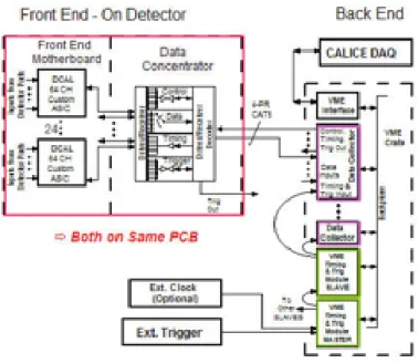
Figure 2: Block diagram of the DHCAL read out system. See text for details. 2.2.1 DHCAL DAQ system
A block diagram of the system is shown in Fig.2. The electronics is divided into two groups. The “front end” (on detector) electronics processes charge signals from the detector, collects data for transmission off detector, and acts as the interface for slow controls. The “back end” electronics receives and processes the streams of data from the front-end electronics, and in turn passes it to the DAQ system. It also has an interface to the timing and trigger systems. The output data streams from the DCAL3 chips in the front-end are point-to-point serial LVDS, sending data to the data concentrator (DCON) field programmable gate array (FPGA) that resides on the outer edge of the front end board (see Sec.8.1.1for details). Each data stream is received by a FIFO in the data concentrator. A state machine in the FPGA cycles through the 24 FIFOs, and selects the data that has the lowest timestamp. This data is written out first, followed by the next smallest timestamp, etc. In this way, the data coming out of the data concentrator is time-ordered. When using an external trigger, all chips respond at the same time with the same timestamp. The data is read out serially from the front-end boards, using “data push”, into custom 6U VME cards in the back-end system called data collectors (DCOL). The DCON also fans out the clock and trigger signals that are received from the DCOL. The data is time-sorted using the timestamps, and stored in readout buffers. The data is read periodically into a computer, where higher-level algorithms perform the triggering and event reconstruction. The DCOLs also provide an interface to the front-ends for slow control communication and timing. The VME crate that hosts the DCOL also contains a module that receives timing and trigger signals from peripheral subsystems, and communicates with the DCOLs to provide this information to the front-ends. Each DCOL services 12 front end boards using bidirectional serial communication links over CAT5. There is one link per front end board. Two pairs in each link are used for bidirectional communications. Each pair carries an LVDS serial bit stream with a basic clock rate of 40 MHz. In addition, a dedicated asynchronous isolated signal is provided to the
front-end for test pulse synchronization. The links incorporate both DC and AC isolation up to several hundred MHz by means of a capacitive digital isolator, with power delivered from the DCOL via an additional cable pair. The DAQ hardware for the DHCAL consisted of two CAEN V2718 VME controllers and a A2818 PCI adapter mounted in a SuperMicro 5035B-T Workstation running Scientific Linux 5. The two VME controllers, connected in a daisy chain configuration, were read out by a 20 m optical fiber connected to the PCI adapter. The driver software and C language interface library supplied by the hardware vendor were used along with the Hardware Access Library (HAL) software library [27]. The DHCAL DAQ software was based on a modular system [26] written in C++ originally developed to support the CALICE Readout Card (CRC) that we extended to support the DHCAL electronics. This system has been used by several other detector prototype projects in the collaboration. Software modules tailored to the specific needs of the DHCAL front-end and back-end electronics were deployed in both DHCAL standalone operations, such as cosmic ray tests, as well as in beam tests along with other detectors using the CRC. In most of the beam tests a network of three computers was used, one for the DHCAL readout, one for the trigger and CRC readout, and one to record the data. The system was designed so that it could be scalable. In Fig.2, two VME back-end crates are shown. In many of the tests that have been done to date, only one VME crate was used.
2.2.2 Data acquisition system emerging from the EUDET project
CALICE and the EUDET project [28] together developed a generic data acquisition system which was used by all prototypes of the CALICE collaboration brought into operation after the year 2010. These prototypes feature embedded, auto-triggered readout ASICs, Sec.2.1, equipped with local storage and allow for power pulsing. These are requirements for calorime-ters at an ILC-like accelerator.
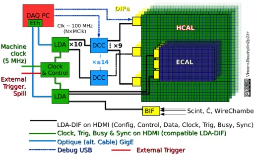
The DAQ has been designed to be generic and scalable [29,30]. It consists of 4 parts as illustrated in Fig.3. From the detector outwards these are: the detector interFace (DIF) cards are detector specific and provide control of the ASICs of a detector. Their external interface consists of a single HDMI cable carrying the data in and out, bringing the clock and trigger and collecting the BUSY signal out, all on differential pairs; a single local data aggregator (LDA), or double level of data concentrator cards (DCC) and LDAs, connect the DIFs to the clock and control card (CCC), centrally managing the fast signals (clock and trigger) and the sequencing (acquisition operations), based on the BUSY signals from the DIFs and external signals, and to a PC through a gigabit Ethernet connection (for configurations loading and data readout).
Despite heavy laboratory stress-testing on small set-ups, these cards proved fragile (me-chanically and electrically) in experimental hall conditions when used on a large prototype (the GRPC-SDHCAL cubic metre detector, with 0.4 M channels and 150 DIFs) during a test beam in summer 2011 at CERN. For a small setup (6 DIFs reading out ECAL sensors) the same system worked smoothly during summer 2012 at DESY.
Meanwhile an intermediate solution was designed for the GRPC-SDHCAL and was suc-cessfully used during several test beam campaigns in 2012. Using the same hardware but diverting the data path of the DIFs through USB cables, a smooth operation was possible at the cost of a limited data rate (∼ 20 Hz of trigger during a spill, where a trigger includes several events stored in the ASIC memory).
Figure 3: Layout of the second generation DAQ system. See text for details.
rewritten, ensures the interface to the DAQ hardware. The high level functionality for read-out and control is based on the XDAQ framework (used for the CMS tracker system). It allows for a flexible architecture of task sharing on multiple computers, online treatment and monitoring. The configuration is dynamically generated from an Oracle database, while the run conditions are stored in an sqlite database. The data is written in RAW LCIO format [31] and stored on the GRID.
To circumvent some limitations of the LDA (essentially designed as a prototype of the ILD DAQ), a surrogate (called GigaDCC) is being developed: it should serve the dual purpose of being flexible for test beam operation and will provide experience for an large DAQ system for the ILC. This equipment will also be used by the forward calorimeter (FCAL) test-bench and a geological volcano survey at Clermont-Ferrant. In addition, a new custom-sized LDA board, which fits into the AHCAL cable shaft of the ILD version, is being developed. This board has a very short connection to each single DIF and avoids the large cable tree of an LDA board placed on top of the calorimeter. A prototype will be used in a beam test in spring 2013.
The CCC cards are also being redesigned to allow for better mechanics, improved logical capacities and better input/output handling. The first pre-prototype was successfully used in beam tests with SiW ECAL ASUs in March and July 2012. The new CCC cards will also allow for an interface to the EUDAQ HW (clock, trigger, BUSY and event number sharing), defined in the framework of AIDA [32]. This is in the context of performing combined tracker and calorimeter test beam within 3-4 years from now. This also serves as a testbench for a global acquisition system for the ILC.
2.2.3 Operation modes
Four modes of operation are foreseeable in testbeam:
1. An ILC mode in which the ASICs are put into acquisition at the start of a spill (ILC or beam test facility) and read out at the end of spill or when any of the chips send a
full signal;
2. a mixed-triggered mode using the ASIC auto-trigger features and an external signal to start the readout. On full, all chips must be reset;
3. a standard mode using an external signal to trigger the ASIC acquisition and imme-diate readout (no auto-trigger);
4. a delayed-triggered mode in which the data acquired in auto-trigger mode is only kept if an external validation signal is received within a given time window.
In each case here the external signal can be a logical combination of a hodoscope signal or a simple clock. The choice of the running mode depends on the size of the chip memory and noise frequency vs. physics rate in the detector. The ILC mode and mixed-triggered mode have been extensively tested in the laboratory for the GRPC-SDHCAL and the SiW ECAL prototypes. They are both prone to noise sensitivity; a very fine monitoring of the detector should be performed constantly and immediate action (masking, gain reduction) taken and recorded for later analysis. The other two operation modes are still to be tested.
2.3 CALICE computing
From the beginning, the computing infrastructure of the CALICE collaboration has been based on tools common to the LC activities [33, 34]. The software uses LCIO as the data format and at an early stage of reconstruction applies objects like LCCalorimeterHits which are part of the LC data model. Embedding of low level (i.e. close-to-hardware) models into LCIO is likely within the next few years. Here again CALICE is expected to play a prominent role. From the very beginning CALICE also used grid tools for data management and processing. It should be noted that CALICE has so far collected around 20 TByte of data. The virtual organization (VO) calice was established in 2005 and so far has around 80 members. It is hosted by DESY but benefits from support from around 20 computer centers in Asia, North-America and Europe.
2.4 Organisation of beam test campaigns
Beam test campaigns are always prepared within the CALICE Technical Board. So-called Major Beam Tests have been accompanied by dedicated proposals or Memoranda Of Un-derstanding and presentations in front of panels of the corresponding institutes [35,36,37]. Major beam tests have been conducted at CERN and Fermilab. This coordinated approach resulted in CALICE gaining a good reputation at the corresponding sites. If the LC efforts converge towards the formation of detector collaborations, these collaborations will surely benefit from these established contacts at the beam test sites. For these beam tests, an elec-tronic logbook as well as remote conferencing have been set up [38]. These tools significantly facilitated communication during the beam tests and allowed participation from remote sites. These tools should be preserved and extended for any future activity.
3
Electromagnetic calorimeter with silicon
For use as a particle flow detector, the ECAL must have excellent two-particle separation (down to distances of a few cm) and a reasonably good single photon energy resolution,
not worse than around 20%/pE[GeV]. Two-particle separation is achieved by a highly segmented readout together with a minimisation of size of electromagnetic (EM) showers. A sampling calorimeter with tungsten absorber and thin, highly segmented sampling layers can provide such performance. The small Moli`ere radius and radiation length of tungsten give compact EM showers, while its relatively long hadronic interaction length also gives some natural separation between EM and hadronic showers. The sampling layers must have a small thickness (to reduce the overall Moli`ere radius) and be easily segmented (at the level of 5 mm) in order to give the necessary readout granularity. These requirements can be satisfied by silicon sensors. Matrices of PIN diodes made in ∼ 300 − 500 µm-thick high resistivity silicon, typically 5 kΩ · cm, can be fully depleted by the application of a modest reverse bias voltage (100-200 V), giving a sensor which is also rather stable and insensitive to environmental conditions. The proposed technology is supposed to assure an excellent signal over noise ratio. This excellent signal over noise will also provide sensitivity to small energy depositions, thus facilitating the two particle separation. The R&D goal for the signal over noise ratio is 10:1.
3.1 Detector prototypes
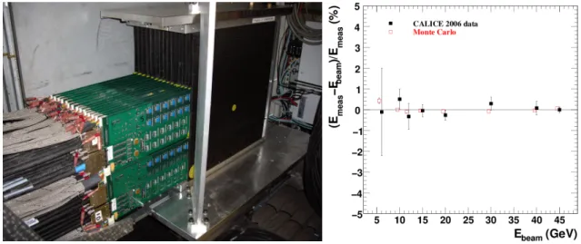
The CALICE SiW ECAL group has developed a first so-called “physics prototype [23], shown in Fig,4, whose aim was to demonstrate the ability of such an ECAL to meet the performance requirements. It had an active area of 18 × 18 cm2 and 30 sampling layers. The active sensors
had a granularity of 1 × 1 cm2, giving a total of nearly 10 k readout channels.
A second, “technological” prototype is presently under development [44]. This prototype is used to develop and test the technologies required to integrate an ECAL into a larger detector, and to prepare for the eventual construction of a full detector, including aspects of industrialisation.
3.2 Elements of the R&D and main conclusions
The SiW ECAL physics prototype has successfully and stably operated between 2004 and 2011. No major systematic problems were identified with the concept of this detector or with its technical design. For the physics prototype the signal over noise ratio was determined to be 7.5:1, which is remarkable for the early stage of the R&D at which the physics prototype was constructed.
The stability of the detector is well demonstrated by the results of the periodic calibrations of all detector channels (typically two calibrations per test beam period). The calibration factors found were stable over long time periods to the % level, and showed no influence from external factors.
The response of the detector to electrons is presented in [39]. The energy response is found to be linear to within 1% in the energy range between 1 and 45 GeV, as shown in Figure 4. The energy resolution for electrons was measured to be 16.6/pE[GeV] ⊕ 1.1%.
Both the energy response and the longitudinal shower profiles of electron showers are well described in the simulation, as is the effective Moli`ere radius.
The studies by the CALICE collaboration presented in [40] and [41] confirm that the basic cross sections for hadrons are well implemented in the simulation toolkit. The lateral shower extension which is relevant for the overlap of hadron showers and thus for their separation has been studied in detail. Figure 5 shows in its left part the shower radius for energies
Figure 4: Left: The SiW Ecal physics prototype detector. Right: Residuals from a linear response for both, data and simulation.
between 8 GeV and 80 GeV. This study has been extended to energies as small as 2 GeV. An example is shown in the right part of Fig.5.
The high granularity of the calorimeter allows the tracking of particles as they pass through the detector and the use of imaging processing techniques. For instance, the Hough transform technique has been tested to find tracks in the calorimeter [42]. This technique has been applied to reconstruct a muon track near to a 30 GeV electromagnetic shower. Figure6
shows the reconstruction efficiency as a function of the distance between the track and the shower axis. The efficiency reaches 100% from a distance of 25 mm.
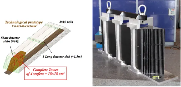
Figure7 shows a schematic view of the technological prototype: The mechanical housing is realised by a tungsten-carbon reinforced epoxy (CRP) composite, which supports at the same time the absorption medium and ensures the mechanical integrity of the detector. The mechanical structure must be sufficiently strong and rigid to hold the massive absorber, while having rather precise dimensions and a minimum of insensitive areas.
The manufacture of mechanical structures in carbon fibre composite materials is well understood, and a large prototype structure, close in scale to a barrel module for ILD, has been produced, see the left part of Fig.8. This exercise was very successful. A deviation from planarity on the top and bottom side of the structure of about 5 mm was measured. This bending would be tolerable for a module for a full detector. However, the assembly procedure will be revised in order to achieve an even better planarity of the structure.
Work is also progressing on the end-cap structures, where longer structures are required and the orientation of modules is different to those in the barrel. The design of the end-caps presents some difficulties, since the weight of the tungsten exerts a shear force on the horizontal alveolar structures, to which the present module design is not particularly resistant. Studies are continuing to understand if a modest modification of the design can give the required strength, or if a more radical redesign is required.
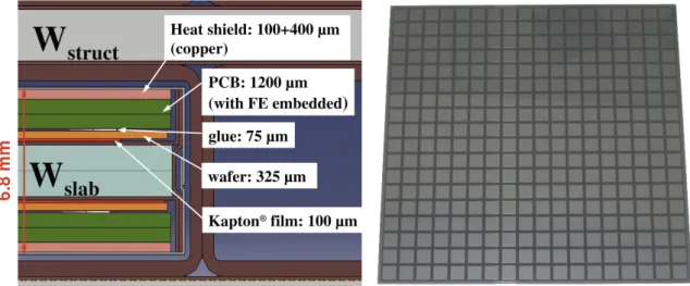
The left part of Fig. 8 shows a cross section through two calorimeter layers which form a slab. The sensitive parts will be mounted on two sides of tungsten board and inserted into the alveoli of the mechanical structure. A slab will have a height of about 6.8 mm, which is to be compared to the height of one alveolar of 7.4 mm.
Figure 5: Left: Comparison between data and simulation of the lateral shower profile for energies between 8 and 80 GeV. Right: Shower radius at 2 GeV. Data are compared with the prediction of the QGSP BERT physics list. The bottom view shows the ratio of simulation and data.
The silicon sensors are the central component of the detector, and also the most expensive. Work is progressing on the improvement of the sensor design, particularly of the sensor edge. Silicon sensors of various designs have been purchased. These include large 9 × 9 cm2 sensors
from Hamamatsu Photonics as shown in the right part of Fig. 8. The Hamamatsu sensors have excellent electrical characteristics, and a number of them have been successfully tested in beam tests. An undesirable feature was identified in beam tests with the physics prototype. A cross-talk was observed between the (electrically floating) sensor guard rings and the pixels at the sensor edge. When a large energy was deposited in the guard ring (or an edge pixel), such cross-talk could give rise to cases where all pixels at the sensor edge recorded a signal, provoking so-called “square” events. Tests with small sensors with segmented guard rings have demonstrated that such a design can indeed mitigate the transmission of signals along the sensor edge [43]. An attenuation up to a factor of 80 was observed. The already mentioned samples from Hamamatsu feature therefore designs with various edge widths and guard ring layouts as well as smaller sensors with segmented guard rings and using edgeless technology. An equally important aspect is the understanding of the eventual sensor cost, and to develop strategies to reduce it. Simpler and/or “open” designs, which could then be manu-factured by non-specialist companies, are also under development.
Development of the PCB which carries the silicon sensors and SKIROC ASIC has been somewhat problematic, due to the rather thin board required (no thicker than 1.2 mm), together with its rather large area. This has given rise to problems with the planarity of prototypes received so far. At present PCBs with a relaxed thickness constraint and using packaged ASICs have been produced and are functional. PCBs with wire bonded unpackaged ASICs incorporated into the PCB volume have already been produced, again with relaxed thickness constraints. Further developments are required to produce sufficiently thin and flat PCBs with encapsulated unpackaged ASICs. Developments for the technological prototype have demonstrated that the placing of the front end electronics within the detector does not induce significant spurious signals when the ASIC is placed in the maximum of a high energy
distance MIP shower axis [mm] 0 10 20 30 40 50 60 Ε detection efficiency 0 0.2 0.4 0.6 0.8 1 CALICE preliminary
Figure 6: Efficiency of MIP detection as a function of distance from an electron shower.
Figure 7: Left: Schematic view of the technological prototype with dimensions. Right: Me-chanical structure of the technical prototype.
electron shower [46].
A calorimeter layer will have a length of about 1.5 m in the barrel and up to 2.5 m in the end-caps and will be composed of several units which carry the sensitive devices as well as the front end electronics. The devices are called Active Signal Units or ASUs. Great care is taken in the development of the technique to interconnect the ASUs. Apart from the reliability of the signal transfer along the slab the interconnection must not exert mechanical or thermal stress e.g. to the silicon wafers which are very close to the interconnection pads. Good progress has been made in the past years and a viable solution is currently applied to the first layers of the technological prototype of the silicon tungsten Ecal. The fragile ensemble has to be inserted into the alveolar structure which houses the calorimeter layers. The integration cradles are under development and a first integration test with a demonstrator has been successfully conducted. For this demonstrator a cooling system has been developed,
Figure 8: Left: Cross section through one slab of the prototype with the thickness of the various components. Right: Hamamatsu Photonics silicon sensor: 324 pixels of5 × 5 mm2.
which in an upgraded form is already available for the large scale prototype [45]. This cooling system, which is also already conceived in view of a final detector, is a leak-less water system. A heat exchanger will be coupled to a copper drain at the outer part of the Ecal layers. This outer part will be equipped with the interface card to the DAQ system and the FPGA mounted onto the interface card may be a ’hot spot’. The copper drain assures the heat evacuation of residual heat from the inner parts of the detector layers. The R&D studies have led to the result that the temperature gradient along an Ecal layer is about 6◦C in
the detector end-caps and only 2.2◦C in the barrel region. Due to this comparatively small temperature gradient the concept of applying cooling only at the detector extremity seems to be appropriate.
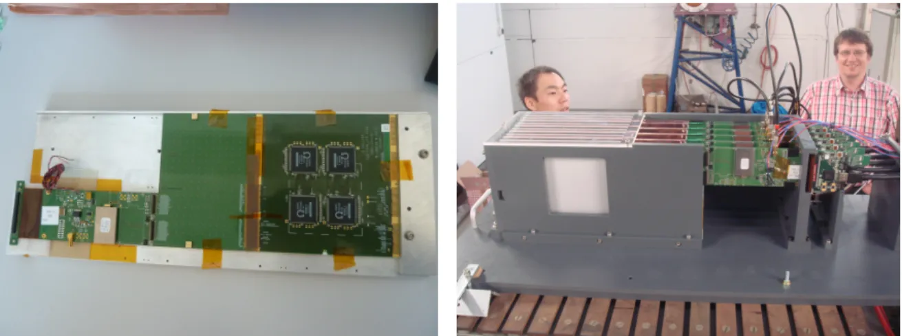
Beam tests with a number of short layers equipped on only one side of the tungsten plate of the “technological” prototype have been performed in spring and summer 2012, see Fig. 9. The system tested in summer comprised six wafers distributed over six ASUs. The whole detection chain, from the sensor, ASIC, PCB, interface card to the DAQ system were tested for a total of 1200 calorimetric cells. A calibration chain has been established and the preliminary analysis of the data indicates that the signal over noise ratio is better than that of the physics prototype. The successful tests in 2012 allow for the conclusion that the system can be extended to a larger scale prototype of up to 45000 cells. Note that these tests are a prerequisite to address now crucial system aspects such as power pulsing of the front end electronics.
3.3 R&D plans and steps towards a real detector
The concept based on silicon has been proven to be a suitable choice for an electromagnetic calorimeter for the particle flow approach. The next few years will be used to progressively complete the technological prototype with up to 30 short ASUs and at least one long layer. The realisation of this prototype will be used to test several different technical solutions for various aspects of the detector construction.
Figure 9: Left: Picture of one layer of the SiW Ecal setup tested in 2012. Right: Experimental setup at DESY.
wafer read out by four SKIROC ASIC. The very next step is to produce ASUs with four wafers on, which would then be read out by 16 ASICs. PCBs with the final design have been ordered in summer 2012 and are available now. The final layout of the calorimeter for a linear collider detector depends significantly on the success of the PCB manufacturing. It can not be excluded that the PCBs are also a sizable cost driver of a final detector. Further development of the front end PCBs is required in order to satisfy the requirements on thickness, planarity and number of readout channels using unpackaged, encapsulated ASICs. As for the sensors a close collaboration with industrial partners is needed. An alternative based on ultra-thin BGA packaging of the ASICs is under study.
Detector slabs for ILD will be up to ∼ 2.5 m in length. We plan to make the first long slab to test that such a long device, with its 10000 readout channels, can be successfully read out using a single DAQ interface at one end of the slab. Given the tight financial situation the first test will encompass equipped layers at both extremities of the layer. It is however expected that these studies will allow already to judge whether these long slabs and readout chains, can be realised in a reliable way.
The silicon sensors are a major cost driver for the ECAL (which represents a significant fraction of the total ILD cost). Discussions have started with HPK on developing an under-standing of the cost drivers for sensor production, and we have a first (unofficial) cost estimate for an eventual large-scale production. A larger number of silicon detector manufacturers will be used when a full ECAL is built, preferably some rather “generic” silicon producers, rather than silicon detector manufacturers. Such “generic” producers are generally more hesitant to perform an R&D program without the real prospect of a full detector production.
Once a firm estimate of the sensor cost is available (probably not before the decision to build a linear collider), a cost-performance optimisation will need to be performed. If the cost of the ECAL as presently envisaged is prohibitively high, it may be necessary to consider an ECAL with a smaller number of sampling layers (and therefore smaller total silicon area), of smaller inner radius, or a hybrid design with a combination of layers of silicon sensors and of a less expensive technology, for example scintillator strips with silicon photomultiplier readout. Simulation studies of such detector configurations are underway. Further development of links with silicon sensor manufacturers is essential in order to better understand the eventual cost
of such a detector, and to prepare for possible mass production. The use of power pulsing in the front end electronics is a central tenet of the detector design, and a series of detailed tests of this technology must be performed to develop sufficient confidence in this technique. This will include tests of both rather large power pulsed systems and probably smaller systems inside a magnetic field. The two latter tests are envisaged for winter 2012/13.
Many steps of detector construction will be outsourced to industry, and one aim of the technological prototype is to choose techniques which are well adapted to an industrial pro-cess. In parallel with this, a significant quality control control process will have to be devel-oped, with tests of detector components being carried out at various stages of their integration into detector elements.
4
Electromagnetic calorimeter with scintillator
4.1 Idea of technology
The required ECAL granularity for PFA, roughly 5 × 5 mm2 lateral segmentation, was
un-til recently difficult for the scinun-tillator technique, because a sufficiently small and sensitive readout technology did not exist. The situation was drastically changed when the pixelated photon detector (PPD) was developed. Each small segmented plastic scintillator can be directly read out by a PPD without a large dead volume coming from the readout. The scintillator-tungsten electromagnetic calorimeter (ScECAL) is a unique concept using such a technique. Like the SiW ECAL, it is a sampling calorimeter with 2–3 mm thick tungsten plates interleaved with 20–30 of sensor layers. In order to increase the feasibility of such a calorimeter and to prevent dead volume from PPDs, it is proposed that each scintillator is shaped as a 45 mm × 5 mm strip, with the scintillator strips in odd layers orthogonal to those in the even layers [5]. This strip scintillator technique has the potential to drastically reduce the cost of a detector like ILD. Figure 10 shows the structure of such a scintillator strip ECAL (ScECAL).
Figure 10: Schematic of the structure of the ScECAL. Top scintillators (pink) are parallel to the plane of this figure, while the scintillators at the bottom are perpen-dicular to the plane.
Energy of One Jet (GeV)
0 50 100 150 200 250 300 RMS90/E (%) 0 1 2 3 4 5 6 7 8 9 10
45mm Si strip w/o SSA 45mm Si strip w/ SSA SiECAL Default (5mm) SiECAL in LOI
Figure 11: With the strip splitting algo-rithm (SSA), strip ECAL shows similar performance (blue) to the 5 mm × 5 mm SiECAL (open circle), while it degrades without SSA as the jet energy increases (red).
To extract an effective 5 × 5 mm2 lateral granularity from 45 × 5 mm2 strip cells a special
algorithm, Strip Splitting Algorithm (SSA), has been developed [52]. Figure 11 shows the energy dependence of the jet energy resolution of two-jet events according to Monte Carlo simulation. To focus on the performance of the SSA algorithm, the strips are made of silicon and the layer structure is the same as the SiECAL in the MC simulation, so that we can use the same tuning parameters of PFA as for the normal SiECAL. With the use of SSA, the 45 mm strip SiECAL and the conventional SiECAL give similar performance of jet energy resolution for 45 GeV jets and 100 GeV jets. For the high energy jets, a study to put 5 × 5 mm2 cell layers in between strip layers is ongoing. This configuration is expected
to solve the two-fold ambiguity. In this so-called “hybrid” configuration the Si-ECAL layers described earlier could be employed as the square cell layers.
4.2 Activities
The ScECAL group has developed the physics prototypes in two steps, 1) 24 layers of 3 mm thick scintillators of 90 × 90 mm2 lateral size were tested at DESY in 2007 and 2) 30 layers
of 3 mm thick scintillators of 180 × 180 mm2 lateral size were tested at FNAL in 2008 and
2009. Both modules have the same tungsten absorber plates in between sensitive layers and the thickness of 3.5 mm with 30 absorber layers leads to a total radiation length of 21.3 X0. From the results of the first module and a small test beam at KEK in early
2008, the adapted design of the scintillator-PPD unit for the second physics prototype is: 1) the scintillator strip is hermetically enveloped with a reflector film has a width, length, and thickness of 10 mm, 45 mm, and 3 mm, made by using an extrusion method developed by KNU. 2) the scintillation photons are collected by a wavelength shifting (WLS) fiber, inserted centrally, along the longitudinal direction of each strip and read out with a PPD provided by Hamamatsu Photonics KK, “1600-pixel MPPC [53]. 3) the protruding area of a square-shaped sensitive area of PPD from the round-square-shaped cross-section of WLS fiber is covered by a reflector film to reject photons which come directly from the scintillator. This design of the scintillator-PPD units show good uniformity of the position dependence of response and a sufficient number of p.e. for mip-like events (average > 15 p.e.).
With the second prototype module, this calorimeter concept has been tested in September 2008 and May 2009. The second prototype also included an LED gain monitoring system for each channel. Round holes are made in the reflector film above each channel in order to introduce LED light into the scintillators, as seen in Figure12. The test beam experiments were performed at the MT6 experimental area in the Meson Test Beam Facility (MTBF) of FNAL. The first generation front-end electronics based on the FLC-SiPM ASIC for the AHCAL has also been employed for the ScECAL. The data taking conditions are: 1) 32 GeV muons for the calibration, 2) 1 - 32 GeV electron beams to study the linearity of response and the energy resolution, 3) 1- 32 GeV electron beams and 2 - 32 GeV pion beams with tilted incident angle toward the detector to see the effects of incident angle, 4) 2- 32 GeV neutral pion beams created 1800 mm in front of the detector face to study the reconstrucion of two-photon events. Analyses of these data are ongoing.
4.3 Main conclusions
The left part of Figure 13 shows the energy response reconstructed from the electron beam data of 2 - 32 GeV taken in May 2009. The response of each channel has been corrected for the effects of PPD saturation. Temperature corrections are established using the relation between
Figure 12: A layer of physics prototype and scintillator PPD unit. a. 1600 pixel MPPC, b. scintillator made with the extrusion method, c. WLS fiber.
ADC/MIP conversion factor and temperature of detector and also between ADC/photon conversion factor and the temperature. Applying these corrections the ScECAL prototype shows stable response with a large temperature fluctuation between 19 - 28◦C, such that the
deviation from linear behaviour is less than 2%.
The right part of Figure 13 shows the intrinsic energy resolution of the prototype. The stochastic term is 12.9±0.1(stat.)±0.4(syst.)%, and the constant term is 1.2±0.1(stat.)+0.4−1.2(syst.)% where the intrinsic momentum spread of the beam is subtracted from each ECAL data.
With three major test beam experiments, the ScECAL physics prototype has shown better performance than that required for ILC physics in terms of its linearity of response and energy resolution in the range from 2 to 32 GeV.
4.4 Steps towards a real detector
After the physics prototype, 5 × 5 mm2 lateral granularity is required to get better
perfor-mance of PFA. Therefore, the technology of 5 mm width scintillators directly coupled to a PPD needs to be established.
The same concept of the alveolar structure as the SiECAL, see Section3, is also employed for ScECAL: a pair of sensor layers on either side of a tungsten absorber plate is inserted into an alveolus, where each sensor layer is read out via a printed circuit board (PCB). The PCB with ASIC architecture and DAQ system is being developed with strong support by collaborating with SiECAL group and AHCAL group. Details are in the following subsections. 4.4.1 Scintillator/PPD unit
As the scintillator width is reduced to be 5 mm, the direct coupling of PPD to the scintillator is required to reduce the dead volume coming from the WLS fiber. A uniform response has been almost achieved, although a final optimization of the coupling of scintillator and PPD is still to be finished. In order to achieve automatic mounting of ∼ 107 PPDs and scintillators
D e p o s it e n e rg y i n E C A L ( M IP ) 0 500 1000 1500 2000 2500 3000 3500 4000 4500 CALICE preliminary
Beam momentum ( GeV/c )
0 5 10 15 20 25 30 35 Deviation (%) #: # -4 -2 0 2 4 ) GeV/c ( 1/ beam p 1/ 0 0.1 0.2 0.3 0.4 0.5 0.6 0.7 0.8 (%) E / E σ 0 2 4 6 8 10 12 CALICE preliminary
Figure 13: Left: Linear response of the physics prototype of ScECAL (top), with the deviation from the result of linear fit, which is less than 2%. Right: Energy resolution of the physics prototype of ScECAL where the intrinsic momentum spread of the beam is subtracted from each ECAL data.
The saturation property of PPD is moderated by increasing the number of pixels. Large pixel number MPPCs are being developed with Hamamatsu Photonics and a 4400 pixel MPPC has already been achieved, while 1600 pixel MPPCs have been used for the physics prototype. The properties of such new devices are being measured.
4.4.2 Sensor layer on printed circuit board
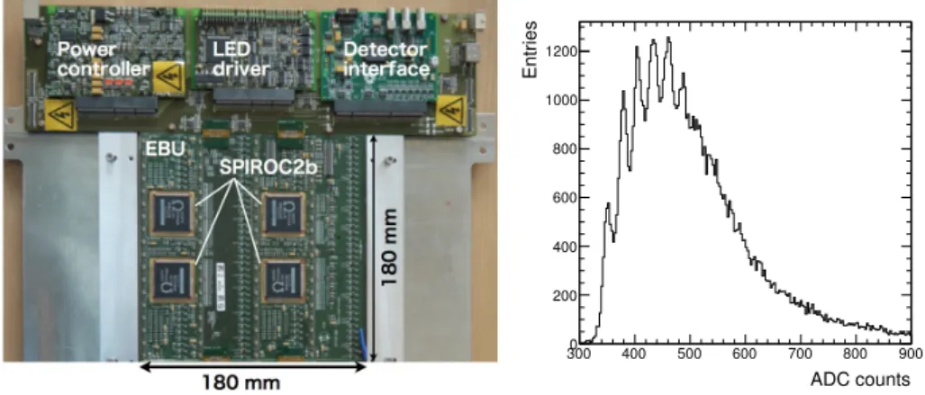
The printed circuit board for ScECAL, called “EBU” is being developed with the technology for AHCAL. Four rows of 36 scintillator strips are embedded on a EBU controlled with four ASICs, called SPIROC2b as shown in the left part of Figure 14. The first version of “the technological prototype of ScECAL” to test the feasibility of the technology with one EBU has been commissioned with electron beams at DESY in October 2012. The right part of Figure 14 shows an energy spectrum of mip-like events for a channel clearly showing the photo electron peaks separated by using MPPCs.
The EBU has also the timing measurement functionality for the requirements of ILC physics. Although the necessity of the power pulsing is not yet discussed for ScECAL, EBU already implements power pulsing functionality.
To realize the detector construction of ∼ 107channels, automatic integration of ingredients
including scintillator/PPD units on EBU is developing.
4.5 R&D plans
In order to develop and test the technologies required to integrate ScECAL into the real detector, the technological prototype of ScECAL is being further developed.
The current technological prototype is not enough to be ready for integration into the real ILD. For example, thickness of EBU is required to be reduced less than 1 mm. To reduce the thickness of EBU, chip-on-board technology, chip-size-case technology or ball-grid-array technology is considered for the real version. Although some industrial partners are being
ADC counts 300 400 500 600 700 800 900 Entries 0 200 400 600 800 1000 1200
Figure 14: Left: One ECAL base unit (EBU) with the control unit. Four SPIROC2b are on EBU. Right: A spectrum of the energy deposit by mip-like particles for a channel. The auto (self) trigger threshold is set at 0.5 MIP. The photo-electron peaks around the most probable value of the distribution are 7 and 8 p.e.
sought in the world, the main contributions have come from the SiECAL group and AHCAL group to develop the high density integration technique of the devices so far.
Scintillator/PPD detector units are being developed in some laboratories including the industrialization procedures. KyungPook National University in Korea is developing the extrusion method to make very low cost scintillator strips. Simultaneously, contacts with candidates for industrial cooperation have been forged for the realisation of the mass produc-tion of scintillator units. Methods without reflector film and with readout of scintillator strips from the bottom of the centers of strips are also being developed for the automatic mounting of scintillator/PPD units. For MPPC development, cooperation with HPK is continuing in order to increase the number of pixels and minimize and optimize the shape of the sensor package. R&D of these technologies is always conscious of the need for automatic integration in industrial procedures.
5
Digital electromagnetic calorimeter
The studies of a digital ECAL (DECAL) continue in the UK, in spite of very significant funding difficulties. In December 2008, the STFC Executive recommended sufficient funding to allow the SPiDER Collaboration to construct a full physics prototype DECAL, as outlined in [47]. By December 2009, the funding for SPiDER had still not been issued and STFC informed the Collaboration that they would not do so.
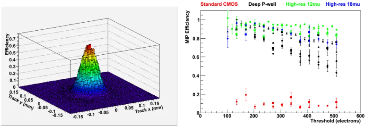
The UK groups in SPiDER have demonstrated that the INMAPS technology developed specifically for the DECAL application is viable in terms of basic pixel efficiency. INMAPS is implemented as a 0.18µm CMOS process in which a deep P-well implant stops signal charge from being absorbed in N-well circuits, and therefore allows the use of both NMOS and PMOS within the pixel, as well as (optionally) high resistivity silicon in the thin epitaxial layer to reduce the charge collection time.