All Inorganic Colloidal Quantum Dot LEDs
by
Vanessa Claire Wood
Submitted to the Department of Electrical Engineering and Computer
Science
in partial fulfillment of the requirements for the degree of
Masters of Science in Computer Science and Engineering
at the
MASSACHUSETTS INSTITUTE OF TECHNOLOGY
June 2007
©
Massachusetts Institute of Technology 2007. All rights reserved.
A u th o r ... .. . ... ...
Department of Electrical Engineering and Computer Science
May 2007
14Certified by...
Accepted by
MASSACHUSETTS INSTnTUTE OF TECHNOLOGYAUG 16 2007
. 1
...
Vladimir Bulovid
Associate Professor
Thesis Supervisor
.... c . . - - - ... ....Arthur C. Smith
Chairman, Department Committee on Graduate Students
All Inorganic Colloidal Quantum Dot LEDs
by
Vanessa Claire Wood
Submitted to the Department of Electrical Engineering and Computer Science on May 11, 2007, in partial fulfillment of the
requirements for the degree of
Masters of Science in Computer Science and Engineering
Abstract
This thesis presents the first colloidal quantum dot light emitting devices (QD-LEDs) with metal oxide charge transport layers. Colloidally synthesized quantum dots (QDs) have shown promise as the active material in optoelectronic devices because of their tunable, narrow band emission. To date, the most efficient QD-LEDs involve a mono-layer of closely packed QDs sandwiched between organic charge transport mono-layers. However, these organic materials are subject to degradation due to atmospheric oxy-gen and water vapor. In contrast, metal-oxide films used in this work are chemically and morphologically stable in air and can withstand numerous organic solvents, which increases the flexibility of device processing. Furthermore, they can sustain higher carrier injection rates needed to realize an electrically pumped colloidal QD laser. This thesis details the characterization techniques, such as Atomic Force Microscopy, photoluminescence spectroscopy, Hall Effect measurements, X-Ray Diffraction, and Ultraviolet Photoelectron Spectroscopy, used to design efficient QD-LEDs. It reviews the steps used to optimize device performance and obtain a transparent device ar-chitecture with external quantum efficiency of 0.15% and a peak luminance of 7000 Cd/m2. This manifests a 100-fold improvement in efficiency over any previously re-ported all inorganic QD-LED structure.
Thesis Supervisor: Vladimir Bulovid Title: Associate Professor
Acknowledgments
Many thanks to my advisor, Professor Vladimir Bulovid for his guidance, enthusiasm, and encouragement.
Many coworkers deserve recognition. Special thanks goes to Jean Michel Caruge for teaching me about RF sputtering and for our brainstroming sessions, to Jonathan Halpert for synthesizing the quantum dots used in this work, and to Dr. Peter Mardilovich for his insights on metal oxides. I would also to thank Alexi Arango, Polina Anikeeva, Gerry Chen, Kaveh Milaninia, James Perkins, and Venda Porter for their assistance with various aspects of this work. And thanks to all in the Bulovi group for making lab such a fun place to be.
This research was supported by NSF-MRSEC, NSF-NIRT, a Presidential Early Career Award for Science and Engineering, the Institute for Soldier Nanotechnologies, and a National Defense Science and Engineering Graduate Fellowship.
Contents
1 Introduction 15
1.1 Quantum Dot LEDs . . . . 15
1.1.1 Limits of Organic QD-LED Technology . . . . 19
1.1.2 QD-LED function ... 20
1.2 All-inorganic QD-LEDs ... 21
1.3 Q D-Lasers . . . . 26
2 Material Properties and Growth 27 2.1 M etal Oxides . . . . 27
2.2 Radio Frequency Magnetron Sputtering . . . . 32
2.3 Quantum Dots . . . . 35
2.4 Colloidal Quantum Dot Synthesis . . . . 38
3 Design of All-Inorganic QD-LEDs 43 3.1 Characterization of Sputtered Films . . . . 43
3.1.1 Atomic Force Microscopy . . . . 43
3.1.2 X-Ray Diffraction . . . . 45
3.1.3 Hall Effect Measurements . . . . 49
3.2 The Quantum Dot-Metal Oxide Interface . . . . 51
3.2.1 Atomic Force Microscopy . . . . 51
3.2.2 Quantum Dot Luminescence Quenching . . . . 53
3.2.3 Summary of Sputtering Parameters of Ceramic Materials . . . 54
3.3.1 M etal Oxides . . . . 59
3.3.2 Quantum Dots . . . . 63
4 All Inorganic QD-LEDs 67 4.1 Measurement Techniques ... 67
4.2 All Inorganic QD-LEDs . . . . 68
4.3 Improving Efficiency with ZnS . . . . 72
4.4 Improving Efficiency with ZnO . . . . 73
4.5 Transparent QD-LEDs . . . . 77
4.6 Toward Green and Blue All Inorganic QD-LEDs . . . . 80
List of Figures
1-1 Schematic of liquid crystal cell [1]. . . . . 16
1-2 Room temperature optical absorption spectra of CdSe QDs dispersed in hexane
[2].
Varying the size of the QD, tunes its optical properties continuously through the visible spectrum. This is not possible for any type of organic lumophore. The photograph of the QDs excited by UV light reveals their high photoluminescence efficiencies through the visible region of the spectrum. . . . . 181-3 a) Normalized electroluminescence spectra for QDs showing their nar-row band emission throughout in the visible and infrared region of the spectra [3], [4]. b) White QD-LED made by sandwiching a monolayer of mixed red, green, and blue QDs between organic charge transport lay-ers [5]. c) RGB pixels, 25 by 25 pm, featuring electroluminescence from red and green QDs and blue emission from the organic hole transport layer, N,N'-Bis(3-methylphenyl)-N,N'-bis(phenyl)benzidine (TPD) [6]. 19
1-4 A schematic of the (a) structure and (b) band diagram of a typical QD-LED structure. The schematic in (c) depicts the injection of charge into device and the formation of excitons across the QD layer for a QD-LED under forward bias. . . . . 21
1-5 a) An SEM image showing the device structure composed of a col-loidal CdSe/ZnS QD layer sandwiched between a p-type, MOCVD, GaN layer grown on a sapphire substrate and a n-type GaN layer grown using ENABLE. b) Photographs of the device electroluminescence at 10 and 30 V for which non-uniform emission is evident. The white arrow points to blue emission from the GaN. [7] . . . . 23 1-6 a) EL spectrum for hybrid organic-inorganic device made with QDs
sandwiched between a sputtered NiO HTL and an organic (Alq3) ETL biased at 9 V. b) i-v and EQE curves for device. . . . . 25 2-1 Disordered Kronig Penny model (a) potential and (b) resulting
wave-function. . . . . 28 2-2 Schematic of the density of states for an amorphous solid
semiconduc-tor at different energies. . . . . 29 2-3 Localized electron hopping model. . . . . 31 2-4 Cross sectional view of electrode assembly for RF sputtering. . . . . . 34 2-5 Schematic depicting synthesis procedure for CdSe as first described in [2]. 39 2-6 Schematic of the structure of a) ZnCdSe, b) (CdSe)ZnS, c) ZnSe/CdSe/ZnS,
and d) ZnCdS QDs . . . . 40 3-1 Atomic Force Microscopy surface topography images of a) ITO
RF-sputtered on glass, and b) NiO RF-RF-sputtered onto the ITO shown in (a) . . . . 44 3-2 Atomic Force Microscopy surface topography images showing smooth
ZnO : SnO2 on top of the ITO in Figure 3-la . . . . 45
3-3 X-ray diffraction spectra for a) RF-sputtered ITO, b) RF-sputtered
ITO in a heated chamber, and c) commercially purchased ITO. . . 47
3-4 X-ray diffraction spectra for NiO, ZnS, ZnO, and ZnO : SnO2. . . . .. 48
3-5 AFM images of a) QDs stamped onto NiO, b) QDs in chloroform spun onto NiO, and c) QDs in a 9:1 hexane to octane solution spun onto NiO. 52
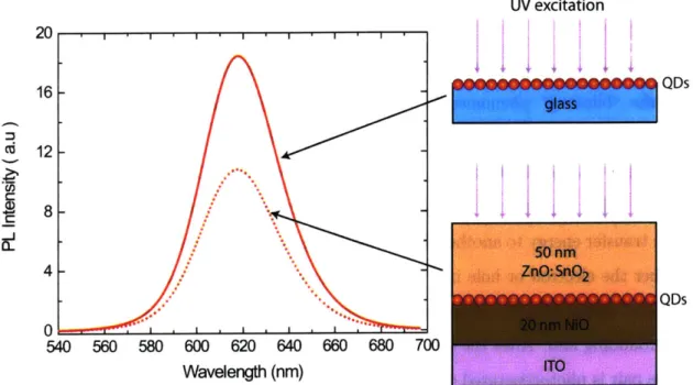
3-6 PL spectrum of 30 nm thick CdZnSe QD layer on glass (solid red line) and 30 nm thick CdZnSe QD layer between NiO and ZnO:SnO2
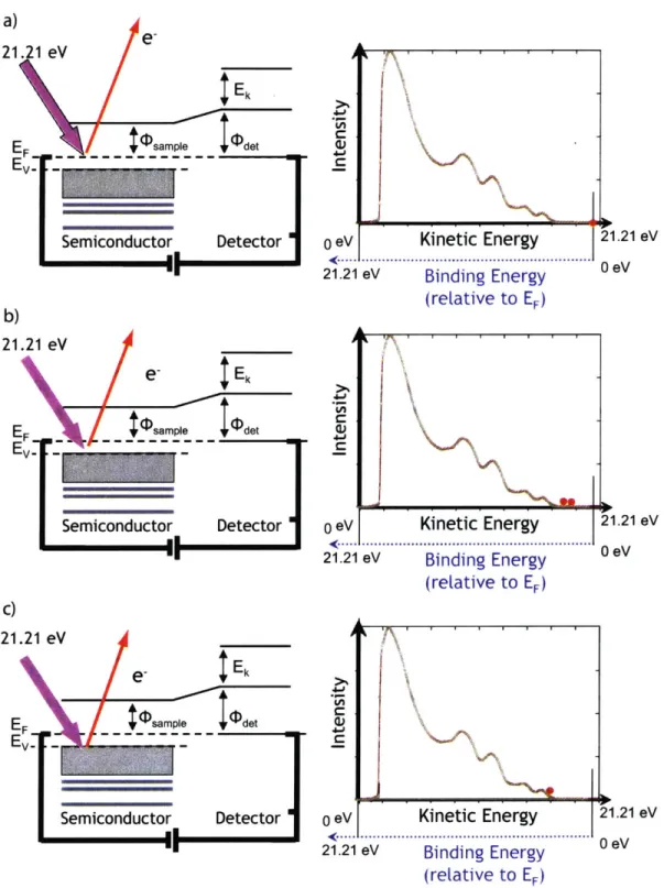
(dotted red line). The two samples, shown schematically to the left, were excited within the same optical geometry using a UV lamp. We measured a 40% drop in the PL intensity on average. . . . . 54 3-7 Schematics explaining key features of the UPS spectrum of a
semicon-ductor... 57 3-8 Schematics explaining key features of the UPS spectrum of a
semicon-ductor... 58 3-9 UPS spectra for ITO. . . . . 60
3-10 UPS spectra for ZnO, SnO2, and ZnO : Sn02 . . . . . . . 61 3-11 a) The UPS spectrum for ZnS on an ITO substrate at 6V reserve bias.
b) A close up of spectrum for low kinetic energy electrons reveals an onset at 4.87 eV. c) The derivative of the intensity spectrum for large kinetic energy electrons reveals a 2.55 eV gap between the Fermi level and the valence band . . . . 62 3-12 Absorption spectra of QDs following different treatments for removing
the ligands. . . . . 64 3-13 UPS spectra for CdSe QDs. The spectrum in (a) gives the number
of electrons hitting the detector each second as a function of electron energy. The spectrum was taken with the sample reversed biased at 6V to create a sharper turn on. The plot in (b) is the derivative of the signal at higher electron energies. No bias was applied for this m easurem ent. . . . . 65 3-14 AFM of a CdSe QD film on ITO after soaking it in a solution of 0.1M
butylyamine in acetonitrile for 5 minutes and baking at 70 C for 30 m inutes. . . . . 66 4-1 Device schematic and approximate band structure as determined by
4-2 The J-V curve for the first all-inorganic QD-LED and band diagram schematic under forward bias . . . . 70 4-3 EL spectrum showing emission entirely from QD layer. Photograph of
emission from the device at 6 V applied bias. . . . . 71 4-4 EQE as a function of current density for the first metal oxide based
QD-LED. Maximum EQE for this device is 0.09%. The inset shows that a maximum luminance of 7000 Cd/M2 is reached at 3.5 A/M2 . . 72
4-5 Schematic of device structure and proposed band diagram, under for-ward bias, containing ZnS electron blocking layer. . . . . 73 4-6 J-V and QE of all inorganic QD-LED with a ZnS electron blocking layer. 74
4-7 EL of all inorganic QD-LED with a ZnS electron blocking layer. . . . 74
4-8 Schematic of device structure with an insulating ZnO layer, and EL spectrum of device biased at 10 V and showing emission entirely from QDs. ... 75 4-9 J-V and EQE plots for device with an insulating ZnO layer. . . . . . 75 4-10 Schematic of device and EL spectrum at 10 V showing emission entirely
from Q D s. . . . . 76 4-11 J-V and EQE for ITO/ZnO : SnO2/ZnO/QD/ZnO/ZnS/ZnO : SnO2/Ag
structure. ... ... 77 4-12 A schematic of the structure of the first transparent QD-LED. A SEM
cross sectional image is shown to the right. . . . . 78 4-13 Photographs of a transparent all inorganic colloidal QD-LED. ... 79 4-14 J-V and EQE characteristics for a transparent QD-LED. . . . . 79 4-15 Band diagram showing reserve and forward bias applied to the
trans-parent QD-LED structure. . . . . 81 4-16 CIE chromaticity diagram showing the current NTSC standard and
location of QDs on the CIE diagram. . . . . 82 4-17 J-V plots comparing green and red QD devices. . . . . 83
4-18 Band diagram in forward bias for proposed device structure. EL spec-tra for green and blue QD devices. The broad band emission is indica-tive of W 03 emission . . . . 84
Chapter 1
Introduction
In this thesis, I report the development of thin film light emitting devices (LEDs) with metal oxide charge transport layers and colloidal quantum dots (QDs) as the ac-tive emissive layer. Chapter 1 reviews the operation of organic light emitting devices (OLEDs) and the benefits of integrating of colloidal QD into the OLED structure. It also motivates the development of all-inorganic LEDs with QDs as the luminescent medium. Chapter 2 explores the basic physical properties and growth techniques associated with QDs and metal oxides that make them an attractive material set with which to fabricate the all-inorganic QD-LEDs. Chapter 3 discusses characteri-zation techniques, such as Atomic Force Microscopy, Hall Effect measurements, X-ray diffraction, and Ultraviolet Photoelectron Spectroscopy, used to design efficient QD-LEDs. Chapter 4 presents the first examples of all-inorganic QD-QD-LEDs.
1.1
Quantum Dot LEDs
There are several technologies that must be discussed in order to illustrate the poten-tial benefits of using QD-LEDs for displays. Liquid crystal displays (LCDs) currently dominate the flat panel display market. LCDs are essentially voltage driven light switches that allow white light from a back plane to either be transmitted or ab-sorbed. The schematic in Figure 1-1 can aid in understanding their operation. Light from the backplane passes through a polarizer and then through the liquid crystals,
INCIDENT INCIDEDU
UNPOL.ARISED POLARISER UNPOLARISED
LIGHT LIGHT SUBSTRATE ELECTRODE +ALIGNMENT ElECTRODE +ALIGNMENTf SUBSTRATE POLARISED LIGHT LIGHT ABSORBED TRANSMITED
IN THE OFF-STATE POLARISER IN THE ON-STATE
Figure 1-1: Schematic of liquid crystal cell [1].
which can be aligned with application of an electric field. Liquid crystals are birefrin-gent, which means that depending on their orientation relative to the incoming light, the polarization of the light can be rotated. This light then impinges on a second polarizer oriented perpendicular to the first polarizer. The amount the polarization of the light is rotated while traversing the liquid crystals determines the amount of light transmitted through the liquid crystal cell. Any transmitted light then passes through a color filter to provide red, green, and blue (R.GB) pixels. However, LCDs have sev-eral important limitations including narrow viewing angle, limited color range, low power efficiency because of the use of filters, and slow switching speeds between the on and off state of each pixel.
Inorganic LEDs (ILEDs) are used primarily for indicator lights and back plane sources for LCD displays. Because ILEDs involve epitaxial growth of single crystals of semiconductor on lattice-matched substrates, their cost has made them prohibitively expensive for most large area lighting applications.
organic molecules for light emitting devices [8]. In contrast to ILEDs, organic LEDs (OLEDs) offer extremely cheap production. Furthermore, unlike LCDs, OLED dis-plays maintain color verity at any viewing angle. OLED disdis-plays are now commer-cially available in cell phones, digital cameras, and PDAs, and flat panel screens. However, OLEDs have been slow to enter the market because of some fundamental physical limitations for which solutions are not immediately obvious. For one, the human eye is most sensitive to green light, and finding red and blue emitters efficient enough to match the perceived brightness of green lumophores has been a challenge. Compounding this problem is the fact that organic materials are broad band emitters, so blue emitters typically appear blue-green or emit excessive amounts of UV light. Secondly, an efficient process for laterally patterning red, green, and blue emitters has yet to be developed. Standard lithographic procedures, such as photoresist spinning, baking, and stripping, are not compatible with organic materials.
Using colloidal quantum dots (QDs) as luminescent dopants in OLEDs offers an attractive solution to the challenges described above. QDs are nanoparticles that can be synthesized to emit anywhere from the ultraviolet to the infrared regions of the spectrum by changing their size and chemical composition [2]. For example, as shown in Figure 1-2, varying the size of CdSe QDs between 17 to 120
A tunes them
to absorb and emit at colors ranging from blue to red. The typical emission spectrum of a QD has a full width half maximum of less than 40 nn, meaning it has excellent color saturation. Colloidal QDs routinely have high photoluminescence efficiencies of 40-60%) that can reach 90 % in synthetic procedures. Furthermore, QDs do not photobleach as do organic lumophores.QDs were first integrated into a polymer LEDs in 1994 [9]. Inserting a single close-packed monolayer of QDs into an OLED structure yielded a device with a peak external quantum efficiency (EQE) of 0.52% [10]. Narrowband electroluminescnece, shown in Figure 1-3a, has been observed in QDs throughout the visible and the infrared [3], [4]. QD-LEDs with organic charge transport layers now boast EQEs of about 2% in the red, 0.5% in the green, and 0.2% in the blue [5]. Figure 1-3b displays a picutre of a white LED with an EQE of 0.36% under 10 V applied bias, which was
C 0 0. D Di eter= 120A 80A 72A 55A 45A 33A 29A 20A 1 7A 400 500 600 700 Wavelength (nm)
Figure 1-2: Room temperature optical absorption spectra of CdSe QDs dispersed in hexane [2]. Varying the size of the QD, tunes its optical properties continuously through the visible spectrum. This is not possible for any type of organic lumophore. The photograph of the QDs excited by UV light reveals their high photoluminescence efficiencies through the visible region of the spectrum.
I I * I I * I a. E 2 -j w
7I
N
400 500600 1200 Wavelength (nm) 1400 i6oFigure 1-3: a) Normalized electroluminescence spectra for QDs showing their narrow band emission throughout in the visible and infrared region of the spectra [3], [4]. b) White QD-LED made by sandwiching a monolayer of mixed red, green, and blue QDs between organic charge transport layers [5]. c) RGB pixels, 25 by 25 pm, featuring electroluminescence from red and green QDs and blue emission from the organic hole transport layer, N,N'-Bis(3-methylphenyl)-N,N'-bis(phenyl)benzidine (TPD) [6]. created by sandwiching a monolayer of mixed red, green, and blue QDs between organic hole and electron transporting layers [5]. Deposition of this QD monolayer was enabled by a microcontact printing technique [6]. By patterning the stamp used in this printing process, RGB pixels 25 by 25 gm were achieved. Figure 1-3c shows such a display, created by stamping perpendicular lines red and green QDs. The blue emission comes from the organic hole transport layer, N,N'-Bis(3-methylphenyl)-N,N'-bis(phenyl)benzidine (TPD). These results demonstrate that QD-LEDs are a promising technology for displays and large area lighting.
1.1.1
Limits of Organic QD-LED Technology
Hybrid organic-inorganic QD-LEDs combine the benefits of two material sets: organ-ics offer ease of fabrication while the inorganic nanocrystals provide efficient, tunable,
40
narrow-band emission. However, hybrid QD-LEDs also retain one of the major prob-lems facing organic LEDs (OLEDs). Namely, the organic charge transport layers of hybrid QD-LEDs are susceptible to photooxidation from self-emitting light, ther-mal and electrochemical degradation, and deterioration from atmospheric oxygen and water vapor [11, 12, 13, 14]. A variety of packaging techniques, including the simple solution of a cover glass epoxied to the sample [15], have successfully increased the operating lifetime and allowed OLEDs and hybrid QD-LEDs to become commercially viable. However, packaging comprises a significant fraction of the device cost making it difficult for QD-LEDs to compete with the already established technology of LCDs. Furthermore, organic materials undergo a change in morphology and decompose at high drive currents, which frustrates development of an electrically pumped colloidal QD laser.
My thesis explains how the organic charge transport layers in the QD-LED struc-ture can be replaced with chemically and morphologically stable metal oxides to achieve robust and efficient devices that can operate unpackaged in air and sustain high current densities.
1.1.2 QD-LED function
Before discussing the prior work on QD-LEDs with inorganic charge transport layers, it is important to review basic structure and functioning of a QD-LED. As depicted in Figure 1-4, the simplest QD-LED consists of a hole transport layer (HTL), a QD layer, and an electron transport layer (ETL) sandwiched between two electrodes. Typically the HTL and ETL are each approximately 50 nm thick, and the QD region ranges from a monolayer to several monolayers of QDs. A band diagram for such a device is shown schematically in Figure 1-4b. When the device is in forward bias (See Figure 1-4c), the anode injects holes into the HTL while the cathode injects electrons into ETL. The field across the device carries the holes and electrons to the QD layer, where the electrons and holes can form bound pairs, known as excitons, on the QDs. Excitons can dissipate their energy by emitting light characteristic of the optical bandgap of the QDs.
b.
a..
J__ ETL
Q~~spotons s
Figure 1-4: A schematic of the (a) structure and (b) band diagram of a typical QD-LED structure. The schematic in (c) depicts the injection of charge into device and the formation of excitons across the QD layer for a QD-LED under forward bias.
1.2
All-inorganic QD-LEDs
There are two types of QDs: epitaxial and colloidal. Colloidal QDs are synthesized from organometallic precursors injected into an organic solvent at high temperature. The temperature activates nucleation of small crystallites, which continue to grow from the unreacted precursors until stopped by cooling. This procedure allows for fine control over QD size and results in a very monodisperse solution. The synthesis also leaves colloidal QDs coated in organic ligands so that the QDs can be made soluble in a diverse set of solvents including chloroform, hexane, ethanol, and even water. Colloidal QDs are therefore solution processable and can be patterned on substrates using large scale techniques such as spin coating, microcontact-printing, and inkjet deposition. Epitaxial QDs, often known as self-assembled QDs (SAQDs), form when a semiconducting material is deposited, generally through molecular beam epitaxy (MBE), on a substrate having a different lattice constant or at a very high rate. Strain causes the top material buckle and form QDs, in what is referred to as Stranski-Krastanow growth. MBE can then be used to deposit a capping layer and the top charge injection layer [16]. As grown, SAQDs are already integrated into a
monolithic semiconductor structure making them a seemingly obvious choice for a robust and stable all-inorganic LED structure.
However, colloidal QDs possess properties that make them superior to epitaxial QDs for optoelectronic applications. Epitaxial QDs do not offer the monodispersity, the high photoluminescence intensities, the low cost, or the easy fabrication advan-tages of colloidally grown QDs. Also, the size of an epitaxial QD is determined by the material set available. This prevents integration of more than one color QD into the simple three-layer structure described in Section 1.1.2, making it difficult to realize RGB pixels or white light LEDs. For these reasons, my thesis focuses on the devel-opment of LEDs with colloidal QDs sandwiched between inorganic charge transport layers.
So far, several methods for integrating colloidal QDs into inorganic heterostruc-ture have been proposed, but have only met with limited success. Early attempts to use inorganic transport materials in QD-LEDs placed QDs between indium tin oxide (ITO) and silver electrodes [171. The low efficiency of about 10-3 cd/A in these devices is probably due to quenching of the QD luminescence by the highly conduc-tive electrodes [18]. A novel fabrication technique, which was used to build the first all inorganic colloidal QD device exhibiting narrow-band electroluminescence (EL), is known as energetic neutral atom beam lithography/epitaxy (ENABLE) [7]. Thin films grown using ENABLE are similar to those grown with metal-organic chemical vapor deposition (MOCVD), but ENABLE does not require elevated substrate tem-peratures and organometallic precursors, which destroy the luminescent properties of QDs. ENABLE involves a chemical reaction on the sample surface between a beam of neutral atoms, such as nitrogen, and a metal, like gallium, that is simultaneously deposited via e-beam evaporation. Low temperature ENABLE (300 C) allows depo-sition of GaN on the QDs without compromising their performance; in fact, the GaN acts as an encapsulating layer, reducing the photo-oxidation of the QDs. As depicted in Figure 1-5a, the devices themselves consist of a Langmuir-Blodgett film of colloidal CdSe/ZnS QDs sandwiched between a p-type, MOCVD, GaN layer grown on a sap-phire substrate and a n-type GaN layer grown using ENABLE. The device is reported
a.
SEM image
Figure 1-5: a) An SEM image showing the device structure composed of a colloidal CdSe/ZnS QD layer sandwiched between a p-type, MOCVD, GaN layer grown on a sapphire substrate and a n-type GaN layer grown using ENABLE. b) Photographs of the device electroluminescence at 10 and 30 V for which non-uniform emission is evident. The white arrow points to blue emission from the GaN. [7]
to exhibit no degradation after several months; however, as shown in Figure 1-5b, its operating voltages are fairly large and there is non-uniform illumination of each pixel. At 30 V, blue GaN emission is observed. Furthermore, the EQE was small (0.001 to 0.01%).
Integration of colloidally and epitaxially grown QDs has been proposed as another strategy for obtaining an all inorganic device although demonstration of EL has yet to be realized in such a structure. One study describes a hybrid structure where colloidally grown InAs QDs are deposited on top of a GaAs SAQD structure grown using MBE [19]. Migration enhanced epitaxy (MEE), which is a low temperature (350 C) technique similar to MBE, is then used to overcoat the colloidally grown InAs QDs with epitaxial GaAs. This design combines the structural benefits of SAQDs with the highly photoluminescent (PL) efficiencies of colloidal QDs. Another study
investigated the reverse process of growing epitaxial QDs on colloidal QDs to eliminate nonuniformities in QD size at their interface with the charge transport layers [20]. Specifically, CdSe(ZnS) core shell QDs are overcoated with ZnSe deposited via MEE. Previous research in our group has shown that replacing the organic charge trans-port layers with metal oxides is a viable approach to creating a more chemically and electrically stable QD-LED. Uniform EL was achieved by replacing an organic hole transport material with p-type nickel oxide (NiO) and continuing to use the standard organic material, Tris-(8-hydroxquinoline) aluminum (Alq3) as the electron transport layer [21]. To fabricate this device, NiO was radio-frequency magnetron sputtered in an argon and oxygen environment onto conductive indium tin oxide (ITO), which serves as the anode. The oxygen content of the plasma during sputtering as well as the deposition rate determined the number of excess hole donor sites (the extent of the p-type doping) of the NiO. To complete the device, which is depicted in the inset of Figure 1-6a, QDs were spin coated on top of the NiO, and Alq3 and a silver electrode were thermally evaporated on the QDs. The spectrum in Figure 1-6a shows EL characteristic of the QDs, and a peak external quantum efficiency (EQE) of 0.18% was observed (See Figure 1-6b).
This work demonstrated three areas where, if metal oxides are to be used as the charge transport layers of a QD-LED. considerable improvement is needed. First, the device yield of 10% and the low EQE suggest that much of the injected current is shunted through the device structure due to ITO and NiO surface roughness. Second, QD luminescence is most likely quenched by free carriers in the NiO layer. Third, differences in carrier mobilities in the Alq3 and NiO layers can cause either electron or
hole pile up at the QD layer. This can result in charging of the QDs and subsequent Auger processes, which can contribute to diminished device EL.
The goal of my thesis work was to address these three areas limiting the integration of metal oxides into the QD-LED structure and to investigate whether metal oxides can be successfully deposited onto top of QDs to form a high efficiency, all-inorganic
a. 12 -200 b. 0.1 0 wj 0.01 1 E-3 300 400 500 600 700 Wavelength (nm) 14-12 r 0101 8 8 S61 S4. - 2 -4 6 8 10 12 14 16 18-. , i i , i V ltag (V 800 6 8 10 12 14 16 18 Voltage (V)
Figure 1-6: a) EL spectrum for hybrid organic-inorganic device made with QDs sand-wiched between a sputtered NiO HTL and an organic (Alq3) ETL biased at 9 V. b) i-v and EQE curves for device.
. I * I I * QDs -p -l C 4 8
1.3
QD-Lasers
An ideal QD is a 0-dimensional structure; an electron in it is confined in all-directions as if in a box. The QD density of states given by a series of 6 - functions at the en-ergies corresponding to the discreet levels allowed in the "box". These quantized levels give the QD atom-like electronic and optical properties. Because of these char-acteristics, a semiconductor laser with a QD active region promises, among other advantages, low and temperature-independent threshold current and high-frequency modulation with negligible chirping effects (small linewidth enhancement). [22]
In 1993, a laser based on epitaxially QDs was realized [23]; however, a QD laser operating at room temperature has yet to exhibit a better modulation bandwidth and a smaller linewidth enhancement factor than a quantum well lasers [24]. A large mod-ulation bandwidth is possible if the structure has large differential gain [25]. A large differential gain is predicted for a structure with a high density of QDs [24]. However, multilayered epitaxial QD growth is challenging and leads to nonuniformities in QD size. This causes an inhomogeneous broadening of about 10 to 30 meV [26], which in turn results in a reduced differential gain [24].
In contrast to epitaxial QDs, colloidal QDs have better size distribution and can be easily deposited in densely packed multilayers. To date, however, the only efficient electroluminescent colloidal QDs structures involve a monolayer of close-packed QDs sandwiched between organic layers for charge transport and injection. As discussed in Section 1.1.1, the Van der Waals-bonds of organic materials can not support the high current densities required for laser operation. Metal oxides have primarily covalent
and ionic bonds, suggesting that they can sustain much higher current fluxes than organics. Data presented in Chapter 4 indicates that colloidal QD and metal oxide structures may be the key to a high-frequency modulation and small chirp laser.
Chapter 2
Material Properties and Growth
2.1
Metal Oxides
Metal oxides, and ceramic materials in general, are attractive charge transport lay-ers because of their great range of electrical properties. Ceramics typically have the chemical formulas: MaXc or MaNbXc, where M and N are metals, and X is a non-metallic element [27]. They can be non-metallic (e.g. TiO2), insulating (e.g. ZnO or NiO), or semiconducting (e.g. nonstoichiometric ZnO or NiO). In this thesis, I will discuss the electronic ceramics indium oxide (In203), nickel oxide (NiO), tin oxide
(SnO2), zinc oxide (ZnO), tungsten oxide (W0 3), and zinc sulfide (ZnS).
There are two types of bonding in these materials: ionic and covalent bonds. Ionic bonds are defined by the Coulombic attraction between oppositely charged ions and result in insulating materials with very strong, non-directional bonds. Ionic bonding occurs if the energy of the molecular unit is lower than the energy of the separated ions. Covalent bonding, on the other hand, is the sharing of electrons. The electrons reside somewhere between the two atoms, in a configuration that depends on which electronic orbitals are sharing the electrons. This can lead to directional bonds. In ceramic materials, the valence electrons of the metal ions are shared with the valence shell of the nonmetal ion, which leads to bonds that range from highly covalent to highly ionic. [28]
a.
x b.
x
Figure 2-1: Disordered Kronig Penny model (a) potential and (b) resulting wavefunc-tion.
its microstructure can range from crystalline to amorphous. In this work, we aim for amorphous ceramic charge transport layers so that charge travels through the bulk of the materials instead of along grain boundaries or defects in a crystalline or poly-crystalline layers. This assures more uniform charge transport that will be immune to defects in the charge transport layers. While the band theory and consequently, electronic transport, of crystalline ceramics is well understood, amorphous materials lack periodic boundary conditions and long range order. In an amorphous material, the wavefunction loses phase coherence over several atomic spacings. Some under-standing can be gained from modeling an amorphous material with one-dimensional Kronig-Penny model where the finite square well potentials are spaced at random intervals as depicted in Figure 2-1a. This potential has a wave packet solution, shown in Figure 2-1b, and given by:
c e^Ixasin(kx) (2.1)
This model implies that all electronic states in an amorphous solid are localized [29]. Extending the finite square well problem to two or three dimensions however indicates that there can be both localized and extended electronic states. Figure 2-2 shows a typical electronic density of states. The extended states (or Bloch states) resemble conduction and valence bands in a crystalline material. Disorder in the solid leads to exponential band tails [30]. Defects in the crystal result in mid-gap states.
Extended States EB ... Diffusion Ec .States Mobility Gap C E> (Localized States) Ev ... Density of States
Figure 2-2: Schematic of the density of states for an amorphous solid semiconductor at different energies.
The band tail and mid-gap states are localized states and lie in a region of the band diagram known as the mobility gap.
A quantity known as the Anderson parameter quantifies the degree of electron
localization of a particular state. The Anderson parameter, A, is given by:
A = (2.2)
AE d.''
J is the overlap integral of periodic basis states, coupled by nearest neighbor
inter-actions. Disorder is introduced into the model by assuming that each basis states resides at a different site energy spanning a width, AE:
J = E ZJ 0,Vn,kidr3 (2.3)
n~i
where i electron wavefunction of the ith state, Vn is the interaction potential of the nth site. When the Anderson parameter is small (about 0.2), all states can be considered localized. In metal oxides, there is typically some critical energy, Ec, below which all states are localized. This energy is typically slightly less than EB, the mobility edge. [29]
ex-hibit different mechanisms for charge transport. Above the mobility edge (EB), there is band conduction as in crystalline semiconductor, although with considerably lower mobility because of scattering events from the disorder in the lattice. Between EB
and Ec, electrons move via diffusion, and below E, via thermally activated hopping. In the diffusion transport regime between EB and Ec, the electronic wavefunctions are highly modulated, meaning that there are alternating regions of high and low probabilities of finding an electron. Ignoring the possible interaction of the electron and the lattice and the subsequent formation of polaron states, the mobility of an electron is:
ea =
(2.4)
Tg =FVel
where a is the distance between the electronic wavefunction maximum and minimum and vij is the frequency that an electron is at a maximum. [27]
The classical picture of the "hopping" transport mechanism is shown schematically in Figure 2-3. Assume two localized sites, separated by energy AE (Figure 2-3a). An electron localized on site 1, can, with thermal energy, polarize the lattice(Figure 2-3b). The binding energy of the electron (Eb), which is the sum of energy required to polarize the lattice and energy the energy the electron gains from polarizing the lattice, is given by:
e2 1 1
Eb = -( ) (2.5)
2ro k. k,
where ro is the radius of the electronic state, and k, and k, are the infinite-frequency and static dielectric constants, respectively. For the electron to hop to site 2, the electronic energies of the states must be equal(Figure 2-3c). The difference in energy between this equal energy configuration and the original energy configuration with the sites separated by AE is called the hopping activation energy and is given by:
AE Eb (AE)2 (2.6)
2 2 8Eb
a) Site 1 Site 2 Ef ... ... ... -...- AE b) Ef -..--.-- ...-- .. 2Eb f) E..-.-- -... . Eb6+AE Eb -A 2 2 ... 2Eb
Figure 2-3: Localized electron hopping model.
2 with a probability, p = exp(-2ad). This gives a transition rate of:
-EH
W=pvexp
'
(2.7)where v is the phonon frequency. If two sites are close enough together, adiabatic hopping can take place, in which an electron tunnels repeatedly between site 1 and 2, aided by a resonance process. [27].
This "hopping" conduction is the primary mode of charge transport in the mid-gap defect states. In metal oxides, defects can arise from dopants, vacancies, or structural variations, and are extremely important in defining the electrical properties of the material. In this work, the most important electronic defects result from the reduction or oxidation of the metal ions, which can be controlled with the oxygen partial pressure during the oxide growth [31]. At low oxygen concentrations, material can lose oxygen and generate electrons that contribute to n-type conductivity:
00 -- -02 +V + 2e// (2.8)
The nomenclature indicates that when a vacancy V'* is created at a previously occu-pied oxygen site (O.), free oxygen molecules (On) and electrons 2e// result. If there is instead a surplus of oxygen, it can fill an oxygen vacancy, leaving two holes and contributing to p-type conduction:
1
-02 + V * -- O00 + 2h' (2.9)
2
We note that while ZnO and NiO are both insulating metal oxides, oxygen depletion leads to n-type ZnO (Zni+,O.) and oxygen doping results in p-type NiO (Ni,0 1+,).
As will be discussed in Chapters 3 and 4, this fine tuning of the conductivity offered by metal oxide proves crucial to the development of efficient all-inorganic QD-LEDs.
2.2
Radio Frequency Magnetron Sputtering
We choose radio-frequency (RF) magnetron sputtering to deposit the ceramic thin films. RF magnetron sputtering rates are similar to those of thermal evaporation, making it a fast deposition technique compared, for example, to MBE, MEE, or ENABLE that have been used in previous attempts to make all-inorganic QD-LEDs. In the sputtering process, energetic ions bombard a target, causing atoms to be ejected from the target and land on a substrate, which, in our system, is located above the target. The ions are provided by a plasma, which is generated by flowing gas, typically Argon, between two electrodes. An electron. accelerated by the potential between the electrodes, collides with an Argon atom resulting in an Argon ion (Ar+), a free electron (ei 0,), and the now much slower original electron (e owed). Symbolically, this
reaction, can be summarized by:
efast + Ar -+ Ar++e- + e-wed (2.10)
e~owe- and e-0 are accelerated by the field between the electrodes. When these
electrons attain 15.76 eV of energy, which is the ionization energy of Ar, they can each cause the reaction of Eqn. (2.10). The creation of Ar ions is therefore an avalanche
process. [32]
To understand RF sputtering, it is useful to review the mechanism for gas dis-charge in DC sputtering. In DC sputtering, a voltage is applied between an anode and a cathode, and ions are attracted to the cathode while electrons are repelled. This surplus of ions screens the negative charge of the cathode, causing most of the voltage to be dropped across an area close to the cathode, which is known as Crook's Dark space. In this space, electrons are accelerated away from the cathode to ionize Ar atoms as described previously. Meanwhile, this voltage drop accelerates ions toward the cathode. The cathode is also the sputtering target, so ions etch microscopic bits of material from target. In this work, we consider relatively low energy sputtering so the process can be modeled as momentum transfer through elastic collisions. The maximum energy transferred in a collision between the ion (with mass M1 and energy
E) and a target atom (with mass M2) is:
4M A12 E (2.11)
(Al1 + M2)2
This corresponds to a sputtering yield:
S 0C 1 A 1 2 E (2.12)
A(E)cosO (M1 + A2)2
where 9 is angle between the target surface normal and the incident ions and A(E) is the mean free path for ions near the target surface [33]. These calculations in-dicate that sputtered atoms leave the target with kinetic energies of 3-10 eV. Our rf-sputtering is done at pressures of 4-6 mTorr, and the sputtered atoms undergo collisions with gas atoms in the chamber. When they arrive at the substrate, which is located between 5 and 6 inches from the target, the atoms have approximately 1-2 eV of energy.
The process described above is DC sputtering; in RF sputtering, the anode and cathode are reversed at radio-frequencies. In our chamber, the polarity is alternated at a standard 13.65 MHz. RF sputtering gives a greater range of material choices than
Ar ions RF electrode ta rget grounded neshield watercooling Argon to RF power gas supply
Figure 2-4: Cross sectional view of electrode assembly for RF sputtering.
were placed at the cathode, positive charge would accumulate on the target during the ion bombardment. This would neutralize the cathode voltage, gradually impeding the acceleration of the electrons and the subsequent ionizing collisions, and prevent DC sputtering. In contrast, with RF sputtering, the anode and cathode are reserved during each cycle, and the target is alternatively bombarded with ions and electrons. The electrons neutralize the positive charge. Electron mobility is several orders of magnitude larger than ion mobility so the target will self-bias itself negatively with respect to the plasma. This negative bias attracts ions and causes the formation of the Crook's dark space as described previously in the case of DC sputtering. The choice of the 13.56 MHz frequency is important; if the polarity switching is too slow, not enough ions will not reach the cathode area to form the dark space. Alternatively, if the switching frequency is increased, the negative-self bias will become larger and the sputtering rate will grow. [34]
Magnetron sputtering refers to superimposing a static magnetic field on the elec-trode to confine the electrons to the plasma where they have a higher probability of ionizing an Ar atom [35]. This increases sputtering rates and prevents the high
en-ergy electrons from hitting the sample surface and heating the substrate. Meanwhile, the magnetic field does not significantly effect the path of the Ar gas ions, because their mass is orders of magnitude larger than that of the electrons. The schematic in Figure 2-4 presents a cross sectional view of the electrode in an RF magentron sputtering system.
The structure of sputtered thin films depends on the deposition rate, the pressure of the working gas, the temperature of the substrate, and the substrate surface rough-ness. Optimization of these parameters for construction of an all-inorganic colloidal QD-LED will be discussed in Chapters 3 and 4 of this thesis.
2.3
Quantum Dots
As discussed in Section 1.2, QDs are attractive lumophores for thin film LEDs because their emission is continuously tunable across the visible and infrared wavelengths. In this section, I follow Ref. [36] to explain the origin of the unique optical properties of
QDs.
The absorption and emission properties of a QD are governed by the quantumsize effect. The material of a QD is structurally identical to that of the bulk crystal, but, in a QD, the electron and hole pairs are confined by boundaries of the QD. This confinement leads to quantization of the bulk energy levels, resulting in atomic-like absorption and emission spectra for QDs. These quantum size effects become important when the size of the QD becomes less than the Bohr radius:
aB= ~~-na (2.13)
M*
where f is the dielectric constant of the material, m* is the effective mass of the particle (electron or hole), and m is the rest mass of the electron, and a0 is the Bohr
radius of the hydrogen atom.
When the radius of a QD is smaller than the Bohr radius of the hole, electron, and exciton, we can approximate the QD with the particle in a sphere model. That is, electrons and holes can be considered to be in a hollow sphere enclosed by an infinite
potential. The energy of a particle in this potential is given by:
h2k2 h2 2
En= n- - ' (2.14)
2mo 2moa2
where a2
, is the nth zero of the lth-order spherical Bessel function. These energies resemble the the kinetic energy of a free particle, except that in this case the wave vector, kn,, is quantized. From Eqn. (2.14), it follows that as the confinement increases (a decreases), the energy of the electron or hole wavefunctions is increased, and an electron-hole pair recombination event will release more energy. Therefore, as CdSe QDs are reduced in size, the emission becomes bluer.
In bulk crystalline semiconductor theory, it is assumed that every particle in the solid experiences some average potential that is periodic, such that its wavefunctions can be described by Bloch functions:
XIn,k(T) = Un,k(Tr)exp(k -T) (2.15)
where un,I(f) has the same periodicity as the crystal potential and exp(k .f) describes the wavefunction phase shift between the atoms of the crystal. The wavefunctions are indexed by the wavevector k and the band index n. Furthermore, the effective mass approximation considers the conduction and valence bands of the semiconductor to be parabolic and uses the effective mass to account for the complexities of the band structure.
If the QD diameter is larger than the lattice constant of the QD material, it is possible to use the effective mass approximation and write the single particle wave function as a linear combination of Bloch functions:
By separating terms with strong and weak k dependence, Eqn.(2.16) becomes:
'1'p (r) = Un,O( ) Cexp(k -j
)
= u,,,o (7;)fp (f)(2.17)
k
where f8p(r) is the envelope wavefunction and un,O
(r)
can be determined from the tight-binding approximation by summing over the atomic wavefunctions, e0,k. With these approximations, it is possible to write the energy of the electron-hole pair states as:h 2 P2lhkh Pne ke~ 1.8e2 (.8
E = Eg + 22( M'* + M'' E~2ya2 m*, ±*e - .E (2.18) where
1.8e2
(2.19)
Ea
is the first order Coulombic correction factor that accounts for the attraction between the electron and the hole in the QD.
Given Eqn. (2.17), the absorption coefficient, a(w), is derived as for the bulk crystal case.
a(w) = mrw Pcv p(hW - Eg) (2.20)
mown
The overlap of the electron and hole wavefunctions is given by the dipole matrix element
peC = (uc. P0uv) (2.21)
and is related to the probability that an electronic transition will occur. p is the density of states, which as discussed in Section 1.3, is 6-functions in the case of the 0-dimensional QD. Therefore, the absorption spectrum of a QD will have a distinct peak. In reality, there is inhomogeneous broadening of the absorption spectrum due to size distribution of a QD sample. This non-uniformity in QD size also accounts for the broadening of the emission peak.
While this simplistic particle in a sphere model explains the basic absorption and emission properties of QDs, it does not account for complexity of the valence band, mixing of the three valence subbands, or electron-hole exchange interaction.
Much theoretical work has been done developing more advanced models that take into account these effects.
2.4
Colloidal Quantum Dot Synthesis
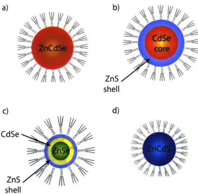
The first examples of colloidal QDs were CdSe, CdS, and CdTe nanocrystals [2]. Figure 2-5 shows the basic steps of colloidal QD synthesis. A reaction vessel containing a coordinating solvent for colloidal dispersion and electronic surface passivation is preheated to 300 C and then removed from the heat. Organometallic precursors are then are injected into the reaction vessel which results in homogeneous nucleation of nanocrystals until the reagents are depleted. This nucleation reaction causes the temperature of the vessel to drop to approximately 180 C. The reaction vessel is then gradually reheated to approximately 300 C to allow for slow growth and annealing of the QDs. The absorption spectrum of reaction solution is monitored and the growth temperature modulated to precisely control the size of the QDs. Less than 5% deviation in QD size is obtained. The QDs are precipitated and centrifuged dry to separate them from the reaction byproducts. They are then redispersed in the solvent of choice. Since this process was first developed in 1993, techniques have been developed to improve the photoluminescent efficiencies of the QDs. While CdSe and CdTe core QDs can provide tuned emission throughout the visible and infrared, there are specific techniques and material sets that work well for particular parts of the spectrum. The following paragraphs briefly describe the techniques Jonathan Halpert in the group of Professor Moungi Bawendi at MIT employed to synthesize the QDs used in this work.
Red QDs discussed here are either CdSe core QDs overcoated with ZnS ((CdSe)Zns) or ZnCdSe alloyed QDs, shown schematically in Figure 2-6a and b. (CdSe)ZnS QDs are synthesized following the method of Dabbousi et.al. [37]. The CdSe cores are made as described above. The ZnS shell is grown on the cores using a technique similar to that of the core synthesis. CdSe cores, capped in the coordinating ligands trioctylphosphine oxide (TOPO), are placed in a reaction vessel, which is heated to
1.
r"
Preheat coordinating ligands R
(-300 C)
3.
Heat solution (200-300 C) for several hours until QDs reach desired size
emove coordinating ligands from heat; inject organometallic precursors.
Nucleation reaction turns clear ligand solution yellow-green.
Trioctylphosphine oxid (TOPO) capping ligand
Figure 2-5: Schematic depicting synthesis procedure for CdSe as first described in [2].
2.
or,
b)
ZnS
///1A
shell d) CdSe d 0 ZnS / shellFigure 2-6: Schematic of the structure ZnSe/CdSe/ZnS, and d) ZnCdS QDs.
~2V~ ~
w
of a) ZnCdSe, b) (CdSe)ZnS,
a temperature between 200 and 300 C. The organometallic precursors, diethyl zinc and hexamethyldisilathiane, for the ZnS shell are slowly injected into the vessel and stirred. The solution is cooled to 90 C and left stirring for several hours. Alloyed ZnCdSe QDs are synthesized following the work of Zhong et.al. [38]. Trioctylphos-phine selenide is injected into a pot of ZnO, CdO, oleic acid, and 1-octadecene at 310 C. The QDs were precipitated twice with acetone and redispersed in chloroform.
The green QDs used in this work are "triple-decker" structures since it is dif-ficult to synthesize alloyed ZnCdSe QDs below 540 nm. "Triple decker" synthesis consists of making double shells of ZnSe and CdSe as described by Ivanov et.al. [39] and overcoating these cores with ZnS 2-6. ZnSe cores were prepared by injecting a solution of diethyl zinc, trioctylphosphine selenide (TOP-Se) and TOP into a flask of hexadecylamine (HDA) at 310 C. The cores were then grown at 270 C for 2 hours. The solution was cooled to 150 C injected into a degassed solution of TOPO and
a)
\\\
C)
hexylphosphonic acid (HPA) while a solution of dimethyl cadmium, TOP-Se and TOP was added dropwise. The solution was heated at 150 C for 19 hours. These cores, made of ZnSe and CdSe, were separated from their growth byproducts and pre-pared in a reaction vessel at 150 C. Two solutions, one of dimethyl cadmium, diethyl zinc and TOP, the other of TMS2-S and TOP were added slowly to the vessel after which the solution was cooled to room temperature. The QDs were then precipitated using methanol/butanol as above and redispersed in hexane. This process was per-formed three times, filtering after each dispersion with a 0.2m filter, and redissolving, in the final step, in chloroform. The quantum yield of the ZnSe/CdSe/ZnS QDs was measured to be approximately 65% using coumarin 540 as a standard (89% QY in ethanol).
Blue emitting QD are ZnCdS (See Figure 2-6) and are prepared by injecting a degassed solution of oleylamine and elemental sulfur into a flask under argon, which contained a clear solution of CdO and ZnO dissolved into oleic acid and octadecene at 310 C, similar to that reported by Zhong et.al. [38]. After cooling, the ZnCdS cores were then precipitated by the addition of acetone and separated from the su-pernatant by centrifugation. The QDs were then precipitated a second time using methanol/butanol, centrifuged and redispersed in chloroform. The quantum yield for the ZnCdS QDs was found to be about 48% using coumarin 480 as a dye standard (99% QY in ethanol).
Chapter 3
Design of All-Inorganic QD-LEDs
In order to first design and then make systematic improvements to a metal oxide based all-inorganic QD-LED, we characterize the electrical and structural properties of the individual layers and the interfaces of the structure. The conclusions of the work described in this chapter are perhaps best summarized in tables. Table 3.2.3 lists the growth parameters for the metal oxides that make them compatible with QDs, and Table 3.3.1 provides the approximate electronic states for the metal oxides and the QDs.
3.1
Characterization of Sputtered Films
3.1.1 Atomic Force Microscopy
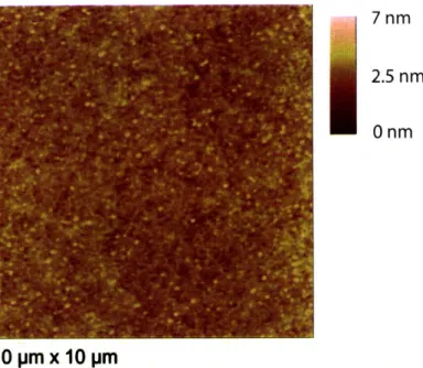
Atomic Force Microscopy (AFM) is used to study the surface quality of sputter-deposited metal oxides. In AFM, a sharp Si tip, with a radius of curvature of several nanometers and attached to the end of a cantilever, is brought in close proximity with the sample surface. The cantilever is oscillated near its resonant frequency. Forces between the sample surface and the tip alter the oscillation frequency of the cantilever. Measuring this change in the oscillation frequency provides an image of the sample surface topography.
5 nm 2.5 nm Onm
10pmx10pm 5pmx5pm
Figure 3-1: Atomic Force Microscopy surface topography images of a) ITO RF-sputtered on glass, and b) NiO RF-RF-sputtered onto the ITO shown in (a)
roughness of the NiO deposited on top of the ITO, causing current shunts through the device structure and device yields of only about 50%. One of the first steps to designing efficient devices with large yields is therefore to develop consistent proce-dures for sputter depositing smooth metal oxide layers. Sputtering a series of films with different growth conditions and characterizing their surfaces with AFM revealed that depositing ITO on glass at a rate of 0.06 A/s using a power of 12 W in an inert Ar atmosphere at 4 mTorr achieves a surface roughness of less than 1 nm rms (Figure 3-1a). Heating of the substrate during growth was required to control the ITO resistivity. NiO sputtered onto this ITO at a deposition rate of 0.2 A/s in a 1:100 02 to Ar atmosphere at 6 mTorr using 210 W of RF power maintains the film
smoothness (Figure 3-1b).
Co-sputtered ZnO and SnO2 (ZnO: SnO2) can also be used as a hole transport
layer (See Section 4.4). Figure 3-2 shows a ZnO: Sn02 on ITO surface with only
0.56 nm rms roughness. The ZnO: SnO2 was deposited by simultaneous sputtering
ZnO at 15 W and SnO2 at 9 W RF power in an argon environment at 4mTorr. This
corresponds to a 0.2 A/s deposition rate. These deposition powers were selected to tune the conductivity of the film; as long as the power for each deposition remains under 20 W, the film surface is smooth.
b.
7 nm
2.5 nm
O nm
10 pm x 10 pm
Figure 3-2: Atomic Force Microscopy surface topography images showing smooth ZnO: SnO2 on top of the ITO in Figure 3-1a
3.1.2
X-Ray Diffraction
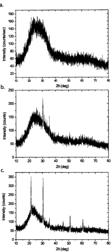
X-Ray Power Diffraction (XRPD) can be used to analyze the crystalline structure of materials. X-rays incident on a crystal with lattice planes spaced a distance d
apart are reflected off the crystal ions. The path difference between reflections from neighboring lattice planes is equal to 2dsin(6). If this path difference is equal to an integer number of wavelengths, constructive interference will result. This is commonly referred to as Bragg's condition. If the material is crystalline (has good periodicity), at certain values of 6, all the reflections will be in phase and result in discrete, sharp peaks in a collected intensity vs. 9 plot. In amorphous solids, which lack a periodic structure, these peaks are not present. [28]
The ceramic materials used in our devices (See Table 3.2.3 for information on deposition parameters) were measured using a Rigaku Powder Diffractometer, which consists of a high-powered rotating anode generator that supplies X-rays to a 250mm Bragg-Brentano diffractometer. Figure 3-3 shows the X-ray diffraction spectra for the different types of ITO used in our structure. Often the top electrode of our devices is ITO deposited as described in Section 3.1.1 but without heat, which would
damage the QD layer. Figure 3-3a shows this RF sputtered ITO to be amorphous. When ITO is deposited under the same conditions and with heat, estimated to be about 250 C at the substrate surface, the film becomes polycrystalline (Figure 3-3b). Commercially purchased ITO exhibits even more crystalline features (Figure 3-3c). Either the commercially purchased ITO or the ITO sputtered in a heated chamber can be used as the bottom electrode.
Figure 3-4 shows the X-ray diffraction spectra for the charge transport layers. Figure 3-4a indicates that the NiO we grow is in its natural occurring from, bun-senite, which has a cubic structure that exhibits predominately (111) faces with an octahedral morphology. The ZnS film appears completely amorphous. The ZnO is polycrystalline. Crystalline wurtzite ZnO has unit cell dimensions a = 3.250A and c = 5.207A. S1n 2 is a tetragonal rutile structure with unit cell dimensions of a 4.737A and c = 3.186A [40]. As expected for a film that is blend of two materials with different crystal structures and sizes, ZnO : SnO2 is amorphous.
This XRPD data highlights several aspects of all inorganic QD-LED design that are not yet fully understood. First, the devices with any of the three types of ITO electrodes turn on, indicating that a smooth surface - not the crystal morphology of the film - is the critical parameter. However, it is unclear whether different degrees of crystallinity lead to non-uniformities in lateral conductivity that may effect device yields, performance, and stability. Furthermore, we do not know whether the degree of ordering in the ITO layer alters the subsequent material deposition. Secondly, we aim to deposit amorphous charge transport layers, reasoning that defects or grain boundaries in a polycrystalline material could result in unwanted current pathways and a shunted device. While ZnS and ZnO : Sn0 2 are amorphous, ZnO and NiO show some crystal structure. Further experiments will be done to determine whether more crystalline films improve the device performance. For example, crystalline ZnO is a wurzite structure, which does not possess an inversion center, so polar or nonpolar surface states can develop depending on which index face is exposed [40]. Control over the ZnO surface could perhaps be used to facilitate deposition and stability of QDs next to ZnO.
![Figure 1-1: Schematic of liquid crystal cell [1].](https://thumb-eu.123doks.com/thumbv2/123doknet/13928563.450447/16.918.195.729.147.529/figure-schematic-liquid-crystal-cell.webp)
![Figure 1-3: a) Normalized electroluminescence spectra for QDs showing their narrow band emission throughout in the visible and infrared region of the spectra [3], [4]](https://thumb-eu.123doks.com/thumbv2/123doknet/13928563.450447/19.918.154.783.142.518/figure-normalized-electroluminescence-spectra-showing-emission-visible-infrared.webp)

![Figure 2-5: Schematic depicting synthesis procedure for CdSe as first described in [2].](https://thumb-eu.123doks.com/thumbv2/123doknet/13928563.450447/39.918.189.746.241.913/figure-schematic-depicting-synthesis-procedure-cdse-described.webp)